2021 \unnumbered
[1]\fnmTom \surDvir \equalcontThese authors contributed equally to this work.
These authors contributed equally to this work.
These authors contributed equally to this work.
1]\orgdivQuTech and Kavli Institute of NanoScience, \orgnameDelft University of Technology, \postcode2600 GA \orgaddress\cityDelft, \countryThe Netherlands
2]\orgdivDepartment of Applied Physics, \orgnameEindhoven University of Technology, \postcode5600 MB \orgaddress\cityEindhoven, \countryThe Netherlands
Realization of a minimal Kitaev chain in coupled quantum dots
Abstract
Majorana bound states constitute one of the simplest examples of emergent non-Abelian excitations in condensed matter physics. A toy model proposed by Kitaev shows that such states can arise at the ends of a spinless -wave superconducting chain Kitaev.2001 . Practical proposals for its realization Sau.2012 ; Leijnse.2012 require coupling neighboring quantum dots in a chain via both electron tunneling and crossed Andreev reflection Recher.2001 . While both processes have been observed in semiconducting nanowires and carbon nanotubes hofstetter2009cooper ; herrmann2010carbon ; das2012high-efficiency ; schindele2012near-unity , crossed-Andreev interaction was neither easily tunable nor strong enough to induce coherent hybridization of dot states. Here we demonstrate the simultaneous presence of all necessary ingredients for an artificial Kitaev chain: two spin-polarized quantum dots in an InSb nanowire strongly coupled by both elastic co-tunneling and crossed Andreev reflection. We fine-tune this system to a sweet spot where a pair of Poor Man’s Majorana states is predicted to appear. At this sweet spot, the transport characteristics satisfy the theoretical predictions for such a system, including pairwise correlation, zero charge and stability against local perturbations. While the simple system presented here can be scaled to simulate a full Kitaev chain with an emergent topological order, it can also be used imminently to explore relevant physics related to non-Abelian anyons.
Engineering Majorana bound states in condensed matter systems is an intensively pursued goal, both for their exotic non-Abelian exchange statistics and for potential applications in building topologically protected qubits Kitaev.2001 ; Nayak.2008 ; Kitaev.2003 . The most investigated experimental approach looks for Majorana states at the boundaries of topological superconducting materials, made of hybrid semiconducting-superconducting heterostructures Mourik.2012 ; Deng2016 ; Fornieri2019 ; ren2019topological ; Vaitieknas2020 . However, the widely-relied-upon signature of Majorana states, zero-bias conductance peaks, is by itself unable to distinguish topological Majorana states from other trivial zero-energy states induced by disorder and smooth gate potentials Kells2012 ; Prada2012 ; Pikulin2012 ; Liu2017andreev ; Vuik.2019 ; Pan.2020.Physical . Both problems disrupting the formation or detection of a topological phase originate from a lack of control over the microscopic details of the electron potential landscape in these heterostructure devices.
In this work, we realize a minimal Kitaev chain Kitaev.2001 using two quantum dots (QDs) coupled via a short superconducting-semiconducting hybrid Sau.2012 . By controlling the electrostatic potential on each of these three elements, we overcome the challenge imposed by random disorder potentials. At a fine-tuned sweet spot where Majorana states are predicted to appear, we observe end-to-end correlated conductance that signals emergent Majorana properties such as zero charge and robustness against local perturbations. We note that these Majorana states in a minimal Kitaev chain are not topologically protected and have been dubbed “Poor Man’s Majorana” (PMM) states Leijnse.2012 .
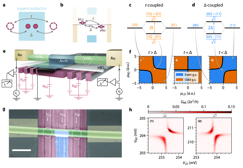
The elementary building block of the Kitaev chain is a pair of spinless electronic sites coupled simultaneously by two mechanisms: elastic co-tunneling (ECT) and crossed Andreev reflection (CAR). Both processes are depicted in Fig. 1a. ECT involves a single electron hopping between two sites with an amplitude . CAR refers to two electrons from both sites tunneling back and forth into a common superconductor with an amplitude (not to be confused with the superconducting gap size), forming and splitting Cooper-pairs Recher.2001 . To create the two-site Kitaev chain, we utilize two spin-polarized QDs where only one orbital level in each dot is available for transport. In the absence of tunneling between the QDs, the system is characterized by a well-defined charge state on each QD: , where are occupations of the left and right QD levels. The charge on each QD depends only on its electrochemical potential or , schematically shown in Fig. 1b.
In the presence of inter-dot coupling, the eigenstates of the combined system become superpositions of the charge states. ECT couples and , resulting in two eigenstates of the form (Fig. 1c), both with odd combined charge parity. These two bonding and anti-bonding states differ in energy by when both QDs are at their charge degeneracy, i.e., . Analogously, CAR couples the two even states and to produce bonding and anti-bonding eigenstates of the form , preserving the even parity of the original states. These states differ in energy by when (Fig. 1d). If the amplitude of ECT is stronger than CAR (), the odd bonding state has lower energy than the even bonding state near the joint charge degeneracy (see Methods for details). The system thus features an odd ground state in a wider range of QD potentials, leading to a charge stability diagram shown in Fig. 1f(i) Wiel.2003erp . The opposite case of CAR dominating over ECT, i.e., , leads to a charge stability diagram shown in Fig. 1f(iii), where the even ground state is more prominent. Fine-tuning the system such that equalizes the two avoided crossings, inducing an even-odd degenerate ground state at (Fig. 1f(ii)). This degeneracy gives rise to two spatially separated PMMs, each localized at one QD Leijnse.2012 .
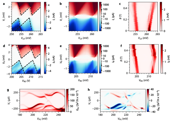
Fig. 1e illustrates our coupled QD system and the electronic measurement circuit. An InSb nanowire is contacted on two sides by two Cr/Au normal leads (N). A -wide superconducting lead (S) made of a thin Al/Pt film covering the nanowire is grounded and proximitizes the central semiconducting segment. The chemical potential of the proximitized semiconductor can be tuned by gate voltage . This hybrid segment shows a hard superconducting gap accompanied by discrete, gate-tunable Andreev bound states (Fig. ED1). Two QDs are defined by finger gates underneath the nanowire. Their chemical potentials are linearly tuned by voltages on the corresponding gates . Bias voltages on the two N leads, , are applied independently and currents through them, , are measured separately. Transport characterization shows charging energies of on the left QD and on the right (Fig. ED1). Standard DC+AC lock-in technique allows measurement of the full conductance matrix:
| (1) |
Measurements were conducted in a dilution refrigerator in the presence of a magnetic field applied approximately along the nanowire axis. The combination of Zeeman splitting and orbital level spacing allows single-electron QD transitions to be spin-polarized. Two neighbouring Coulomb resonances correspond to opposite spin orientations, enabling the QD spins to be either parallel ( and ) or anti-parallel ( and ). We report on two devices, A in the main text and B in Extended Data (Fig. ED7 and Fig. ED8). A scanning electron microscope image of Device A is shown in Fig. 1g.
Transport measurements are used to characterize the charge stability diagram of the system. In Fig. 1h(1), we show as a function of QD voltages when both QDs are set to spin-down (). The measured charge stability diagram shows avoided crossing which indicates the dominance of ECT. In Fig. 1h(2), we change the spin configuration to . The charge stability diagram now develops the avoided crossing of the opposite orientation, indicating the dominance of CAR for QDs with anti-parallel spins. This is, to our knowledge, the first verification of the prediction that spatially separated QDs can coherently hybridize via CAR coupling to a superconductor choi2000spin . Thus, we have introduced all the necessary ingredients for a two-site Kitaev chain.
1 Tuning the relative strength of CAR and ECT
Majorana states in long Kitaev chains are present under a wide range of parameters due to topological protection Kitaev.2001 . Strikingly, even a chain consisting of only two sites can host a pair of PMMs despite a lack of topological protection, if the fine-tuned sweet spot and can be achieved Leijnse.2012 . This, however, is made challenging by the above-mentioned requirement to have both QDs spin-polarized. If spin is conserved, ECT can only take place between QDs with or spins, while CAR is only allowed for and . Rashba spin-orbit coupling in InSb nanowires solves this dilemma Sau.2012 ; Liu.2022 ; wang2022Singlet , allowing finite ECT even in anti-parallel spin configurations and CAR between QDs with equal spins.
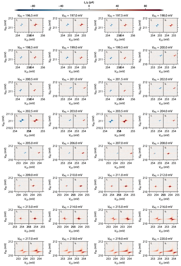
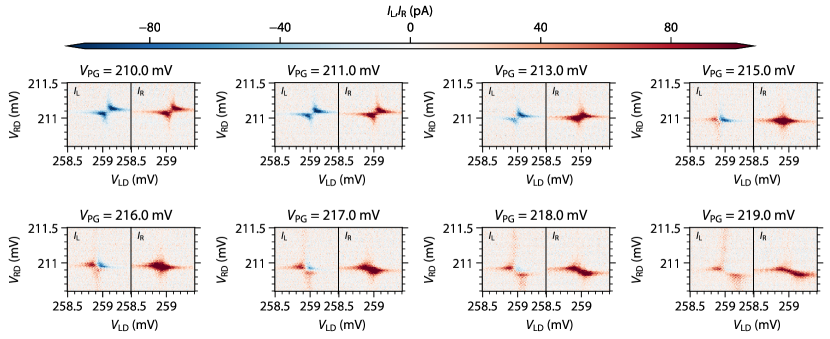
A further challenge is to make the two coupling strengths equal for a given spin combination. Refs. Liu.2022 ; wang2022Singlet ; bordin2022controlled show that both CAR and ECT in our device are virtual transitions through intermediate Andreev bound states residing in the short InSb segment underneath the superconducting film. Thus, varying changes the energy and wavefunction of said Andreev bound states and thereby . We search for the range over which changes differently than and look for a crossover in the type of charge stability diagrams.
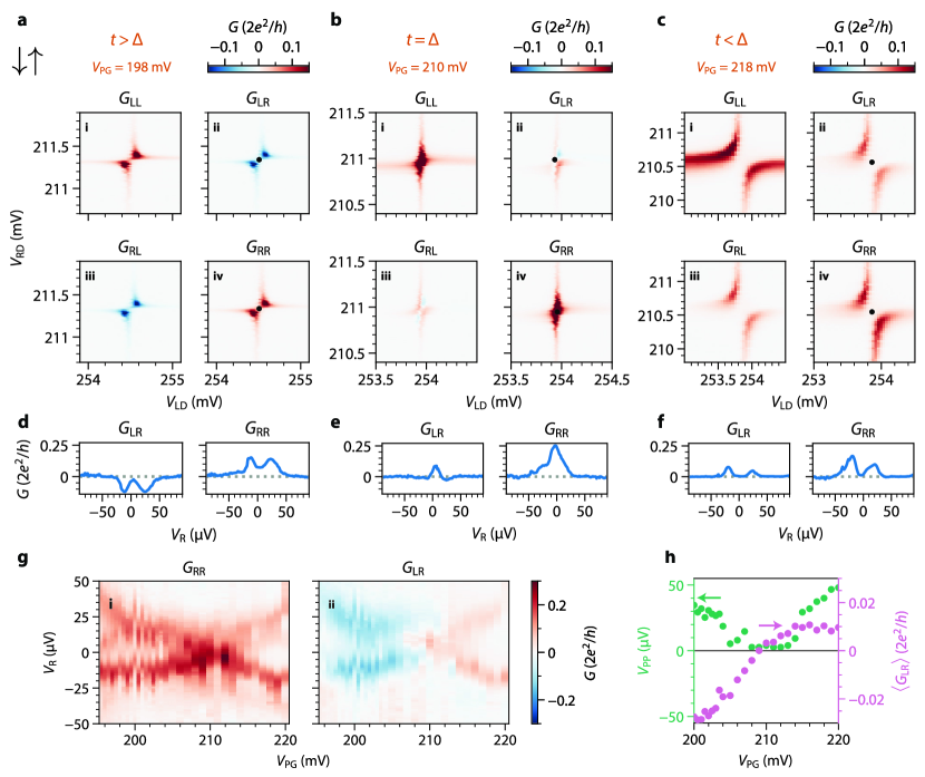
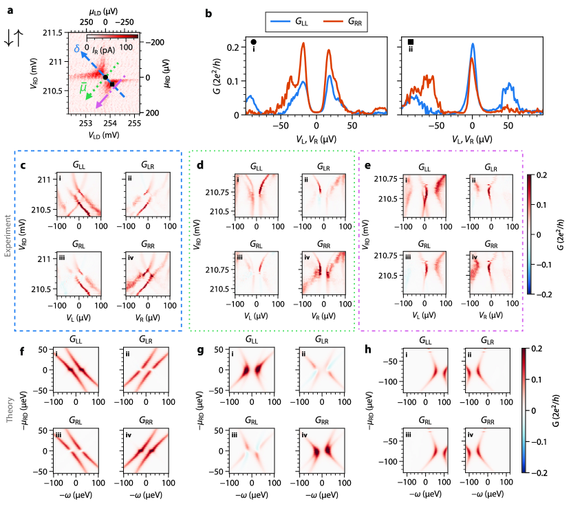
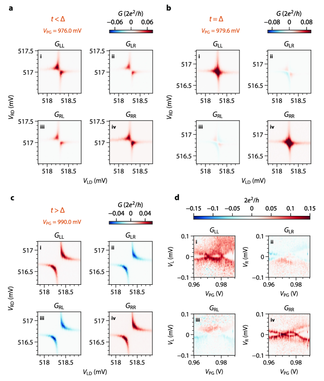
Fig. 2a-c shows the resulting charge stability diagrams for the spin configuration at different values of . The conductance matrix at is shown in Fig. 2a. The local conductance on both sides, and , exhibit level repulsion indicative of . We emphasize that ECT can become stronger than CAR even though the spins of the two QD transitions are anti-parallel due to the electric gating mentioned above. The dominance of ECT over CAR can also be seen in the negative sign of the nonlocal conductance, and . During ECT, an electron enters the system through one dot and exits through the other, resulting in negative nonlocal conductance. CAR, in contrast, causes two electrons to enter or leave both dots simultaneously, producing positive nonlocal conductance Beckmann2006 . The residual finite conductance in the center of the charge stability diagram can be attributed to level broadening due to finite temperature and dot-lead coupling (see Fig. ED10). In Fig. 2d, we show the conductance spectrum measured as a function of , with and tuned to (black dots in panels c(ii, iv)). A pair of conductance peaks or dips is visible on either side of zero energy.
Fig. 2c shows at (the component is also used for Fig. 1h(2)). Here, all the elements of exhibit CAR-type avoided crossings. The spectrum shown in panel f, obtained at the joint charge degeneracy point (black dots in panels c(ii, iv)), similarly has two conductance peaks surrounding zero energy. The measured nonlocal conductance is positive as predicted for CAR. The existence of both and regimes, together with continuous gate tunability, allows us to approach the sweet spot. This is shown in panel b, taken with . Here, and exhibit no avoided crossing while and fluctuate around zero, confirming that CAR and ECT are in balance. Accordingly, the spectrum in panel e confirms the even and odd ground states are degenerate and transport can occur at zero excitation energy via the appearance of a zero-bias conductance peak. The crossover from the regime to the regime can be seen across multiple QD resonances (Fig. ED9).
To show that gate-tuning of the ratio is indeed continuous, we repeat charge stability diagram measurements (Fig. ED3) and bias spectroscopy at more values. As before, each bias sweep is conducted while keeping both QDs at charge degeneracy. Fig. 2g shows the resulting composite plot of (i) and (ii) vs bias voltage and . The X-shaped conductance feature indicates a continuous evolution of the excitation energy, with a linear zero-energy crossing agreeing with predictions in Ref. Leijnse.2012 . Following analysis described in Methods, we extract the peak spacing and average nonlocal conductance in Fig. 2h in order to visualize the continuous crossover from to .
2 Poor Man’s Majorana sweet spot
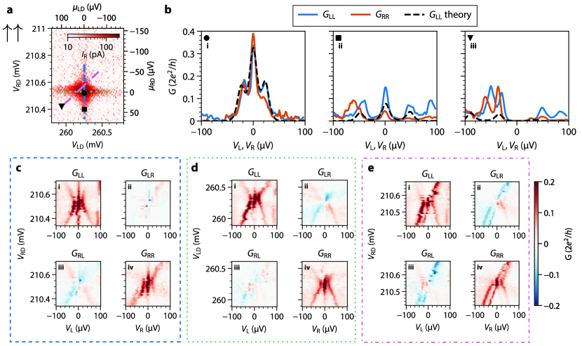
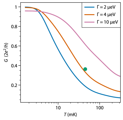
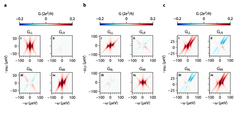
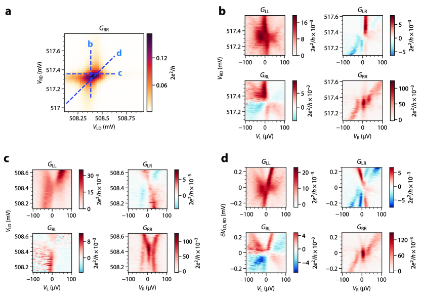
Next, we study the excitation spectrum in the vicinity of the sweet spot. The predicted zero-temperature experimental signature of the PMMs is a pair of quantized zero-bias conductance peak on both sides of the devices. These zero-bias peaks are persistent even when one of the QD levels deviates from charge degeneracy Leijnse.2012 . We focus on the spin configuration since it exhibits higher values when they are equal (see Fig. ED4). Fig. 3a shows the charge stability diagram measured via under fixed . No level repulsion is visible, indicating . Panel b(i) shows the excitation spectrum when both dots are at charge degeneracy. The spectra on both sides show zero-bias peaks accompanied by two side peaks. The values of can be read directly from the position of the side peaks, which correspond to the anti-bonding excited states at energy . The height of the observed zero-bias peaks is 0.3 to , likely owing to a combination of tunnel broadening and finite electron temperature (Fig. ED2). Fig. 3b(ii) shows the spectrum when the right QD is moved away from charge degeneracy while is kept at 0. The zero-bias peaks persist on both sides of the device, as expected for a PMM state. In contrast, tuning both dots away from charge degeneracy, shown in Fig. 3b(iii), splits the zero-bias peaks.
In Fig. 3c,d, we show the evolution of the spectrum when varying and , respectively. The vertical feature appearing in both and shows correlated zero-bias peaks in both QDs, which persist when one QD potential departs from zero. This crucial observation demonstrates the robustness of PMMs against local perturbations. The excited states disperse in agreement with the theoretical predictions Leijnse.2012 . Nonlocal conductance, on the other hand, reflects the local charge character of a bound state on the side where current is measured gramich2017andreev ; Danon.2020 ; Menard.2020 . Near-zero values of in panel c and in panel d are consistent with the prediction that the PMM mode on the unperturbed side remains an equal superposition of an electron and a hole and therefore chargeless.
Finally, when varying the chemical potential of both dots simultaneously (panel e), we see that the zero-bias peaks split away from zero energy. This splitting is not linear, in contrast to the case when (see Fig. ED5). The profile of the peak splitting is consistent with the predicted quadratic protection of PMMs against chemical potential fluctuations Leijnse.2012 . This quadratic protection is expected to develop into topological protection in a long-enough Kitaev chain Sau.2012 .
3 Discussion
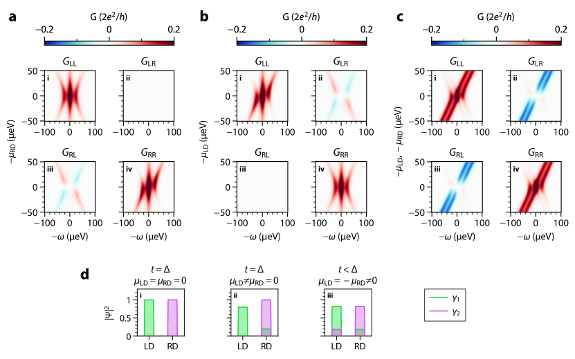
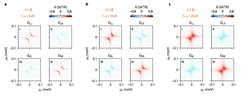
To facilitate comparison with data, we develop a transport model (see Methods) and plot in Fig. 4a-c the calculated conductance matrices as functions of excitation energy, , vs (panel a), (panel b), and (panel c). These conditions are an idealization of those in Fig. 3 (a more realistic simulation of the experimental conditions is presented in Fig. ED6). The numerical simulations capture the main features appearing in the experiments discussed above.
Particle-hole symmetry ensures that zero-energy excitations in this system always come in pairs. These excitations can extend over both QDs or be confined to one of them. In Fig. 4d we show the calculated spatial extent of the zero-energy excitations for three scenarios. The first, in Fig. 4d(i), illustrates Fig. 3b(i) and shows that the sweet-spot zero-energy solutions are two PMMs, each localized on a different QD. The second scenario in Fig. 4d(ii), illustrating Fig. 3b(ii), is varying while keeping . This causes some of the wavefunction localized on the perturbed left side, , to leak into the right QD. Since the right-side excitation has no weight on the left, it does not respond to this perturbation and remains fully localized on the right QD. As the theory confirms Leijnse.2012 , it stays a zero-energy PMM state. Since Majorana excitations always come in pairs, the excitation on the left QD must also remain at zero energy. This provides an intuitive understanding of the remarkable stability of the zero-energy modes at the sweet spot in Fig. 3c,d when moving one of the QDs’ chemical potentials away from zero. Finally, zero-energy solutions can be found away from the sweet spot, , as illustrated in Fig. 4d(iii). These zero-energy states are only found when both QDs are off-resonance and none of them are localized Majorana states, extending over both QDs and exhibiting no gate stability. Measurements under these conditions are shown in Fig. ED5, where zero-energy states can be found in a variety of gate settings (panels a, c therein).
4 Conclusion
In summary, we realize a minimal Kitaev chain where two QDs in an InSb nanowire are separated by a hybrid semiconducting-superconducting segment. Compared to past works, our approach solves three challenges: strong hybridization of QDs via CAR, simultaneous coupling of two single spins via both ECT and CAR, and continuous tuning of the coupling amplitudes. This is made possible by the two QDs as well as the middle Andreev bound state mediating their couplings all being discrete, gate-tunable quantum states. The result is the creation of a new type of nonlocal states that host Majorana-type excitations at a fine-tuned sweet spot. The zero-bias peaks at this spot are robust against variations of the chemical potential of one QD and quadratically protected against simultaneous perturbations of both. This discrete and tunable way of assembling Kitaev chains shows good agreement between theory and experiment by avoiding the most concerning problems affecting the continuous nanowire experiments: disorder, smooth gate potentials and multi-subband occupation Pan.2021.KitaevVsNanowire . The QD-S-QD platform discussed here opens up a new frontier to the study of Majorana physics. In the long term, this approach can generate topologically protected Majorana states in longer chains Sau.2012 . A shorter term approach is to use PMMs as an immediate playground to study fundamental non-Abelian statistics, e.g., by fusing neighboring PMMs in a device with two such copies.
5 Methods
5.1 Device fabrication
The nanowire hybrid devices presented in this work were fabricated on pre-patterned substrates, using the shadow-wall lithography technique described in Refs. Heedt:2021_NC ; Borsoi:2021_AFM . Nanowires were deposited onto the substrates using an optical micro-manipulator setup. of Al was grown at a mix of 15∘ and 45∘ angles with respect to the substrate. Subsequently, Device A was coated with of Pt grown at 30∘. No Pt was deposited for Device B. Finally, all devices were capped with of evaporated AlOx. Details of the substrate fabrication, the surface treatment of the nanowires, the growth conditions of the superconductor, the thickness calibration of the Pt coating and the ex-situ fabrication of the ohmic contacts can be found in Ref. Mazur.2022 . Devices A and B also slightly differ in the length of the hybrid segment: for A and for B.
5.2 Transport measurement and data processing
We have fabricated and measured six devices with similar geometry. Two of them showed strong hybridization of the QD states by means of CAR and ECT. We report on the detailed measurements of Device A in the main text and show qualitatively similar measurements from Device B in Fig. ED7 and Fig. ED8. All measurements on Device A were done in a dilution refrigerator with base temperature at the cold plate and electron temperature of 40 at the sample, measured in a similiar setup using an NIS metallic tunnel junction. Unless otherwise mentioned, the measurements on Device A were conducted in the presence of a magnetic field of approximately oriented along the nanowire axis with a 3∘ offset. Device B was measured similarly in another dilution refrigerator under along the nanowire with 4∘ offset.
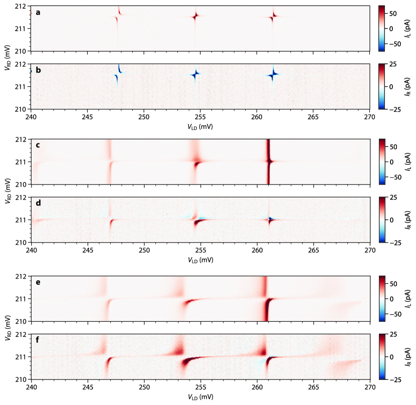
Fig. 1e shows a schematic depiction of the electrical setup used to measure the devices. The middle segment of the InSb nanowire is covered by a thin Al shell, kept grounded throughout the experiment. On each side of the hybrid segment, we connect the normal leads to a current-to-voltage converter. The amplifiers on the left and right sides of the device are each biased through a digital-to-analog converter that applies DC and AC biases. The total series resistance of the voltage source and the current meter is less than for Device A and for Device B. Voltage outputs of the current meter are read by digital multimeters and lock-in amplifiers. When DC voltage is applied, is kept grounded and vice versa. AC excitations are applied on each side of the device with different frequencies ( on the left and on the right for Device A, on the left and on the right for Device B) and with amplitudes between 2 and RMS. In this manner, we measure the DC currents and the conductance matrix in response to applied voltages on the left and right N leads, respectively. The conductance matrix is corrected for voltage divider effects (see Ref. Martinez2021 for details) taking into account the series resistance of sources and meters and in each fridge line ( for Device A and for Device B), except for the right panel of Fig. 1h and Fig. 2d. There, the left half of the conductance matrix was not measured and correction is not possible. We verify that the series resistance is much smaller than device resistance and the voltage divider effect is never more than of the signal.
5.3 Characterization of QDs and the hybrid segment
To form the QDs described in the main text, we pinch off the finger gates next to the three ohmic leads, forming two tunnel barriers in each N-S junction. and applied on the middle finger gates on each side accumulate electrons in the QDs. We refer to the associated data repository for the raw gate voltage values used in each measurement. See Fig. ED1a-f for results of the dot characterizations.
Characterization of the spectrum in the hybrid segment is done using conventional tunnel spectroscopy. In each uncovered InSb segment, we open up the two finger gates next to the N lead and only lower the gate next to the hybrid to define a tunnel barrier. The results of the tunnel spectroscopy are shown in Fig. ED1g,h and the raw gate voltages are available in the data repository.
5.4 Determination of QD spin polarization
Control of the spin orientation of QD levels is done via selecting from the even vs odd charge degeneracy points following the method detailed in Ref. Hanson.2007 . At the charge transition between occupancy and ( being an integer), the electron added to or removed from the QD is polarized to spin-down (, lower in energy). The next level available for occupation, at the transition between and electrons, has the opposite polarization of spin-up (, higher in energy). To ensure the spin polarization is complete, the experiment was conducted with (see Fig. ED1 for determination of the spin configuration). In the experiment data, a change in the QD spin orientation is visible as a change in the range of or .
5.5 Controlling ECT and CAR via electric gating
Ref. Liu.2022 describes a theory of mediating CAR and ECT transitions between QDs via virtual hopping through an intermediate Andreev bound state. Ref. bordin2022controlled experimentally verifies the applicability of this theory to our device. To summarize the findings here, we consider two QDs both tunnel-coupled to a central Andreev bound state in the hybrid segment of the device. The QDs have excitation energies lower than that of the Andreev bound state and thus transition between them is second-order. The wavefunction of an Andreev bound state consists of a superposition of an electron part, , and a hole part, . Both theory and experiment conclude that the values of and depend strongly and differently on . Specifically, CAR involves converting an incoming electron to an outgoing hole and thus depends on the values of and jointly as . ECT, however, occurs over two parallel channels (electron-to-electron and hole-to-hole) and its coupling strength depends on independently as . As the composition of is a function of the chemical potential of the middle Andreev bound state, the CAR to ECT ratio is strongly tunable by . We thus look for a range of where Andreev bound states reside in the hybrid segment, making sure that the energies of these states are high enough so as not to hybridize with the QDs directly (Fig. ED1). Next, we sweep to find the crossover point between and as described in the main text.
5.6 Additional details on the measurement of the coupled QD spectrum
The measurement of the local and nonlocal conductance shown in Fig. 2g was conducted in a series of steps. First, the value of was set, and a charge stability diagram was measured as a function of and . Representative examples of such diagrams are shown in Fig. ED3. Second, each charge stability diagram was inspected and the joint charge degeneracy point () was selected manually (). Lastly, the values of and were set to those of the joint degeneracy point and the local and nonlocal conductance were measured as a function of .
The continuous transition from to is visible in Fig. 2g via both local and nonlocal conductance. shows that level repulsion splits the zero-energy resonance peaks both when (lower values of ) and when (higher values of ). The zero-bias peak is restored in the vicinity of , in agreement with theoretical predictions Leijnse.2012 . The crossover is also apparent in the sign of , which changes from negative () to positive ().
To better visualize the transition between the ECT- and CAR-dominated regimes, we extract , the separation between the conductance peaks under positive and negative bias voltages, and plot them as a function of in Fig. 2h. When tuning , the peak spacing decreases until the two peaks merge at . Further increase of leads to increasing . In addition, to observe the change in sign of the nonlocal conductance, we follow , the value of averaged over the bias voltage between and at a given . We see that turns from negative to positive at , in correspondence to a change in the dominant coupling mechanism.
Fig. 3c-e presents measurements where the conductance was measured against applied biases along some paths within the charge stability diagram (panel a). Prior to each of these measurements, a charge stability diagram was measured and inspected, based on which the relevant path in the plane was chosen. Following each bias spectroscopy measurement, another charge stability diagram was measured and compared to the one taken before to check for potential gate instability. In case of noticeable gate drifts between the two, the measurement was discarded and the process was repeated. The values of and required for theoretical curves appearing in panel b were calculated by where and is the lever arm of the corresponding QD. The discrepancy between the spectra measured with and likely results from gate instability, since they were not measured simultaneously. Finite remaining in panel c and in panel d most likely result from small deviations of from zero during these measurements.
5.7 Model of the phase diagrams in Fig. 1f
To calculate the ground state phase diagram in Fig. 1f, we write the Hamiltonian in the many-body picture, with the four basis states being :
| (2) |
in block-diagonalized form. The two matrices yield the energy eigenvalues separately for the even and odd subspaces:
| (3) | ||||
| (4) |
The ground state phase transition occurs at the boundary . This is equivalent to
| (5) |
5.8 Transport model in Fig. 3 and Fig. 4
We describe in this section the model Hamiltonian of the minimal Kitaev chain and the method we use for calculating the differential conductance matrices when the Kitaev chain is tunnel-coupled to two external N leads.
The effective Bogoliubov-de-Gennes Hamiltonian of the double-QD system is
| (6) |
where is the Nambu spinor, is the level energy in dot- relative to the superconducting Fermi surface, and are the ECT and CAR amplitudes. Here we assume and to be real without loss of generality Leijnse.2012 . The presence of both and in this Hamiltonian implies breaking spin conservation during QD-QD tunneling via either spin-orbit coupling (as done in the present experiment) or non-collinear magnetization between the two QDs (as proposed in Leijnse.2012 ). Without one of them, equal-spin QDs cannot recombine into a Cooper pair, leading to vanishing , while opposite-spin QDs cannot support finite . The exact values of and depend on the spin-orbit coupling strength and we refer to Ref. Liu.2022 for a detailed discussion.
To calculate the differential conductance for the double-QD system, we use the -matrix method datta2005quantum . In the wide-band limit, the matrix is
| (7) |
where is the tunnel matrix, with being the tunnel coupling strength between dot- and lead-. The zero-temperature differential conductance is given by
| (8) |
where . Finite-temperature effect is included by a convolution between the zero-temperature conductance and the derivative of Fermi-Dirac distribution, i.e.,
| (9) |
The theoretical model presented above uses five input parameters to calculate the conductance matrix under given . The input parameters are: . To choose the parameters in Fig. 3b(i), we fix the temperature to the measured value and make the simplification , . This results in only two free parameters , which we manually choose and compare with data. While oversimplified, this approach allows us to obtain a reasonable match between theory and data taken at without the risk of overfitting. To obtain the other numerical curves shown in Fig. 3, we keep the same choice of and vary along various paths in the parameter space. Similarly, to model the data shown in Fig. ED5, we keep and the same as in Fig. 3. The free parameters to be chosen are thus and . The theory panels are obtained with the same , and only are varied in accordance with the experimental conditions.
Finally, we comment on the physical meaning of the theory predictions in Fig. 4a-c. Tuning leads to symmetric and asymmetric , as well as zero and finite with an alternating pattern of positive and negative values. As discussed in the main text, these features, also seen in the measurements, stem from the local charge of the system: keeping maintains zero local charge on the left dot, while varying creates finite local charge on the right dot. The complementary picture appears when varying in panel b. The asymmetry in both and and the negative nonlocal conductance when tuning simultaneously are also captured in the numerical simulation in panel c. We note that while there is a qualitative agreement between the features in Fig. 4c and Fig. 3e, they were obtained under nominally different conditions. As mentioned, the theoretical curve follows , while the experimental curve was taken through a path along which changed twice as much as , although the lever arms of both QDs are similar. In Fig. 4c, we calculate the conductance along a path reproducing the experimental conditions. We speculate that the discrepancy between Fig. 3e and Fig. 4c could arise from some hybridization between the left QD and the superconducting segment as seen in Fig. ED1.
5.9 Data Availability and Code Availability
Raw data presented in this work, the data processing/plotting code and code used for the theory calculations are available at https://doi.org/10.5281/zenodo.6594169.
6 Extended data
References
- \bibcommenthead
- (1) Kitaev, A.Y.: Unpaired Majorana fermions in quantum wires. Physics-Uspekhi 44(10S), 131 (2001) cond-mat/0010440. https://doi.org/10.1070/1063-7869/44/10s/s29
- (2) Sau, J.D., Sarma, S.D.: Realizing a robust practical Majorana chain in a quantum-dot-superconductor linear array. Nature Communications 3(1), 964 (2012) 1111.6600. https://doi.org/10.1038/ncomms1966
- (3) Leijnse, M., Flensberg, K.: Parity qubits and poor man’s Majorana bound states in double quantum dots. Physical Review B 86(13), 134528 (2012) 1207.4299. https://doi.org/10.1103/physrevb.86.134528
- (4) Recher, P., Sukhorukov, E.V., Loss, D.: Andreev tunneling, Coulomb blockade, and resonant transport of nonlocal spin-entangled electrons. Physical Review B 63(16), 165314 (2001) cond-mat/0009452. https://doi.org/10.1103/physrevb.63.165314
- (5) Hofstetter, L., Csonka, S., Nygård, J., Schönenberger, C: Cooper pair splitter realized in a two-quantum-dot Y-junction 461. https://doi.org/10.1038/nature08432
- (6) Herrmann, L.G., Portier, F., Roche, P., Yeyati, A.L., Kontos, T., Strunk, C.: Carbon nanotubes as Cooper-pair beam splitters 104(2), 026801. https://doi.org/10.1103/PhysRevLett.104.026801. Publisher: American Physical Society
- (7) Das, A., Ronen, Y., Heiblum, M., Mahalu, D., Kretinin, A.V., Shtrikman, H.: High-efficiency Cooper pair splitting demonstrated by two-particle conductance resonance and positive noise cross-correlation 3, 1165–1166. https://doi.org/10.1038/ncomms2169. Publisher: Nature Publishing Group
- (8) Schindele, J., Baumgartner, A., Schönenberger, C.: Near-unity Cooper pair splitting efficiency 109(15), 157002. https://doi.org/10.1103/PhysRevLett.109.157002
- (9) Nayak, C., Simon, S.H., Stern, A., Freedman, M., Sarma, S.D.: Non-Abelian anyons and topological quantum computation. Reviews of Modern Physics 80(3), 1083–1159 (2008) 0707.1889. https://doi.org/10.1103/revmodphys.80.1083
- (10) Kitaev, A.Y.: Fault-tolerant quantum computation by anyons. Annals of Physics 303(1), 2–30 (2003) quant-ph/9707021. https://doi.org/10.1016/s0003-4916(02)00018-0
- (11) Mourik, V., Zuo, K., Frolov, S.M., Plissard, S.R., Bakkers, E.P.A.M., Kouwenhoven, L.P.: Signatures of Majorana fermions in hybrid superconductor-semiconductor nanowire devices. Science 336(6084), 1003–1007 (2012) 1204.2792. https://doi.org/10.1126/science.1222360
- (12) Deng, M.T., Vaitiekėnas, S., Hansen, E.B., Danon, J., Leijnse, M., Flensberg, K., Nygård, J., Krogstrup, P., Marcus, C.M.: Majorana bound state in a coupled quantum-dot hybrid-nanowire system. Science 354(6319), 1557–1562 (2016). https://doi.org/10.1126/science.aaf3961
- (13) Fornieri, A., Whiticar, A.M., Setiawan, F., Portolés, E., Drachmann, A.C.C., Keselman, A., Gronin, S., Thomas, C., Wang, T., Kallaher, R., Gardner, G.C., Berg, E., Manfra, M.J., Stern, A., Marcus, C.M., Nichele, F.: Evidence of topological superconductivity in planar Josephson junctions. Nature 569(7754), 89–92 (2019). https://doi.org/10.1038/s41586-019-1068-8
- (14) Ren, H., Pientka, F., Hart, S., Pierce, A.T., Kosowsky, M., Lunczer, L., Schlereth, R., Scharf, B., Hankiewicz, E.M., Molenkamp, L.W., et al.: Topological superconductivity in a phase-controlled Josephson junction. Nature 569(7754), 93–98 (2019). https://doi.org/10.1038/s41586-019-1148-9
- (15) Vaitiekėnas, S., Winkler, G.W., van Heck, B., Karzig, T., Deng, M.-T., Flensberg, K., Glazman, L.I., Nayak, C., Krogstrup, P., Lutchyn, R.M., Marcus, C.M.: Flux-induced topological superconductivity in full-shell nanowires. Science 367(6485) (2020). https://doi.org/10.1126/science.aav3392
- (16) Kells, G., Meidan, D., Brouwer, P.W.: Near-zero-energy end states in topologically trivial spin-orbit coupled superconducting nanowires with a smooth confinement. Physical Review B 86(10) (2012). https://doi.org/10.1103/physrevb.86.100503
- (17) Prada, E., San-Jose, P., Aguado, R.: Transport spectroscopy of NS nanowire junctions with Majorana fermions. Physical Review B - Condensed Matter and Materials Physics 86(18), 1–5 (2012). https://doi.org/10.1103/PhysRevB.86.180503
- (18) Pikulin, D.I., Dahlhaus, J.P., Wimmer, M., Schomerus, H., Beenakker, C.W.J.: A zero-voltage conductance peak from weak antilocalization in a Majorana nanowire. New Journal of Physics 14(12), 125011 (2012). https://doi.org/10.1088/1367-2630/14/12/125011
- (19) Liu, C.-X., Sau, J.D., Stanescu, T.D., Sarma, S.D.: Andreev bound states versus Majorana bound states in quantum dot-nanowire-superconductor hybrid structures: Trivial versus topological zero-bias conductance peaks. Physical Review B 96(7) (2017). https://doi.org/10.1103/physrevb.96.075161
- (20) Vuik, A., Nijholt, B., Akhmerov, A., Wimmer, M.: Reproducing topological properties with quasi-Majorana states. SciPost Physics 7(5), 061 (2019) 1806.02801. https://doi.org/10.21468/scipostphys.7.5.061
- (21) Pan, H., Sarma, S.D.: Physical mechanisms for zero-bias conductance peaks in Majorana nanowires. Physical Review Research 2(1), 013377 (2020) 1910.11413. https://doi.org/10.1103/physrevresearch.2.013377
- (22) Wiel, W.G.v.d., Franceschi, S.D., Elzerman, J.M., Fujisawa, T., Tarucha, S., Kouwenhoven, L.P.: Electron transport through double quantum dots. Reviews of Modern Physics 75(1), 1–22 (2003) cond-mat/0205350. https://doi.org/10.1103/revmodphys.75.1
- (23) Choi, M.-S., Bruder, C., Loss, D.: Spin-dependent Josephson current through double quantum dots and measurement of entangled electron states. Physical Review B 62(20), 13569 (2000). https://doi.org/10.1103/PhysRevB.62.13569
- (24) Liu, C.-X., Wang, G., Dvir, T., Wimmer, M.: Tunable superconducting coupling of quantum dots via Andreev bound states. arXiv (2022) 2203.00107
- (25) Wang, G., Dvir, T., Mazur, G.P., Liu, C.-X., van Loo, N., ten Haaf, S.L.D., Bordin, A., Gazibegovic, S., Badawy, G., Bakkers, E.P.A.M., Wimmer, M., Kouwenhoven, L.P.: Singlet and triplet Cooper pair splitting in hybrid superconducting nanowires. Nature, 1–6 (2022). https://doi.org/10.1038/s41586-022-05352-2
- (26) Bordin, A., Wang, G., Liu, C.-X., ten Haaf, S.L., Mazur, G.P., van Loo, N., Xu, D., van Driel, D., Zatelli, F., Gazibegovic, S., et al.: Controlled crossed Andreev reflection and elastic co-tunneling mediated by Andreev bound states. arXiv (2022) 2212.02274
- (27) Beckmann, D., Löhneysen, H.v.: Experimental evidence for crossed Andreev reflection. In: AIP Conference Proceedings, vol. 850, pp. 875–876 (2006). https://doi.org/10.1063/1.2354983. American Institute of Physics
- (28) Gramich, J., Baumgartner, A., Schönenberger, C.: Andreev bound states probed in three-terminal quantum dots. Physical Review B 96(19) (2017). https://doi.org/10.1103/physrevb.96.195418
- (29) Danon, J., Hellenes, A.B., Hansen, E.B., Casparis, L., Higginbotham, A.P., Flensberg, K.: Nonlocal conductance spectroscopy of Andreev bound states: Symmetry relations and BCS charges. Physical Review Letters 124(3), 036801 (2020) 1905.05438. https://doi.org/10.1103/physrevlett.124.036801
- (30) Ménard, G.C., Anselmetti, G.L.R., Martinez, E.A., Puglia, D., Malinowski, F.K., Lee, J.S., Choi, S., Pendharkar, M., Palmstrøm, C.J., Flensberg, K., Marcus, C.M., Casparis, L., Higginbotham, A.P.: Conductance-matrix symmetries of a three-terminal hybrid device. Physical Review Letters 124(3), 036802 (2020) 1905.05505. https://doi.org/10.1103/physrevlett.124.036802
- (31) Pan, H., Sarma, S.D.: Disorder effects on Majorana zero modes: Kitaev chain versus semiconductor nanowire. Physical Review B 103(22), 224505 (2021) 2012.12904. https://doi.org/10.1103/physrevb.103.224505
- (32) Heedt, S., Quintero-Pérez, M., Borsoi, F., Fursina, A., van Loo, N., Mazur, G.P., Nowak, M.P., Ammerlaan, M., Li, K., Korneychuk, S., et al.: Shadow-wall lithography of ballistic superconductor–semiconductor quantum devices. Nat. Commun. 12(1), 1–9 (2021). https://doi.org/10.1038/s41467-021-25100-w
- (33) Borsoi, F., Mazur, G.P., van Loo, N., Nowak, M.P., Bourdet, L., Li, K., Korneychuk, S., Fursina, A., Wang, J.-Y., Levajac, V., Memisevic, E., Badawy, G., Gazibegovic, S., van Hoogdalem, K., Bakkers, E.P.A.M., Kouwenhoven, L.P., Heedt, S., Quintero-Pérez, M.: Single-shot fabrication of semiconducting–superconducting nanowire devices. Adv. Func. Mater., 2102388 (2021). https://doi.org/10.1002/adfm.202102388
- (34) Mazur, G.P., van Loo, N., Wang, J.-Y., Dvir, T., Wang, G., Khindanov, A., Korneychuk, S., Borsoi, F., Dekker, R.C., Badawy, G., et al.: Spin-mixing enhanced proximity effect in aluminum-based superconductor–semiconductor hybrids. Advanced Materials 34(33), 2202034 (2022). https://doi.org/10.1002/adma.202202034
- (35) Martinez, E.A., Pöschl, .A., Hansen, E.B., Van De Poll, M.A.Y., Vaitiekenas, S., Higginbotham, A.P., Casparis, L.: Measurement circuit effects in three-terminal electrical transport measurements. arXiv 2104.02671 (2021). https://doi.org/10.48550/arXiv.2104.02671
- (36) Hanson, R., Kouwenhoven, L.P., Petta, J.R., Tarucha, S., Vandersypen, L.M.K.: Spins in few-electron quantum dots. Reviews of Modern Physics 79(4), 1217–1265 (2007) cond-mat/0610433. https://doi.org/10.1103/revmodphys.79.1217
- (37) Datta, S.: Quantum Transport: Atom to Transistor. Cambridge University Press, Cambridge (2005)
- (38) Kouwenhoven, L.P., Austing, D.G., Tarucha, S.: Few-electron quantum dots. Rep. Prog. Phys. 64, 701–736 (2001). https://doi.org/10.1088/0034-4885/64/6/201