Gate-tunable, superconductor-semiconductor parametric amplifier
Abstract
We have built a parametric amplifier with a Josephson field effect transistor (JoFET) as the active element. The device’s resonant frequency is field-effect tunable over a range of . The JoFET amplifier has of gain, of instantaneous bandwidth, and a compression point of when operated at a fixed resonance frequency.
I Introduction
Quantum-limited amplifiers are, for many experimental platforms, the first link in the quantum signal processing chain, allowing minute signals to be measured by noisy, classical electronics Haus and Mullen (1962); Caves (1982); Clerk et al. (2010). Whereas later parts of the chain are dominated by semiconductor-based devices, the quantum-limited step is usually performed using metallic superconductors Yurke et al. (1989); Movshovich et al. (1990); Yurke et al. (1996); Castellanos-Beltran and Lehnert (2007); Castellanos-Beltran et al. (2008); Bergeal et al. (2010a); Macklin et al. (2015); Planat et al. (2020); Frattini et al. (2018), although very recently quantum-limited amplifier have been demonstrated using graphene weak links Butseraen et al. (2022); Sarkar et al. (2022). Aluminum-oxide based tunnel junctions have proven to be more reliable and stable than any other platform, thanks to the formation of pristine Al-AlOx interfaces through the natural oxidization of Al.
A comparable natural, coherent, and scalable interface between a superconductor and a semiconductor was only recently introduced in the form of Al-InAs hybrid two-dimensional electron gas heterostructures Shabani et al. (2016); Sarney et al. (2018, 2020). Josephson junctions fabricated on these materials yield a voltage-controllable supercurrent with highly transparent contacts between Al and InAs quantum wells Kjaergaard et al. (2016); Mayer et al. (2019); Dartiailh et al. (2021a). Al-InAs has recently been instrumental in exploring topological superconductivity Nichele et al. (2017); Fornieri et al. (2019); Dartiailh et al. (2021b); Aghaee et al. (2022), mesoscopic superconductivity Bøttcher et al. (2018), and voltage-tunable superconducting qubits Casparis et al. (2018). Al-InAs hybrids have also been used to demonstrate magnetic-field compatible superconducting resonators Phan et al. (2022) and qubits Pita-Vidal et al. (2020); Kringhøj et al. (2021). There has also been impressive progress on realizing all-metallic field compatible parametric amplifiers recently Xu et al. (2022); Khalifa and Salfi (2022); Vine et al. (2022).
More broadly, the inherent scalability of semiconductors has motivated a great deal of research on quantum applications, including the scalable generation of quantum-control signals Schaal et al. (2019); Pauka et al. (2021); Xue et al. (2021); Lecocq et al. (2021), amplification Cochrane et al. (2022), and the processing of quantum information Larsen et al. (2015); Casparis et al. (2018) at fault-tolerant thresholds Veldhorst et al. (2014); Takeda et al. (2016); Yoneda et al. (2018); Noiri et al. (2022); Xue et al. (2022).
Here, we introduce Al-InAs as the basis for quantum signal processing devices. We demonstrate a gate-tunable parametric amplifier using an Al-InAs Josephson field-effect transistor (JoFET) as the active element. Our device has a resonant frequency tunable over 2 GHz via the field effect. In optimal operating ranges, the JoFET amplifier has 20 dB of gain with a 4 MHz instantaneous bandwidth. The gain is sufficient for integration into a measurement chain with conventional semiconductor amplifiers. Accordingly, we find that the amplifier dramatically improves signal recovery when used at the beginning of a typical measurement chain. We quantify noise performance by calibrating our classical measurement chain, measuring the insertion loss of all components used to connect the chain to the JoFET amplifier, and then referring measured noise to the JoFET input. This procedure suggests that the JoFET amplifier’s input-referred noise approaches the limits imposed by quantum mechanics, although a calibrated noise source at device input is needed to definitively verify quantum-limited performance. Motivated by the successful operation of Al-InAs hybrid microwave circuits at large magnetic fields Pita-Vidal et al. (2020); Kringhøj et al. (2021); Phan et al. (2022), magnetic field compatibility is investigated. Performance is noticeably degraded by even small parallel magnetic fields. In contrast to metallic superconducting amplifiers, our platform is gate-tunable, and is natural to use as a detector for voltages from a high-impedance source.
II Device design
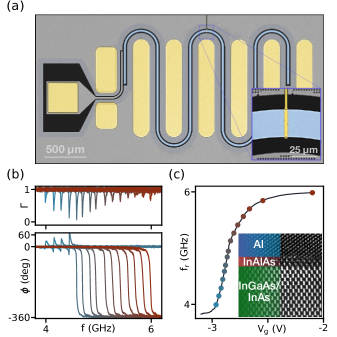
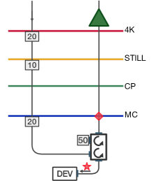
The JoFET amplifier is implemented as a half-wave coplanar waveguide (CPW) resonator with a gated superconductor-semiconductor hybrid Josephson field-effect-transistor positioned at the voltage node [Fig. 1(a)]. Ground planes of the device are formed from thin film Nb with -squared flux-pinning holes near the edges to improve magnetic-field resilience Samkharadze et al. (2016); Kroll et al. (2019). The entire center pin of the resonator is made of Al-InAs heterostructure, defined by chemical etch. The JoFET is defined by selective removal of the Al, followed by atomic layer deposition of alumina, and finally an electrostatic gate is defined with electron beam lithography and Au evaporation. Large Au chip-to-chip bond pads are also co-deposited in the final step to improve wire-bonding yield. The characteristic impedance of the CPW is designed to be near with wide center conductor width and a gap to the ground plane. The device is capacitively coupled to an open transmission line, which forms the only measurement port.
We targeted a geometric resonant frequency of approximately for compatibility with the standard band used in circuit quantum electrodynamics experiments. In designing the circuit, it is important to account for the kinetic inductance of the Al-InAs heterostructure, which in previous work caused a 20% reduction in the circuit resonant frequency Phan et al. (2022). The device is therefore designed with a geometric resonant frequency of , corresponding to a CPW resonator length of . We have not directly measured the kinetic contribution for this heterostructure growth, although we note that the Al is slightly thicker than the growth used in Ref. Phan et al. (2022) which should result in a relatively higher resonant frequency for the devices in this work.
The external coupling and the critical current determine the operating bandwidth and dynamic range of the amplifier Eichler and Wallraff (2014). While can be estimated from the circuit geometry, is more subtle because it depends on material details. Based on independent transport tests, we found that a JoFET with a width of have an expected critical current of at positive gate voltages. During design, we used Ref. Eichler and Wallraff (2014) to estimate that this critical current should yield a Kerr nonlinearity on the order of a few kHz. A more detailed discussion of the Kerr nonlinearity for our geometry and its relationship to critical current is given in Sec. IV. Based on the dynamic range calculation in Ref. Eichler and Wallraff (2014), a compression point of a few photons is expected when operating with of gain.
III Gate tunability
The complex microwave reflection coefficient of a small incident signal, with being the magnitude and being the phase, is measured from the sample in a dilution refrigerator with a standard measurement chain, including a cryogenic commercial high-electron mobility transistor amplifier (HEMT). For large (more positive) gate voltages, the measured reflection coefficient displays a small dip in magnitude and a winding of phase, signaling that the resonator is strongly coupled to the measurement port and that dissipation is weak [Fig. 1(b)]. Indeed, fitting the reflection coefficient to a one-port model gives an external coupling efficiency at zero gate voltage.
Application of negative gate voltage results in dramatic changes in resonator frequency [Fig. 1(b)], indicating that the JoFET contributes a gate-tunable inductance to the resonator. The resonant frequency can be tuned over more than of bandwidth [Fig. 1(c)], exhibiting weak voltage dependence at extremal values, reminiscent of a transistor reaching pinch-off at negative voltage and saturation at positive voltage.

The internal dissipation rate and external coupling rates also evolve with gate voltage. Near JoFET pinch off increases sharply, and decreases over the same range [Fig. 2(a),2(b)]. The net effect is therefore a decrease in coupling efficiency near pinch-off, which limits the usable frequency range of the JoFET amplifier.
A plausible origin of the increase in is dissipation in the JoFET region. To test this hypothesis, we consider a minimal model of the JoFET as a parallel resistor and inductor [Fig. 2(b),inset], and introduce an effective resistance where is the normalized flux drop across the resistor. The Josephson inductance and flux drop can be inferred from the measured resonant frequency if the bare circuit parameters without the Josephson junction are known (see Appendix C). In our case the bare circuit resonance is not precisely known because we have not characterized the heterostructure kinetic inductance for this particular material growth. We therefore model a range of possible bare resonant frequencies . The lower value of is taken from the resonant frequency at high gate voltage, and the upper value of is chosen to qualitatively match our measured Kerr nonlinearities, to be discussed later. The high-range value corresponds to a 10% reduction from the designed geometric resonance of , which, as one would expect, would imply that the current heterostructures have less kinetic inductance than those in our earlier studies on structures with thinner Al Phan et al. (2022).
Fitting to the circuit model results in agreement with the data, with a best-fit shunt resistance , where the uncertainty is derived from the possible range in . Based on this agreement, we conclude that the junction indeed introduces dissipation to the circuit, with the practical effect of limiting performance at high inductances. The microscopic origin of this dissipation is not understood. Candidate explanations are coupling to a lossy parasitic mode associated with the normal-conducting (Au) electrostatic gate, or a mechanism that is intrinsic to the Al-InAs material system. Turning now to external coupling, the simple RLC model captures gate dependence of at a qualitative level [Fig. 2(b)], although observed gate-dependence quantitatively exceeds theoretical expectations. This discrepancy may reflect the role of extra capacitance in the JoFET region introduced by the electrostatic gate, which is not accounted for in the model.
IV Nonlinearities and amplification
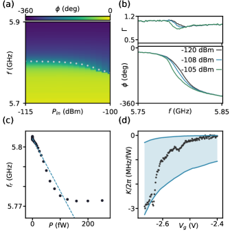
In addition to tunable inductance, the presence of the JoFET imparts a power-driven nonlinearity to the resonator Eichler and Wallraff (2014). Measuring the reflected phase as a function of signal frequency and power reveals that the resonant frequency smoothly decreases with increasing input power [Fig. 3(a)]. The output power from microwave sources is related to the resonator input power by an estimated total attenuation of for all measurements. The downward shift in resonant frequency is accompanied by “sharpening” of the phase response [Fig. 3(b)]. Downward shift in resonant frequency and an alteration in lineshape are key qualitative signatures of the required Kerr nonlinearity , which is useful for parametric amplification. The Kerr nonlinearity is estimated by measuring the change in resonant frequency per incident power in the low power limit, as shown by the linear fit in Fig. 3(c). Following this procedure at different gate voltages reveals that the nonlinearity is tunable with voltage, increasing in magnitude as gate voltage is decreased [Fig. 3(d)], qualitatively mirroring the decrease in circuit resonant frequency observed in Fig. 1(c). To make the relationship between the observed Kerr nonlinearity and the circuit parameters more concrete, we have estimated the expected Kerr nonlinearity based on our circuit model, using the formula for a low-transmission Josephson junction (shown in Fig. 3(d), see Appendix F for details). Unlike the case of linear circuit parameters, the uncertainty in the bare circuit resonance frequency () translates into many orders of magnitude of uncertainty in the Kerr nonlinearity, reflecting the fact that the Kerr nonlinearity is a fourth-order effect. Despite these challenges, our estimate indicates that the magnitude of the Kerr nonlinearity we observe is compatible with the circuit model considering this range of resonant frequencies. It is important to note that the formula that we compare with is valid only for low-transparency Josephson junctions, which is not the case for our system Kjaergaard et al. (2017); Mayer et al. (2019). If the bare circuit resonance were accurately known, a more complete treatment could possibly infer the true junction transparency based on the observed Kerr nonlinearity.
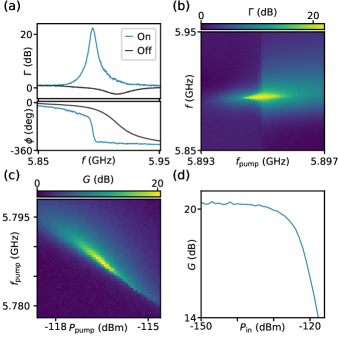
Parametric amplification is generated by applying a strong pump tone red detuned from the bare resonant frequency, in the vicinity of the phase “sharpening” features already identified close to the critical power [Fig. 3(b)]. Measuring scattering parameters with a weak probe signal reveals in excess of 20 dB of gain with a 4 MHz bandwidth, and a sharp phase response typical of a parametric amplifier [Fig. 4(a),4(b)]. Modest detunings in the pump frequency do not substantially affect the amplifier response, but for large deviations the gain decreases towards unity [Fig. 4(b)]. Measuring the amplifier gain as a function of pump frequency and input power reveals a continuous region of maximum gain with an easily identifiable optimum operating region, as expected for a parametric amplifier [Fig. 4(c)]. The gate voltages used for the gain optimization and measurement shown in Fig. 4(a),4(b) and in Fig. 4(c),4(d) are different due to gate instability, hysteresis, and shifts between cooldowns. These particular datasets were taken weeks apart, separated by many wide-range gate voltage sweeps, and in different cooldowns. Typically, after changing the gate voltage by a large amount (on the scale of Volts) it takes 15 minutes for the resonance to stabilize, and we find that there is hysteresis after large sweeps. In general the resonant frequency remains stable for circa an hour which is sufficient for our gain and noise measurements. After approximately one hour we often found measurable changes in amplifier gain and noise performance due to resonant frequency drifts, which could be compensated by re-optimization of the pump frequency and amplitude. We emphasize that the drifts in the resonant frequency over this time period are much smaller than the linewidth, but still noticeable when operating at high gain. We anticipate that optimization of the gate dielectric can greatly improve stability in future devices.
The power handling capability of the amplifier is quantified by measuring the gain for different signal powers [Fig. 4(d)]. At very low input signal power the gain saturates at [Fig. 4(d)]. Large input powers cause the amplifier gain to decrease, giving a compression point at input power of [Fig. 4(d)]. The gain and instantaneous bandwidth are comparable to early, parametric amplifiers based on metallic Al/AlOx Josephson junctions Castellanos-Beltran and Lehnert (2007); Castellanos-Beltran et al. (2008); Bergeal et al. (2010b). The frequency tunability of our resonator is also comparable to early parametric amplifiers Castellanos-Beltran and Lehnert (2007), although we have not demonstrated tunable amplification, which would currently be limited to the low-loss frequencies (see Figs. 1-2). The 1 dB compression point is only slightly lower than some early parametric amplifiers (two times below Ref. Zhou et al. (2014)), but orders of magnitude below modern implementations Macklin et al. (2015); Planat et al. (2020). Both the resonator loss and the compression point need to be significantly improved for this amplifier to be practically useful. In contrast to a recently-demonstrated semiconductor parametric amplifier with of gain Cochrane et al. (2022), our device has sufficient gain () to overwhelm the noise of later parts of the measurement chain.

Quantum signals typically consist of few photons, making it crucial to achieve noise performance near the quantum limit. To assess the noise performance of the JoFET amplifier, a weak pilot signal is measured first with a commercial HEMT amplifier, and then with parametric gain activated [Fig. 5(a)]. The JoFET amplifier dramatically improves the signal-to-noise ratio (SNR) of the pilot-signal measurement. Our calibration procedure, described in the next paragraph and in App. H, gives an indication that the total input-referred noise of the JoFET amplifier and subsequent measurement chain approaches the limits placed by quantum mechanics of one photon from nondegenerate amplification Caves (1982); Clerk et al. (2010). However, a definitive check of these results would require a calibrated noise source at device input. The excess noise in the device is consistent with expectations based on resonator loss and finite gain [purple tick in Fig. 5(a)], as derived from input-output theory in App. I.
This noise measurement was carefully calibrated by varying the temperature of the mixing-chamber stage of the dilution refrigerator and measuring noise at various frequencies with the JoFET amplifier off [Fig. 5(b)]. In the high temperature limit, the output noise is linear in temperature, with an intercept that reflects the added noise of the chain referred to the mixing chamber plate, giving at the JoFET operating frequency. At low temperature input-referred noise saturates. Calibrating over a wide range of frequencies reveals that noise saturation is pronounced only for high frequencies, consistent with the expected behavior for quantum fluctuations Clerk et al. (2010). This gives evidence that quantum fluctuations are faithfully resolved by our measurement chain. To find the noise referred to the JoFET input, , we measured insertion loss of all components in-between the JoFET input and the mixing chamber plate, and used these values to refer the noise spectra to the device input (see Appendix H). This calibration procedure counts resonator and sample-holder insertion loss against the performance of the JoFET amplifier, resulting in a noise temperature that represents the JoFET added noise referred to its input, which is a suitable quantity for characterizing the JoFET as a standalone device. It is not a measurement of total system efficiency, which would also need to include cable and circulator losses between a specified load and the JoFET.
Changing the pump frequency while keeping the signal frequency fixed at reveals that the noise performance is degraded if the pump frequency is away from the optimal operating region [Fig. 5(c)]. The change in noise performance with detuning matches the predictions of Eq. 17 with no free parameters [Fig. 5(c), purple line], indicating that the variation in noise performance is due to decreased gain. The level of agreement between experiment and theory in Fig. 5(c) gauges the accuracy of our noise calibration method, although we again emphasize that a calibrated noise source is needed for a definitive noise measurement. Note that this dataset was taken at a gate voltage with less resonator loss (), so the expected noise performance is somewhat better than in Fig. 5(a), but the data do not resolve this difference due to large propagated uncertainties in Fig. 5(c). By sweeping the pump frequency and the pump power with a fixed signal detuning, the optimum operating points of the amplifier can be extracted [Fig. 5(d)]. The operating points with best noise performance qualitatively correspond to the regions of highest gain identified in Fig. 4(c), as expected.
V Magnetic field operation
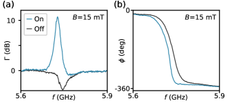
A general technical advantage conferred by the Al-InAs hybrid platform is compatibility with large, parallel external magnetic fields Pita-Vidal et al. (2020); Kringhøj et al. (2021); Phan et al. (2022). To explore if this advantage is realized in our particular device, we have steadily increased the parallel external magnetic field to while compensating for small field misalignments with a perpendicular magnetic coil. Even with compensation, the resonator parameters evolve slightly in magnetic field, and a slight increase in loss is observed. Applying a pump tone gives an optimized gain of [Fig. 6(a)-6(b)]. This demonstrates parametric amplification in a modest in-plane magnetic field, but far less than recently demonstrated high-field amplifiers Xu et al. (2022); Khalifa and Salfi (2022); Vine et al. (2022). Future experiments need to improve the resonator performance in magnetic field in order to allow a reliable noise measurement; we were unable to demonstrate quantum-limited operation in a magnetic field. The most likely reason for this is the depinning of trapped flux by high pump powers. This effect can be reduced by forming the resonator center pin from a field-compatible superconductor that connects to a smaller Al-InAs microstructure, as was done with recent field-compatible superconducting qubits Pita-Vidal et al. (2020); Kringhøj et al. (2021).
VI Outlook
Summarizing, we have demonstrated a high-performance JoFET amplifier, already obtaining performance comparable to early implementations in Al/AlOx material systems. A number of techniques are available to further improve the performance of our device. The participation factor of the superconductor-semiconductor heterostructure can be reduced drastically by working with a small mesa in the JoFET region. This would likely decrease microwave losses, and allow the use of field-resilient superconductors like NbTi, which should allow operations in external magnetic fields of order 1 Tesla. The number of JoFETs and the designed critical current can also be adapted to provide the target nonlinearity at milder gate voltages Eichler and Wallraff (2014). Device dissipation can also likely be improved by using a superconducting electrostatic gate with on-chip filters. Finally, superconducting-semiconducting hybrid material systems are being actively developed, so material-level improvements can be expected.
Our work opens up the new, general direction of quantum-limited signal processing devices based on semiconductors, and can be expanded to devices such as modulators Bergeal et al. (2010b); Chapman et al. (2017a) circulators Chapman et al. (2017b, 2019) or signal generators Cassidy et al. (2017). It is interesting to note that the electrostatic gate can be viewed as a receiver for high-impedance electrical signals, suggesting applications such as electrometry with an integrated, quantum-limited amplifier. Potential applications of electrometers include readout of spin qubits Chatterjee et al. (2021) and scanning-probe experiments Yoo et al. (1997); Ilani et al. (2001). Given the fact that this device uses a narrow-gap III/V semiconductor, it is also interesting to consider applications in photodetection.
Acknowledgements We thank Shyam Shankar for helpful feedback on the manuscript. We gratefully acknowledge the support of the ISTA nanofabrication facility, MIBA machine shop and e-machine shop. NYU team acknowledges support from Army Research Office grant no. W911NF2110303.
Data availability Raw data for all plots in the main text and supplement will be included with the manuscript before publication. Further data available upon reasonable request.
Appendix A Sample preparation
The JoFET amplifier was fabricated from Al-proximitized InAs quantum well which was grown on a semi-insulating, Fe counter-doped (100) InP wafer. Patterning was performed with a Raith EBPG 5100 electron beam lithography system. The Josephson weak link was made by etching a trench in the aluminum layer in the commercial etchant Transene D at for . The trench was designed to be long and wide. Scanning electron microscopy (SEM) later showed that the trench width was about . The superconductor-semiconductor mesa forming the center pin of the CPW resonator was formed by masking with polymethyl methacrylate (PMMA) followed by a semiconductor wet etch in a mixture of for 150 seconds at room temperature. The ground plane was constructed by evaporating Ti , Nb following a short 1-min Ar ion milling at an accelerating voltage of , with an ion current of in a Plassys ultra-high vacuum (UHV) evaporator. In the next step, the dielectric layer separating the gate and the junction was deposited with an Oxford atomic layer deposition (ALD) system running a thermal ALD alumina process at 150 degrees C in 150 cycles, which gave an approximated thickness of . Eventually, the gate that covers just the area of the Josephson weak link was created by evaporating Ti and Au at a tilt angle of 30 degrees with 5 RPM planetary rotation in a Plassys high vacuum (HV) evaporator. Due to low adhesion of Al bond wire to Nb ground plane, co-deposited Au bond pads are used to enhance Al alloy formation during wire bonding, hence, chip-to-chip bond yield. All lift-off and cleaning processes were performed in hot acetone at 50 degrees C and isopropanol.
The schematic in Fig. 7 shows cross section of the JoFET.

Appendix B Measurements
The sample was mounted on a copper bracket on a home made printed circuit board. We used a vector network analyzer (VNA) model Keysight P9372A to measure scattering parameters. A Rohde & Schwarz (R&S) signal generator model SGS100A was used to provide the pump tone. When pumping at a fixed frequency, we used the VNA to provide a small probe signal and measure the gain profile from the reflected monotone at probe frequency. A custom built low-noise voltage source provided the gate bias. To achieve gain, we typically set the gate voltage to and swept the VNA power until the response became critical. A pump tone from a R&S signal generator was injected at a power of about below the approximated critical power and slightly above the critical frequency. The probe power from the VNA was reduced to maintain the validity of the stiff pump condition. We tuned up the JoFET amplifier by sweeping the pump frequency and power in the proximity of the nonlinear resonator’s critical values and recording the maximal reflected amplitude at the VNA input. Optimal amplification configurations were then found by fine sweeping around the regions where the maximal gains were highest, whose values were typically more than . To measure the noise, we recorded the power spectral density from the output of the JoFET amplifier by a ThinkRF R5550 hybrid spectrum analyzer. In-plane magnetic field and compensation was applied by a vector magnet system of the Oxford Triton fridge and Mercury iPS power supply.
Appendix C RLC circuit model
To model gate-dependence of and in Fig. 2 we find an effective lumped-element representation of the circuit, and then couple it to transmission lines following the procedure in Ref. Göppl et al. (2008).
Our circuit can be imagined as two resonators of length and inductance per unit length , capacitance per unit length , and attenuation constant coupled through the parallel RL circuit. For a large shunt resistance the inductance of the parallel combination is given by . In this limit the model therefore introduces dissipation without substantially altering the resonant frequency. The resonant wave vector satisfies Bourassa et al. (2012)
| (1) |
The effective capacitance is Eichler and Wallraff (2014)
| (2) |
This expression arises from equating the capacitive energy in both resonators with an equivalent lumped-element energy , where is a flux normal mode with wave vector Bourassa et al. (2012); Eichler and Wallraff (2014).
We do not know of an explicit treatment of dissipation in our geometry available in the literature, so we seek an effective resistance in analogy with the effective capacitance discussed above. The Rayleigh dissipation function, which entirely determines the effect of the resistance on circuit dynamics Goldstein et al. (2011), is ), where is the flux drop across the resistor. This has the physical interpretation of 1/2 of the dissipated electrical power. Equating the dissipation function with an effective lumped-element dissipation rate suggests an effective resistance , where is the normalized flux drop across the resistor. Working in an effective lumped-element circuit model Göppl et al. (2008), we then add in parallel with the resonator dissipation, finding expressions for the total dissipation and coupling rates,
| (3) | |||||
| (4) |
where is the effective parallel resistance from the measurement port with impedance coupled with capacitance .
To fit this model we use the fact that where is the bare resonant frequency of the CPW resonator when is zero. As discussed in the main text, due to our uncertainty over how much inductance the junction contributes at large gate voltage we consider a range and then extract directly from the measured data. We fix the characteristic impedance of the resonator as based on the ratio between the designed geometric resonance frequency and the actual bare resonant frequency , which physically originates from the kinetic inductance of the heterostructure Phan et al. (2022). Knowledge of , , and allows the effective capacitance and Josephson inductance to be calculated. Eq. 3 is fit for and in Fig. 2(a) and Eq. (4) is fit for .
Appendix D Conversion from signal power to average intracavity photon number
The average intra-cavity photon number is linearly dependent on the incident power at the input port:
| (5) |
The input power is estimated based on the VNA power and the total attenuation of the setup. This is used when expressing the theoretical Kerr nonlinearity as a frequency shift per input power (MHz/fW) in Fig. 3(d).
Appendix E Total attenuation estimate
The total attenuation between the output of the VNA and the input of the device is calculated from noise spectrum from the measurement port with a signal tone at output power. The noise floor is identified with input-referred noise temperature from the HEMT calibration measurement shown in Fig. 5(b), combined with the resolution bandwidth of the signal analyzer , giving . The signal is above the noise floor, so its input referred magnitude is . Accounting for the small of loss from the (detuned) cavity then gives the total attenuation quoted in the main text. This value is compatible with expectations based on our installed attenuators and stainless steel cryogenic coaxial cables (estimated ), and room temperature components ().
Appendix F Kerr nonlinearity extraction from power sweep
The dependence of resonance frequency on input power was used to estimate the Kerr nonlinearity similar to Castellanos-Beltran and Lehnert (2007). Resonant frequency decreased linearly with increasing average intracavity photon number following the Hamiltonian Eichler and Wallraff (2014):
| (6) |
The slope of the line in Fig. 3(c) measures .
For low-transmission Josephson junctions, there is a fixed relationship between the Josephson energy and the Kerr nonlinearity Bourassa et al. (2012); Eichler and Wallraff (2014)
| (7) |
where is the effective inductance and is the normalized flux drop across the junction. We use this formula in Fig. 3(d).
Appendix G JoFET amplifier design
CPW resonator was designed to have a characteristic impedance of with the center conductor width and gap of and . Resonator length was chosen so that the target resonant frequency of would be achieved at base temperature. To account for the kinetic inductance of the 10 -thick Al layer, geometric resonant frequency was designed to be so that result resonance would drop to based on previous fabrication experience. The kinetic inductance of the Al film fluctuates from device to device, presumably due to uncontrolled oxidation of the Al. The JoFET was designed for a maximal critical current of which gives a zeroth order Kerr nonlinearity of at zero bias and in this CPW configuration, such that the device can be gated into a regime appropriate for amplification Eichler and Wallraff (2014). Designed dimensions were chosen based on our previous lithography tests and critical current measurements where a sheet critical current density of was achieved.
Appendix H JoFET input noise referral
The temperature sweep in Fig. 5(b) is used to refer HEMT noise to the mixing chamber plate [point in Fig. 8]. Noise is then referred to device input [point in Fig. 8] by measuring the transmission of the components in the signal path: the circulators, coaxial cables, sample board, and device Castellanos-Beltran and Lehnert (2007). We model this total loss as being from a beamsplitter with efficiency Palomaki et al. (2013).

The noise referred to , , is related to the real input noise at , , according to , where the second term represents the introduction of vacuum noise by loss. The total noise referred to point is then
| (8) |
which in the special case of vacuum-noise input gives .
There are two important cases in the experiment: the measurement with the JoFET amplifier off [black line, Fig. 5(a)], and the measurement with the JoFET amplifier on [blue line, Fig. 5(a)]. In the off state, the pilot tone is not on resonance with the cavity, but still experiences a small loss because of finite detuning. In addition to cavity loss, there is an imperfect system transmission from the components between and : the sample board, the circulators, and the coaxial cables. This results in a net transmission in the off state of
| (9) |
In the on state, there is a net gain from the device and the same system loss, so the net transmission in the on state is
| (10) |
Note that, according to this definition, is the net gain of the amplifier including any cavity losses when it is on.
Input-referred noise is found by substituting into Eq. (8) in the on case, and in the off case. Below we discuss how the three key parameters , , and are measured.
We found by measuring the transmission through our cryostat at a base temperature with and without the cable/circulator combination [ from Fig. 9], and also directly measured the sample holder insertion loss to be at liquid nitrogen temperatures. These losses combine to give our system loss .
We found from measured scattering parameters in the same configuration, taking into account the detuning of the pilot from circuit resonance. We emphasize that this number only includes a contribution from the circuit’s off-resonant insertion loss, but not any system components such as the sample holder.
Appendix I Expected noise performance

The quantum limit for phase-insensitive amplification is of input-referred added noise, where is the noise due to zero-point vacuum fluctuations Caves (1982). Losses and finite gain cause deviations from this limit. Here we determine the expected noise performance of our JoFET amplifier accounting for these effects.
We begin with the input-output relations for a Josephson parametric amplifier with input mode , output mode at a detuning from the pump frequency Eichler and Wallraff (2014),
| (12) |
The bath mode is required by the fluctuation-dissipation relation in the presence of nonzero loss. The complex signal gain is identically the scattering parameter , and the idler gain ensures that satisfies bosonic commutations relations Clerk et al. (2010). These commutation relations imply that
| (13) |
Assuming for convenience that the bath and idler modes are in their ground state with power spectral density , the output spectral density of the JoFET amplifier can be related to the input spectral density using Eq. 12,
| (14) |
Eliminating using Eq. 13 input referring by dividing out the gain gives , where the input-referred noise added by the JoFET amplifier is
| (15) |
This expression represents the input-referred added noise of the JoFET amplifier accounting for both finite gain and resonator loss. The first term is the quantum limit on added noise. The second term gives the corrections due to resonator loss. The final term gives a loss-independent correction for finite gain. In the high-gain limit, Eq. 15 reduces to a limiting value
| (16) |
which can be interpreted as the quantum limit plus unavoidable vacuum fluctuations arising from loss at the cavity input. Equation 16 is sometimes referred to as the device quantum limit Tóth et al. (2017).
As a check of Eq. 15, one can substitute , corresponding to the case where the amplifier is off and noise is measured at cavity resonance, and , corresponding to vacuum-noise input. In this case one finds that the output noise is also vacuum, , as expected.
To include the effect of system losses followed by our classical chain with temperature , we combine Eq. 15 with a simple beamsplitter noise model, as indicated in Fig. 10. The total input-referred noise of the model at small detunings where the gain is real, , is
| (17) |
Inserting along with the measured device parameters and system loss from App. H gives a total expected input-referred noise of for the data in Fig. 5(a) (indicated by purple tick right axis). Eq. 17 is also used to calculate the expected noise performance in Fig. 5(c).
Appendix J Repeatability of calibration data
The reproducibility of our circulator and cable insertion-loss measurements is key for the calibration described in App. H. To check the stability of our method, more than one week after calibrating we removed the circulators and cables and repeated our through calibration measurement [Fig. 11(a)]. The two measurements differ by less than over the relevant frequency range, with an average difference of . Since our calibration occurred over a timespan of a few days, we interpret the value measured over one week as a conservative bound on drifts during our calibration procedure. We therefore included an additional of uncertainty in the error bars in Figs. 5(a),5(c).
The calibrated components are inserted/removed via a bottom-loading exchange mechanism, which avoids having to thermally cycle the whole system. We suspect that this feature greatly improves the reproducibility of our method.

Appendix K Summary of datasets
Here we summarize the different datasets used in this work to facilitate their comparison.
Circuit characterization: A single continuous dataset is used for Figs. 1-2. A single dataset is used to demonstrate circuit nonlinearities in Fig. 3(a)-3(c). The nonlinearity is then characterized as a function of gate voltage in another dataset in Fig. 3(d). We checked that the circuit resonant frequencies in Fig. 3(d) are compatible with those in Fig. 1(c).
Amplifier characterization: A single dataset was used to show typical dependence of scattering parameters on pump power in Fig. 4(a)-4(b). Consecutive datasets at a nearby ( lower) gate voltage were then used to characterize the dependence of gain [Fig. 4(c)] and signal-to-noise ratio [Fig. 5(c),5(d)] on pump power and frequency. The key amplifier metrics of input-referred noise [Fig. 5(a)] and compression point [Fig. 4(d)] were measured consecutively. Noise was measured first, and compression point was measured at the same gate voltage approximately five hours later. HEMT calibration in Fig. 5(b) was performed the following day.
References
- Haus and Mullen (1962) H. A. Haus and J. A. Mullen, “Quantum noise in linear amplifiers,” Phys. Rev. 128, 2407–2413 (1962).
- Caves (1982) Carlton M. Caves, “Quantum limits on noise in linear amplifiers,” Phys. Rev. D 26, 1817–1839 (1982).
- Clerk et al. (2010) A. A. Clerk, M. H. Devoret, S. M. Girvin, Florian Marquardt, and R. J. Schoelkopf, “Introduction to quantum noise, measurement, and amplification,” Rev. Mod. Phys. 82, 1155–1208 (2010).
- Yurke et al. (1989) B. Yurke, L. R. Corruccini, P. G. Kaminsky, L. W. Rupp, A. D. Smith, A. H. Silver, R. W. Simon, and E. A. Whittaker, “Observation of parametric amplification and deamplification in a josephson parametric amplifier,” Phys. Rev. A 39, 2519–2533 (1989).
- Movshovich et al. (1990) R. Movshovich, B. Yurke, P. G. Kaminsky, A. D. Smith, A. H. Silver, R. W. Simon, and M. V. Schneider, “Observation of zero-point noise squeezing via a josephson-parametric amplifier,” Phys. Rev. Lett. 65, 1419–1422 (1990).
- Yurke et al. (1996) B. Yurke, M. L. Roukes, R. Movshovich, and A. N. Pargellis, “A low‐noise series‐array josephson junction parametric amplifier,” Applied Physics Letters 69, 3078–3080 (1996), https://doi.org/10.1063/1.116845 .
- Castellanos-Beltran and Lehnert (2007) M. A. Castellanos-Beltran and K. W. Lehnert, “Widely tunable parametric amplifier based on a superconducting quantum interference device array resonator,” Applied Physics Letters 91, 083509 (2007), https://doi.org/10.1063/1.2773988 .
- Castellanos-Beltran et al. (2008) M. A. Castellanos-Beltran, K. D. Irwin, G. C. Hilton, L. R. Vale, and K. W. Lehnert, “Amplification and squeezing of quantum noise with a tunable josephson metamaterial,” Nature Physics 4, 929–931 (2008).
- Bergeal et al. (2010a) N. Bergeal, F. Schackert, M. Metcalfe, R. Vijay, V. E. Manucharyan, L. Frunzio, D. E. Prober, R. J. Schoelkopf, S. M. Girvin, and M. H. Devoret, “Phase-preserving amplification near the quantum limit with a josephson ring modulator,” Nature 465, 64–68 (2010a).
- Macklin et al. (2015) C. Macklin, K. O’Brien, D. Hover, M. E. Schwartz, V. Bolkhovsky, X. Zhang, W. D. Oliver, and I. Siddiqi, “A near-quantum-limited josephson traveling-wave parametric amplifier,” Science 350, 307–310 (2015), https://www.science.org/doi/pdf/10.1126/science.aaa8525 .
- Planat et al. (2020) Luca Planat, Arpit Ranadive, Rémy Dassonneville, Javier Puertas Martínez, Sébastien Léger, Cécile Naud, Olivier Buisson, Wiebke Hasch-Guichard, Denis M. Basko, and Nicolas Roch, “Photonic-crystal josephson traveling-wave parametric amplifier,” Phys. Rev. X 10, 021021 (2020).
- Frattini et al. (2018) N. E. Frattini, V. V. Sivak, A. Lingenfelter, S. Shankar, and M. H. Devoret, “Optimizing the nonlinearity and dissipation of a snail parametric amplifier for dynamic range,” Phys. Rev. Applied 10, 054020 (2018).
- Butseraen et al. (2022) Guilliam Butseraen, Arpit Ranadive, Nicolas Aparicio, Kazi Rafsanjani Amin, Abhishek Juyal, Martina Esposito, Kenji Watanabe, Takashi Taniguchi, Nicolas Roch, François Lefloch, and Julien Renard, “A gate-tunable graphene josephson parametric amplifier,” Nature Nanotechnology 17, 1153–1158 (2022).
- Sarkar et al. (2022) Joydip Sarkar, Kishor V. Salunkhe, Supriya Mandal, Subhamoy Ghatak, Alisha H. Marchawala, Ipsita Das, Kenji Watanabe, Takashi Taniguchi, R. Vijay, and Mandar M. Deshmukh, “Quantum-noise-limited microwave amplification using a graphene josephson junction,” Nature Nanotechnology 17, 1147–1152 (2022).
- Shabani et al. (2016) J. Shabani, M. Kjaergaard, H. J. Suominen, Younghyun Kim, F. Nichele, K. Pakrouski, T. Stankevic, R. M. Lutchyn, P. Krogstrup, R. Feidenhans’l, S. Kraemer, C. Nayak, M. Troyer, C. M. Marcus, and C. J. Palmstrøm, “Two-dimensional epitaxial superconductor-semiconductor heterostructures: A platform for topological superconducting networks,” Phys. Rev. B 93, 155402 (2016).
- Sarney et al. (2018) Wendy L. Sarney, Stefan P. Svensson, Kaushini S. Wickramasinghe, Joseph Yuan, and Javad Shabani, “Reactivity studies and structural properties of al on compound semiconductor surfaces,” Journal of Vacuum Science & Technology B 36, 062903 (2018), https://doi.org/10.1116/1.5053987 .
- Sarney et al. (2020) Wendy L. Sarney, Stefan P. Svensson, Asher C. Leff, William F. Schiela, Joseph O. Yuan, Matthieu C. Dartiailh, William Mayer, Kaushini S. Wickramasinghe, and Javad Shabani, “Aluminum metallization of iii–v semiconductors for the study of proximity superconductivity,” Journal of Vacuum Science & Technology B 38, 032212 (2020), https://doi.org/10.1116/1.5145073 .
- Kjaergaard et al. (2016) M. Kjaergaard, F. Nichele, H. J. Suominen, M. P. Nowak, M. Wimmer, A. R. Akhmerov, J. A. Folk, K. Flensberg, J. Shabani, C. J. Palmstrøm, and C. M. Marcus, “Quantized conductance doubling and hard gap in a two-dimensional semiconductor–superconductor heterostructure,” Nature Communications 7, 12841 (2016).
- Mayer et al. (2019) William Mayer, Joseph Yuan, Kaushini S. Wickramasinghe, Tri Nguyen, Matthieu C. Dartiailh, and Javad Shabani, “Superconducting proximity effect in epitaxial al-inas heterostructures,” Applied Physics Letters 114, 103104 (2019).
- Dartiailh et al. (2021a) Matthieu C. Dartiailh, Joseph J. Cuozzo, Bassel H. Elfeky, William Mayer, Joseph Yuan, Kaushini S. Wickramasinghe, Enrico Rossi, and Javad Shabani, “Missing shapiro steps in topologically trivial josephson junction on InAs quantum well,” Nature Communications 12, 78 (2021a).
- Nichele et al. (2017) Fabrizio Nichele, Asbjørn C. C. Drachmann, Alexander M. Whiticar, Eoin C. T. O’Farrell, Henri J. Suominen, Antonio Fornieri, Tian Wang, Geoffrey C. Gardner, Candice Thomas, Anthony T. Hatke, Peter Krogstrup, Michael J. Manfra, Karsten Flensberg, and Charles M. Marcus, “Scaling of majorana zero-bias conductance peaks,” Phys. Rev. Lett. 119, 136803 (2017).
- Fornieri et al. (2019) Antonio Fornieri, Alexander M. Whiticar, F. Setiawan, Elías Portolés, Asbjørn C. C. Drachmann, Anna Keselman, Sergei Gronin, Candice Thomas, Tian Wang, Ray Kallaher, Geoffrey C. Gardner, Erez Berg, Michael J. Manfra, Ady Stern, Charles M. Marcus, and Fabrizio Nichele, “Evidence of topological superconductivity in planar josephson junctions,” Nature 569, 89–92 (2019).
- Dartiailh et al. (2021b) Matthieu C. Dartiailh, William Mayer, Joseph Yuan, Kaushini S. Wickramasinghe, Alex Matos-Abiague, Igor Žutić, and Javad Shabani, “Phase signature of topological transition in josephson junctions,” Phys. Rev. Lett. 126, 036802 (2021b).
- Aghaee et al. (2022) Morteza Aghaee, Arun Akkala, Zulfi Alam, Rizwan Ali, Alejandro Alcaraz Ramirez, Mariusz Andrzejczuk, Andrey E Antipov, Pavel Aseev, Mikhail Astafev, Bela Bauer, Jonathan Becker, Srini Boddapati, Frenk Boekhout, Jouri Bommer, Esben Bork Hansen, Tom Bosma, Leo Bourdet, Samuel Boutin, Philippe Caroff, Lucas Casparis, Maja Cassidy, Anna Wulf Christensen, Noah Clay, William S Cole, Fabiano Corsetti, Ajuan Cui, Paschalis Dalampiras, Anand Dokania, Gijs de Lange, Michiel de Moor, Juan Carlos Estrada Saldaña, Saeed Fallahi, Zahra Heidarnia Fathabad, John Gamble, Geoff Gardner, Deshan Govender, Flavio Griggio, Ruben Grigoryan, Sergei Gronin, Jan Gukelberger, Sebastian Heedt, Jesús Herranz Zamorano, Samantha Ho, Ulrik Laurens Holgaard, William Hvidtfelt Padkær Nielsen, Henrik Ingerslev, Peter Jeppesen Krogstrup, Linda Johansson, Jeffrey Jones, Ray Kallaher, Farhad Karimi, Torsten Karzig, Cameron King, Maren Elisabeth Kloster, Christina Knapp, Dariusz Kocon, Jonne Koski, Pasi Kostamo, Mahesh Kumar, Tom Laeven, Thorvald Larsen, Kongyi Li, Tyler Lindemann, Julie Love, Roman Lutchyn, Michael Manfra, Elvedin Memisevic, Chetan Nayak, Bas Nijholt, Morten Hannibal Madsen, Signe Markussen, Esteban Martinez, Robert McNeil, Andrew Mullally, Jens Nielsen, Anne Nurmohamed, Eoin O’Farrell, Keita Otani, Sebastian Pauka, Karl Petersson, Luca Petit, Dima Pikulin, Frank Preiss, Marina Quintero Perez, Katrine Rasmussen, Mohana Rajpalke, Davydas Razmadze, Outi Reentila, David Reilly, Richard Rouse, Ivan Sadovskyy, Lauri Sainiemi, Sydney Schreppler, Vadim Sidorkin, Amrita Singh, Shilpi Singh, Sarat Sinha, Patrick Sohr, Tomaš Stankevič, Lieuwe Stek, Henri Suominen, Judith Suter, Vicky Svidenko, Sam Teicher, Mine Temuerhan, Nivetha Thiyagarajah, Raj Tholapi, Mason Thomas, Emily Toomey, Shivendra Upadhyay, Ivan Urban, Saulius Vaitiekėnas, Kevin Van Hoogdalem, Dmitrii V. Viazmitinov, Steven Waddy, David Van Woerkom, Dominik Vogel, John Watson, Joseph Weston, Georg W. Winkler, Chung Kai Yang, Sean Yau, Daniel Yi, Emrah Yucelen, Alex Webster, Roland Zeisel, and Ruichen Zhao, “Inas-al hybrid devices passing the topological gap protocol,” arXiv:2207.02472 (2022).
- Bøttcher et al. (2018) C. G. L. Bøttcher, F. Nichele, M. Kjaergaard, H. J. Suominen, J. Shabani, C. J. Palmstrøm, and C. M. Marcus, “Superconducting, insulating and anomalous metallic regimes in a gated two-dimensional semiconductor–superconductor array,” Nature Physics 14, 1138–1144 (2018).
- Casparis et al. (2018) Lucas Casparis, Malcolm R. Connolly, Morten Kjaergaard, Natalie J. Pearson, Anders Kringhøj, Thorvald W. Larsen, Ferdinand Kuemmeth, Tiantian Wang, Candice Thomas, Sergei Gronin, Geoffrey C. Gardner, Michael J. Manfra, Charles M. Marcus, and Karl D. Petersson, “Superconducting gatemon qubit based on a proximitized two-dimensional electron gas,” Nature Nanotechnology 13, 915–919 (2018).
- Phan et al. (2022) D. Phan, J. Senior, A. Ghazaryan, M. Hatefipour, W. M. Strickland, J. Shabani, M. Serbyn, and A. P. Higginbotham, “Detecting induced pairing at the al-inas interface with a quantum microwave circuit,” Phys. Rev. Lett. 128, 107701 (2022).
- Pita-Vidal et al. (2020) Marta Pita-Vidal, Arno Bargerbos, Chung-Kai Yang, David J. van Woerkom, Wolfgang Pfaff, Nadia Haider, Peter Krogstrup, Leo P. Kouwenhoven, Gijs de Lange, and Angela Kou, “Gate-tunable field-compatible fluxonium,” Phys. Rev. Appl. 14, 064038 (2020).
- Kringhøj et al. (2021) A. Kringhøj, T. W. Larsen, O. Erlandsson, W. Uilhoorn, J.G. Kroll, M. Hesselberg, R.P.G. McNeil, P. Krogstrup, L. Casparis, C.M. Marcus, and K.D. Petersson, “Magnetic-field-compatible superconducting transmon qubit,” Phys. Rev. Applied 15, 054001 (2021).
- Xu et al. (2022) Mingrui Xu, Risheng Cheng, Yufeng Wu, Gangqiang Liu, and Hong X.Tang, “Magnetic field-resilient quantum-limited parametric amplifier,” arXiv:2209.13652 (2022).
- Khalifa and Salfi (2022) M. Khalifa and J. Salfi, “Nonlinearity and parametric amplification of superconducting nanowire resonators in magnetic field,” arXiv:2209.14523 (2022).
- Vine et al. (2022) Wyatt Vine, Mykhailo Savytskyi, Daniel Parker, James Slack-Smith, Thomas Schenkel, Jeffrey C. McCallum, Brett C. Johnson, Andrea Morello, and Jarryd J. Pla, “In-situ amplification of spin echoes within a kinetic inductance parametric amplifier,” arXiv:2211.11333 (2022).
- Schaal et al. (2019) Simon Schaal, Alessandro Rossi, Virginia N. Ciriano-Tejel, Tsung-Yeh Yang, Sylvain Barraud, John J. L. Morton, and M. Fernando Gonzalez-Zalba, “A cmos dynamic random access architecture for radio-frequency readout of quantum devices,” Nature Electronics 2, 236–242 (2019).
- Pauka et al. (2021) S. J. Pauka, K. Das, R. Kalra, A. Moini, Y. Yang, M. Trainer, A. Bousquet, C. Cantaloube, N. Dick, G. C. Gardner, M. J. Manfra, and D. J. Reilly, “A cryogenic cmos chip for generating control signals for multiple qubits,” Nature Electronics 4, 64–70 (2021).
- Xue et al. (2021) Xiao Xue, Bishnu Patra, Jeroen P. G. van Dijk, Nodar Samkharadze, Sushil Subramanian, Andrea Corna, Brian Paquelet Wuetz, Charles Jeon, Farhana Sheikh, Esdras Juarez-Hernandez, Brando Perez Esparza, Huzaifa Rampurawala, Brent Carlton, Surej Ravikumar, Carlos Nieva, Sungwon Kim, Hyung-Jin Lee, Amir Sammak, Giordano Scappucci, Menno Veldhorst, Fabio Sebastiano, Masoud Babaie, Stefano Pellerano, Edoardo Charbon, and Lieven M. K. Vandersypen, “Cmos-based cryogenic control of silicon quantum circuits,” Nature 593, 205–210 (2021).
- Lecocq et al. (2021) F. Lecocq, F. Quinlan, K. Cicak, J. Aumentado, S. A. Diddams, and J. D. Teufel, “Control and readout of a superconducting qubit using a photonic link,” Nature 591, 575–579 (2021).
- Cochrane et al. (2022) Laurence Cochrane, Theodor Lundberg, David J. Ibberson, Lisa A. Ibberson, Louis Hutin, Benoit Bertrand, Nadia Stelmashenko, Jason W. A. Robinson, Maud Vinet, Ashwin A. Seshia, and M. Fernando Gonzalez-Zalba, “Parametric amplifiers based on quantum dots,” Phys. Rev. Lett. 128, 197701 (2022).
- Larsen et al. (2015) T. W. Larsen, K. D. Petersson, F. Kuemmeth, T. S. Jespersen, P. Krogstrup, J. Nygård, and C. M. Marcus, “Semiconductor-nanowire-based superconducting qubit,” Phys. Rev. Lett. 115, 127001 (2015).
- Veldhorst et al. (2014) M. Veldhorst, J. C. C. Hwang, C. H. Yang, A. W. Leenstra, B. de Ronde, J. P. Dehollain, J. T. Muhonen, F. E. Hudson, K. M. Itoh, A. Morello, and A. S. Dzurak, “An addressable quantum dot qubit with fault-tolerant control-fidelity,” Nature Nanotechnology 9, 981–985 (2014).
- Takeda et al. (2016) Kenta Takeda, Jun Kamioka, Tomohiro Otsuka, Jun Yoneda, Takashi Nakajima, Matthieu R. Delbecq, Shinichi Amaha, Giles Allison, Tetsuo Kodera, Shunri Oda, and Seigo Tarucha, “A fault-tolerant addressable spin qubit in a natural silicon quantum dot,” Science Advances 2, e1600694 (2016), https://www.science.org/doi/pdf/10.1126/sciadv.1600694 .
- Yoneda et al. (2018) Jun Yoneda, Kenta Takeda, Tomohiro Otsuka, Takashi Nakajima, Matthieu R. Delbecq, Giles Allison, Takumu Honda, Tetsuo Kodera, Shunri Oda, Yusuke Hoshi, Noritaka Usami, Kohei M. Itoh, and Seigo Tarucha, “A quantum-dot spin qubit with coherence limited by charge noise and fidelity higher than 99.9%,” Nature Nanotechnology 13, 102–106 (2018).
- Noiri et al. (2022) Akito Noiri, Kenta Takeda, Takashi Nakajima, Takashi Kobayashi, Amir Sammak, Giordano Scappucci, and Seigo Tarucha, “Fast universal quantum gate above the fault-tolerance threshold in silicon,” Nature 601, 338–342 (2022).
- Xue et al. (2022) Xiao Xue, Maximilian Russ, Nodar Samkharadze, Brennan Undseth, Amir Sammak, Giordano Scappucci, and Lieven M. K. Vandersypen, “Computing with spin qubits at the surface code error threshold,” arXiv:2107.00628 (2022).
- Samkharadze et al. (2016) N. Samkharadze, A. Bruno, P. Scarlino, G. Zheng, D. P. DiVincenzo, L. DiCarlo, and L. M. K. Vandersypen, “High-kinetic-inductance superconducting nanowire resonators for circuit qed in a magnetic field,” Phys. Rev. Applied 5, 044004 (2016).
- Kroll et al. (2019) J.G. Kroll, F. Borsoi, K.L. van der Enden, W. Uilhoorn, D. de Jong, M. Quintero-Pérez, D.J. van Woerkom, A. Bruno, S.R. Plissard, D. Car, E.P.A.M. Bakkers, M.C. Cassidy, and L.P. Kouwenhoven, “Magnetic-field-resilient superconducting coplanar-waveguide resonators for hybrid circuit quantum electrodynamics experiments,” Phys. Rev. Applied 11, 064053 (2019).
- Eichler and Wallraff (2014) Christopher Eichler and Andreas Wallraff, “Controlling the dynamic range of a josephson parametric amplifier,” EPJ Quantum Technology 1, 2 (2014).
- Kjaergaard et al. (2017) M. Kjaergaard, H. J. Suominen, M. P. Nowak, A. R. Akhmerov, J. Shabani, C. J. Palmstrøm, F. Nichele, and C. M. Marcus, “Transparent semiconductor-superconductor interface and induced gap in an epitaxial heterostructure josephson junction,” Phys. Rev. Appl. 7, 034029 (2017).
- Bergeal et al. (2010b) N. Bergeal, R. Vijay, V. E. Manucharyan, I. Siddiqi, R. J. Schoelkopf, S. M. Girvin, and M. H. Devoret, “Analog information processing at the quantum limit with a josephson ring modulator,” Nature Physics 6, 296–302 (2010b).
- Zhou et al. (2014) X. Zhou, V. Schmitt, P. Bertet, D. Vion, W. Wustmann, V. Shumeiko, and D. Esteve, “High-gain weakly nonlinear flux-modulated josephson parametric amplifier using a squid array,” Phys. Rev. B 89, 214517 (2014).
- Chapman et al. (2017a) Benjamin J. Chapman, Eric I. Rosenthal, Joseph Kerckhoff, Leila R. Vale, Gene C. Hilton, and K. W. Lehnert, “Single-sideband modulator for frequency domain multiplexing of superconducting qubit readout,” Applied Physics Letters 110, 162601 (2017a), https://doi.org/10.1063/1.4981390 .
- Chapman et al. (2017b) Benjamin J. Chapman, Eric I. Rosenthal, Joseph Kerckhoff, Bradley A. Moores, Leila R. Vale, J. A. B. Mates, Gene C. Hilton, Kevin Lalumière, Alexandre Blais, and K. W. Lehnert, “Widely tunable on-chip microwave circulator for superconducting quantum circuits,” Phys. Rev. X 7, 041043 (2017b).
- Chapman et al. (2019) Benjamin J. Chapman, Eric I. Rosenthal, and K. W. Lehnert, “Design of an on-chip superconducting microwave circulator with octave bandwidth,” Phys. Rev. Applied 11, 044048 (2019).
- Cassidy et al. (2017) M. C. Cassidy, A. Bruno, S. Rubbert, M. Irfan, J. Kammhuber, R. N. Schouten, A. R. Akhmerov, and L. P. Kouwenhoven, “Demonstration of an ac josephson junction laser,” Science 355, 939–942 (2017), https://www.science.org/doi/pdf/10.1126/science.aah6640 .
- Chatterjee et al. (2021) Anasua Chatterjee, Paul Stevenson, Silvano De Franceschi, Andrea Morello, Nathalie P. de Leon, and Ferdinand Kuemmeth, “Semiconductor qubits in practice,” Nature Reviews Physics 3, 157–177 (2021).
- Yoo et al. (1997) M. J. Yoo, T. A. Fulton, H. F. Hess, R. L. Willett, L. N. Dunkleberger, R. J. Chichester, L. N. Pfeiffer, and K. W. West, “Scanning single-electron transistor microscopy: Imaging individual charges,” Science 276, 579–582 (1997), https://www.science.org/doi/pdf/10.1126/science.276.5312.579 .
- Ilani et al. (2001) S. Ilani, A. Yacoby, D. Mahalu, and Hadas Shtrikman, “Microscopic structure of the metal-insulator transition in two dimensions,” Science 292, 1354–1357 (2001), https://www.science.org/doi/pdf/10.1126/science.1058645 .
- Göppl et al. (2008) M. Göppl, A. Fragner, M. Baur, R. Bianchetti, S. Filipp, J. M. Fink, P. J. Leek, G. Puebla, L. Steffen, and A. Wallraff, “Coplanar waveguide resonators for circuit quantum electrodynamics,” Journal of Applied Physics 104, 113904 (2008), https://doi.org/10.1063/1.3010859 .
- Bourassa et al. (2012) J. Bourassa, F. Beaudoin, Jay M. Gambetta, and A. Blais, “Josephson-junction-embedded transmission-line resonators: From kerr medium to in-line transmon,” Phys. Rev. A 86, 013814 (2012).
- Goldstein et al. (2011) Herber Goldstein, Charles P. Poole, and John L. Safko, Classical Mechanics, 3rd ed. (Pearson, 2011).
- Palomaki et al. (2013) T. A. Palomaki, J. D. Teufel, R. W. Simmonds, and K. W. Lehnert, “Entangling mechanical motion with microwave fields,” Science 342, 710–713 (2013), https://www.science.org/doi/pdf/10.1126/science.1244563 .
- Tóth et al. (2017) L. D. Tóth, N. R. Bernier, A. Nunnenkamp, A. K. Feofanov, and T. J. Kippenberg, “A dissipative quantum reservoir for microwave light using a mechanical oscillator,” Nature Physics 13, 787–793 (2017).