Quantum-well states at the surface of the heavy fermion superconductor URu2Si2
Electrons can form a two-dimensional electron gas at metal surfaces, where lateral confinement leads to quantum-well states. Such states have been observed for highly itinerant electrons, but it remains an open question whether quantum-well states can be formed from strongly correlated electrons. Here we study atomically flat terraces on surfaces of the heavy-fermion superconductor URu2Si2 using millikelvin scanning tunneling spectroscopy. We observe two-dimensional heavy fermions (2DHF) with an effective mass 17 times the free electron mass that form quantized states separated by a fraction of a meV. Superconductivity at the surface is induced by the bulk into the 2DHF. Our results provide a new route to realize quantum well states in correlated quantum materials.
Two-dimensional electronic states confined at surfaces are ubiquitously observed within the gaps of the bulk dispersion relation of metals opened by the periodic crystalline lattice (?, ?, ?, ?, ?, ?). These states can be further confined through scattering by features forming closed geometries at the surface, for example at a terrace between two surface steps. Then, quantized energy levels emerge, typically from itinerant electron states of the two-dimensional surface band (?, ?, ?). Their separation in energy is often of hundreds of meV, i.e. a few percent of the width of the surface band. Their lifetime (or the level width) is set by the interaction between the surface and bulk states and is slightly smaller than the level separation (?, ?, ?, ?, ?). Quantum well states form at the surface of many different materials and provide a fascinating ground to visualize electron correlations and study the influence of geometry or of adatoms and impurities (?, ?, ?, ?, ?, ?). However, it remains difficult to obtain quantum-well states whose separation in energy is in the meV range and thus comparable to bulk low energy phenomena, such as for example superconductivity. Increasing the spatial extension of the confinement potential could eventually lead to a reduction of the level separation. But the lifetime would then remain of the same order and the level width would increase well above the level separation. To reduce the level separation to the meV range one needs systems with a narrow band crossing the Fermi level. So called heavy-fermion metals provide such a flat band in the bulk due to collective Kondo hybridization. As a consequence of the increased density of states, these systems are highly susceptible to present exotic low temperature properties, as for example d-wave or triplet p-wave superconductivity (?, ?, ?, ?, ?, ?, ?, ?, ?, ?). It was found that reducing the dimensionality in heavy fermions leads to suppression of magnetism and to a deviation from standard Fermi liquid electronic interactions in certain superlattices of compounds with a layered crystalline structure (?). Furthermore, narrow surface bands with a Dirac dispersion were found in a semiconducting heavy fermion (?). However, two-dimensional heavy fermions (2DHF) have not been observed at surfaces of metallic compounds, and no quantum-well states due to lateral confinement have been realized. Here we show that 2DHF appear at the surface of a heavy fermion metal and that these form quantum well states at terraces between steps.
Bulk URu2Si2 exhibits correlated heavy electron bands crossing the Fermi level in the bulk (Fig. 1(A)) and shows a transition to a mysterious phase (called hidden order, HO) characterized among other features by the opening of a partial gap in the bandstructure below 17.5 K, out of which an unconventional superconducting state develops below 1.5 K (?, ?, ?). Its surface has been intensively investigated; there are electronic surface states with bands whose effective masses are mostly relatively small (?, ?, ?, ?). Here we use Scanning Tunneling Microscopy (STM) to investigate small-sized atomically flat terraces on the surface of URu2Si2. We observe 2DHF with an effective mass 17 times the free electron mass and quantization due to lateral confinement.
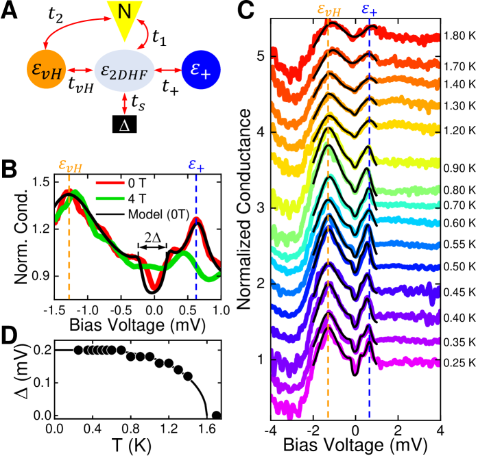
We present a STM image of terraces in URu2Si2 in Fig. 1(B). The bias voltage dependence of the tunneling conductance coincides with results obtained in previous STM work on flat surfaces, except for the features associated to the 2DHF discussed below (?, ?, ?, ?, ?). The shape and temperature dependence of the tunneling conductance shows band hybridization induced by electronic correlations and the formation of the heavy fermion state when cooling (Fig. 1(A)). In Fig. 1(C,D,E) we show results at three different temperatures (details provided in Supplementary Sections S1 and S2). At temperatures above (Fig. 1(C)) we observe a strong asymmetric Fano lineshape due to interfering simultaneous tunneling into localized f-electron and conduction electron states. Below (Fig. 1(D)), a gap opens around the Fermi level. Inside the gap, we observe a van Hove anomaly at meV due to the dispersion bending of the low energy bandstructure. These features were also found in previous work (?, ?, ?, ?, ?, ?). When cooling further (Fig. 1(E)), below the superconducting critical temperature K, we find a peak at meV and the superconducting gap with the value expected from and BCS theory, eV. We analyze in more detail the latter two features below.
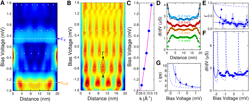
To discuss the observation of the quantized 2DHF, let us focus on the tunneling conductance along the white line shown in Fig. 1(B) for very low bias voltages, between 1.6 mV. Along this line, we identify four terraces of different sizes, nm, nm, nm and nm (Fig. 1(F)). We observe peaks in the tunneling conductance at meV and at meV all over the flat regions of the terraces (orange and blue arrows in Fig. 1(G)). At the steps, these features move into an edge state which we discuss below. There is a strong bias voltage and position dependence of the tunneling conductance which is different for each terrace. We show in Fig. 1(H) representative tunneling conductance curves at each terrace. For the larger terraces, and , we can identify a set of new peaks (vertical arrows in Fig. 1(H)).
To further understand these peaks, let us focus on the terrace , marked by a dashed rectangle in Fig. 1(B). We symmetrize the tunneling spectroscopy along the long axis of the terrace and show the resulting tunneling conductance in Fig. 2(A). We can identify a set of peaks in the tunneling conductance which evolve both in position and bias voltage. Removing the background introduced by the features at meV and at meV from the tunneling conductance (Fig. 1(E)) leads to the pattern shown in Fig. 2(B). We calculate the expected position of peaks from lateral quantization using interfering wavefunctions partially reflected at steps. The quantization pattern for confined electrons ressembles the Fabry-Pérot expression for an interferometer made by partially reflecting mirrors (?), with the reflection coefficient and the phase shift as free parameters (details in the Supplementary Section S3). The results are the white dots in Fig. 2(A,B), whose position coincides well with the peaks in the conductance pattern observed in the experiment. In Fig. 2(C) we plot as circles the position of the peaks as a function of the wavevector and as a line the dispersion relation , where is the effective mass and the bottom of the band. We obtain meV and , with the free electron mass, i.e., a massive electron state. A detailed comparison of the tunneling conductance vs. position with the square of wavefunctions confined by a lateral potential leads to excellent fits, shown in Fig. 2(D). The phase shift determines the position and energy of the peaks (white dots in Fig. 2(B)) and the best account of our observations is obtained with . We find values around 0.2, which slightly increase when approaching (Fig. 2(E)). The low value of is also found in simple metals, for example is between 0.2 and 0.4 in Ag and Cu (?, ?, ?). However, the energy dependence (Fig. 2(E)) is here completely different than in usual metals. While varies mildly in Cu or Ag in the range of a few eV (see discontinous line in Fig. 2(E) and Refs. (?, ?, ?)), here we observe instead that decreases markedly in a range of a few meV (points in Fig. 2(E)). We can reproduce the observed dependence of vs. bias voltage assuming a rectangular well of 20 nm size and a barrier with a height of 5 meV (blue line in Fig. 2(E)) (?, ?). It is also insightful to trace the tunneling conductance as a function of the bias voltage at the center of the terrace (Fig. 2(F)) and compare it to the expectation for (dashed line in Fig. 2(F)) and for (continuous line in Fig. 2(F)). We see that both the periodicity and shape are well explained by a reduced in an energy range of a few meV, i.e. two orders of magnitude below the energy range observed in normal metals (?, ?, ?, ?, ?, ?, ?, ?, ?).
To further investigate the quantized levels, we have fitted each peak (see black arrows in Fig. 2(B)) to a Lorentzian function, whose width (Fig. 2(B)) provides the lifetime (Fig. 2(G)) of the quantum well states. Taking a 2D electron gas, we expect with Å-1 the Thomas-Fermi screening length and the Fermi wavevector (?) (dashed line in Fig. 2(G)). Our data are not well reproduced by this expression. Instead taking with meV and eV (line in Fig. 2(G)) we find a much better account of our experiment (?, ?). This shows that the lifetime is set by the decay into bulk states. Quantum well states sense the bulk Fermi liquid correlations, given by the quadratic energy term in . This has been observed in surface states of noble metals, monolayers of Pb, and in Sb. However, in those cases the energy range was three orders of magnitude above the one we discuss here (?, ?, ?, ?, ?).
Using meV, obtained from the fit, we estimate the lifetime of the ground state as meV ps. Similarly, the lifetime of states close to the Fermi level is ps. We can also estimate a value for a mean free path, , taking for the Fermi velocity of URu2Si2. This value is of the same order of magnitude as those observed in ultraclean URu2Si2 single crystals reported in Ref. (?). Furthermore, the finite is related to the reflection coefficient , also due to electronic interactions with the bulk. The blue line in Fig. 2(E) assumes a single isolated quantum well and thus perfect reflection at . In the presence of many terraces, as we find in our experiment, we can consider multiple scattering events from different terraces (?, ?). Then, in the extrapolation of to , is given by , where is the terrace width (?). We find , which is consistent with the extrapolation of to meV from our data (dotted line in Fig. 2(E)).
To vindicate the heavy-fermion surface state we have performed Density Functional Theory (DFT) calculations of the surface bandstructure of a slab of URu2Si2 (Supplementary Section S4). We find a shallow, U derived f-electron band with a flat dispersion relation compatible to our experiments around the point of the simple tetragonal Brillouin zone. The bulk electronic spectrum is gapped in this part of the Brillouin zone (?, ?). The rest of the Brillouin zone provides surface states with much smaller effective masses.
It is important to see how the 2DHF is modified at steps and impurities. We discuss the behavior at steps here (providing more details provided in Supplementary Section S5). The behavior at impurities is provided in Supplementary Section S6. In the conductance map shown in Fig. 1(G) we find that the features in the tunneling conductance change their position in bias voltage as a whole when approaching a step. The peak due to the van Hove anomaly at meV and the peak at meV both vanish close to the steps. Instead we find a high peak at meV (see for example the red blobs at the sides of Fig. 2(A)). This indicates that the lateral quantized levels evolve at the step into 1D-Edge States (1DES) of the 2DHF. An 1DES is the result of charge accumulation at the step and a modified local electron density (?, ?, ?). A careful characterization of the feature at terraces of different sizes shows that the 1DES is always at the same distance from the step and has the same lateral size (Supplementary Section S5). Furthermore, a gap opens at the step and is filled at by the resonant 1DES.
This precise and succesful comparison between the observed tunneling conductance and all relevant features of a 2DHF, including quantized levels sensing the bulk correlations and the formation of edge states at steps, provides a neat picture of the surface of the heavy fermion URu2Si2—there are 2DHF at the surface which are connected to the bulk.
The question is now how does this situation impacts on the features in the tunneling conductance due to superconductivity. When we look on the energy range below the superconducting gap, eV, we remark that the superconducting features are strongly suppressed, with a large zero bias conductance. There are indications for unconventional superconductivity in bulk URu2Si2, for instance with d-wave symmetry order parameter (?). This can contribute to the suppression of the superconducting features, but it hardly leads to the small superconducting features observed in our experiment. Similar small sized superconducting features are found in other heavy fermion superconductors, such as CeCoIn5, CeCu2Si2 or UTe2, and remain difficult to explain (?, ?, ?). Most notably, macroscopic measurements as specific heat or thermal conductivity provide in all these systems a negligible zero temperature extrapolation, suggesting that the density of states at the Fermi level is very small (?, ?, ?, ?, ?). As we have seen, the 2DHF is strongly coupled to the bulk and is thus superconducting by proximity. The coupling should take into account the features in the density of states induced by quantum well states and by the features at and . The latter two have a particularly strong influence in the measured tunneling conductance curves. To explain our results, we have considered a one dimensional transport scheme between tip and sample, where tunneling occurs simultaneously into the 2DHF (, Fig. 3(A)) and the features observed in the bulk (we take , , Fig. 3(A)). We couple the 2DHF to (, Fig. 3(A)), to (, Fig. 3(A)) and to the superconducting bulk (, Fig. 3(A), details given in the Supplementary Section S7). We find that the zero bias tunneling conductance is very large, mostly due to the large width of the features at and . With this model, we fit well the major features of the tunneling conductance and can follow the temperature dependence of the tunneling conductance (Fig. 3(C,D). This solves the discrepancy between macroscopic and surface experiments found in many heavy fermion superconductors, and shows the relevance of multiple couplings between low energy resonances, surface states and bulk superconductivity to understand the tunneling spectroscopy of strongly correlated superconductors.
In summary, we have observed 2DHF in terraced surfaces inside the HO phase of URu2Si2. The 2DHF exhibits quantum well states when confined between steps with energy separation of fractions of meV. This discovery opens new possibilities to study the interplay of quantized 2DHF states and unconventional superconductivity, since a number of heavy fermion materials display unconventional superconductivity in the bulk, often within other strongly correlated phases. Apart from URu2Si2, there is e.g. CeCu2Si2, CeCoIn5, UBe13, UPt3 and UTe2. The proposed superconducting states for these systems are singlet d-wave or triplet p- and f-wave states. These could exhibit 2DHF and the associated edge states could incorporate excitations with unique properties such as Majorana fermions following non-abelian statistics. Furthermore, since the 2DHF states are quantized by lateral confinement, manipulation of correlated quantum confined states is thus in principle possible by atomic engineering, or by simply looking at terraces with different geometries. This opens new avenues to generate, isolate, and manipulate excitations in unconventional superconductors.
Acknowledgments.
This work was supported by the Spanish State Research Agency (PID2020-114071RB-I00, CEX2018-000805-M), by the Comunidad de Madrid through program nanomag-cost-cm (Program No. S2018/NMT-4321), and by EU (PNICTEYES ERC-StG-679080 and COST NANOCOHYBRI CA16218). H.S., E.H. and I.G. acknowledge SEGAINVEX at UAM for design and construction of STM cryogenic equipment. J.A.G. thanks for the support of the Ministerio de Ciencia, Tecnología e Innovación de Colombia (Grant No. 122585271058). J.R. and P.M.O. acknowledge support from the Swedish Research Council (VR) and from the Swedish National Infrastructure for Computing (SNIC), through Grant No 2018-05973.
Author contributions.
E.H. performed the study and made all experiments, with the supervision of I.G.. E.H. analyzed the data and compared with theory with the supervision of W.H. and J.A.G. J.R. and P.M.O. performed the band structure calculations and discussed the features of surface states. The models to account for superconducting features and for the behavior at the step were proposed by W.H. and A.L.Y.. D.A. synthesized, prepared and characterized the samples with support from G.K. and J.P.B. for their characterization. D.A., J.F. and H.S. proposed the study. The manuscript was written by E.H., I.G., W.H., A.L.Y and H.S. with contributions from all authors.
References and Notes
- 1. I. Tamm, Zeitschrift für Physik 76, 849 (1932).
- 2. W. Shockley, Phys. Rev. 56, 317 (1939).
- 3. Y. Hasegawa, P. Avouris, Phys. Rev. Lett. 71, 1071 (1993).
- 4. M. F. Crommie, C. P. Lutz, D. M. Eigler, Nature 363, 524 (1993).
- 5. P. Echenique, J. Pendry, Progress in Surface Science 32, 111 (1989).
- 6. J. Li, W.-D. Schneider, R. Berndt, S. Crampin, Phys. Rev. Lett. 80, 3332 (1998).
- 7. M. Wenderoth, et al., Europhysics Letters (EPL) 45, 579 (1999).
- 8. L. Bürgi, O. Jeandupeux, H. Brune, K. Kern, Phys. Rev. Lett. 82, 4516 (1999).
- 9. D. Pines, P. Nozieres, The Theory of Quantum Liquids (Taylor and Francis, 1996).
- 10. G. Giuliani, G. Vignale, Quantum Theory of the Electron Liquid (Cambridge University Press, 2005).
- 11. P. S. Kirchmann, et al., Nature Physics 6, 782 (2010).
- 12. J. Seo, et al., Nature 466, 343 (2010).
- 13. N. Knorr, M. A. Schneider, L. Diekhöner, P. Wahl, K. Kern, Phys. Rev. Lett. 88, 096804 (2002).
- 14. M. Ternes, A. J. Heinrich, W.-D. Schneider, Journal of Physics: Condensed Matter 21, 053001 (2009).
- 15. G. A. Fiete, E. J. Heller, Rev. Mod. Phys. 75, 933 (2003).
- 16. H. C. Manoharan, C. P. Lutz, D. M. Eigler, Nature 403, 512 (2000).
- 17. G. A. Fiete, et al., Phys. Rev. Lett. 86, 2392 (2001).
- 18. A. C. Hewson, The Kondo Problem to Heavy Fermions, Cambridge Studies in Magnetism (Cambridge University Press, 1993).
- 19. H. v. Löhneysen, A. Rosch, M. Vojta, P. Wölfle, Rev. Mod. Phys. 79, 1015 (2007).
- 20. P. Coleman, Heavy Fermions: Electrons at the Edge of Magnetism (Wiley Online Library, 2007), chap. 1-3, pp. 1–217.
- 21. J. Flouquet, Progress in Low Temperature Physics, W. Halperin, ed. (Elsevier, 2005), vol. 15 of Progress in Low Temperature Physics, pp. 139–281.
- 22. S. Patil, et al., Nature Communications 7, 11029 (2016).
- 23. F. Boariu, et al., Journal of Electron Spectroscopy and Related Phenomena 181, 82 (2010).
- 24. W. Zhang, et al., Phys. Rev. B 98, 115121 (2018).
- 25. H. Pirie, et al., Nature Physics 16, 52 (2020).
- 26. S. ichi Fujimori, Y. Takeda, H. Yamagami, E. Yamamoto, Y. Haga, Electronic Structure 3, 024008 (2021).
- 27. J. D. Denlinger, et al., Electronic Structure 4, 013001 (2022).
- 28. H. Shishido, et al., Science 327, 980 (2010).
- 29. P. M. Oppeneer, et al., Phys. Rev. B 84, 241102 (2011).
- 30. J. A. Mydosh, P. M. Oppeneer, Rev. Mod. Phys. 83, 1301 (2011).
- 31. J. A. Mydosh, P. M. Oppeneer, Philosophical Magazine 94, 3642 (2014).
- 32. A. R. Schmidt, et al., Nature 465, 570 (2010).
- 33. T. Yuan, J. Figgins, D. K. Morr, Phys. Rev. B 86, 035129 (2012).
- 34. P. Aynajian, et al., Proceedings of the National Academy of Sciences 107, 10383 (2010).
- 35. M. H. Hamidian, et al., Proceedings of the National Academy of Sciences 108, 18233 (2011).
- 36. E. Herrera, et al., Communications Physics 4, 98 (2021).
- 37. D. K. Morr, Reports on Progress in Physics 80, 014502 (2016).
- 38. L. Bürgi, O. Jeandupeux, A. Hirstein, H. Brune, K. Kern, Phys. Rev. Lett. 81, 5370 (1998).
- 39. G. Hörmandinger, J. B. Pendry, Phys. Rev. B 50, 18607 (1994).
- 40. S. Crampin, M. H. Boon, J. E. Inglesfield, Phys. Rev. Lett. 73, 1015 (1994).
- 41. P. O. Gartland, B. J. Slagsvold, Phys. Rev. B 12, 4047 (1975).
- 42. S. Kevan, W. Eberhardt, Angle-Resolved Photoemission, S. Kevan, ed. (Elsevier, 1992), vol. 74 of Studies in Surface Science and Catalysis, pp. 99–143.
- 43. G. F. Giuliani, J. J. Quinn, Phys. Rev. B 26, 4421 (1982).
- 44. Y. Kasahara, et al., New Journal of Physics 11, 055061 (2009).
- 45. E. J. Heller, M. F. Crommie, C. P. Lutz, D. M. Eigler, Nature 369, 464 (1994).
- 46. R. Smoluchowski, Phys. Rev. 60, 661 (1941).
- 47. P. Avouris, I.-W. Lyo, Science 264, 942 (1994).
- 48. H. Namba, N. Nakanishi, T. Yamaguchi, H. Kuroda, Phys. Rev. Lett. 71, 4027 (1993).
- 49. M. P. Allan, et al., Nat Phys 9, 468 (2013).
- 50. M. Enayat, et al., Phys. Rev. B 93, 045123 (2016).
- 51. L. Jiao, et al., Nature 579, 523 (2020).
- 52. D. Aoki, K. Ishida, J. Flouquet, Journal of the Physical Society of Japan 88, 022001 (2019).
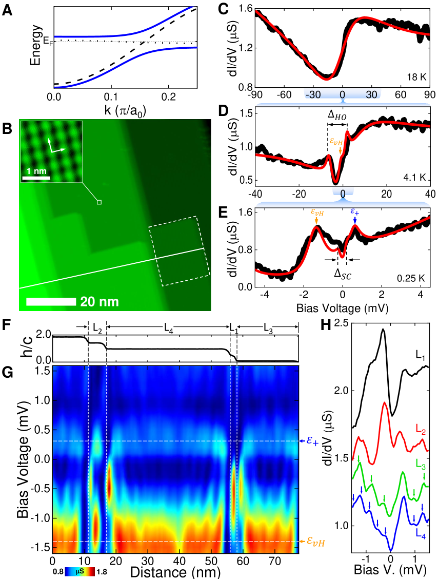
Fig. 1 Tunneling conductance on URu2Si2 terraces. (A) Simplified representation of the low temperature hybridization process leading to heavy fermions. The dashed (dotted) lines show the unhybridized light (heavy) electron bands at high temperatures. Full lines show the resulting low temperature hybridized bands. (B) STM topography image of several terraces on URu2Si2 separated by . Inset shows a zoom into the region at the white square, and unveils the U atomic surface lattice (arrows indicate the in-plane crystalline directions). Dashed rectangle represents the field of view on which we focus in in Fig. 2. (C-E) In black are the tunneling conductance curves at temperatures , and respectively. Red lines are the fits to the model described in the Supplementary Sections S3 and S7. We highlight the size of the gap opening in the HO phase (). (F) Height profile along the white line in (B) identifying four different terraces of sizes to . (G) Tunneling conductance as a function of the bias voltage along the while line in (B). (H) Representative tunneling conductance curves obtained on each terrace. Vertical arrows mark the positions of peaks in and . Orange and blue arrows at and in (D, E, G) identify the van Hove feature inside the HO gap and an additional feature resulting from hybridization in the bandstructure.