Silicon oxynitride platform for linear and nonlinear photonics at NIR wavelengths
Abstract
The development of versatile and novel material platforms for integrated photonics is of prime importance in the perspective of future applications of photonic integrated circuits for quantum information and sensing. Here we present a low-loss material platform based on high-refractive index silicon oxynitride (\ceSiON), which offers significant characteristics for linear and non-linear optics applications in a wide range of red/near-infrared wavelengths. The demonstrated propagation loss dB/cm for visible wavelengths enables the realization of long and intricate circuitry for photon manipulations, as well as the realization of high quality factor resonators. In addition, the proposed \ceSiON shows a high nonlinear coefficient of m2/W, improving the strength of nonlinear effects exploitable for on-chip photon generation schemes.
I Introduction
The development of novel platforms for integrated photonics, characterized by a strong versatility in terms of applications, is of prime importance for the realization of emerging photonics applications in the fields of sensing, metrology, quantum communications and quantum computing Capmany and Pérez (2020); Osgood jr and Meng (2021). Several technologies for photonic integrated circuits (PICs) have been proposed and developed in the last decades. Silicon photonics emerged first, exploiting the advanced CMOS manufacturing techniques optimized for microelectronics. Nowadays, \ceSi photonic devices, based on the Silicon-on-Insulator (SOI) platform, are already spreading in the commercial world, mainly for the telecommunication networks (see Ref. Siew et al. (2021) and references therein). State of the art commercial SOI devices, designed for the telecom C-band, achieve propagation losses of less than dB/cm, offering highly efficient passive components distributed within standard product development kit Bogaerts and Chrostowski (2018); Fahrenkopf et al. (2019); Aalto et al. (2019).
Active components are also implemented within the SOI platform, with phase shifters based on p-n junctions realized directly on the \ceSi waveguides, while for photodetectors and light sources hetero-integration of germanium or III-V compound semiconductor materials is employed. A limiting constrain of \ceSi PICs is that their linear operation is acceptable at wavelengths longer than m (energy bandgap eV) where the core material’s absorption is insignificant, while for nonlinear optical applications excited-carrier (EC) and two-photon absorption (TPA) can still be significant at photon energies .
Silicon Nitride (\ceSiN) has been introduced as an alternative dielectric platform for integrated photonics Blumenthal et al. (2018). It is transparent at wavelengths from nm to m, while very recent developments report on operation in the ultra-violet region Morin et al. (2021). Commercially available platforms show propagation losses dB/cm over the whole operational range, with passive components that show similar performance to their SOI counterparts Moss et al. (2013); Roeloffzen et al. (2018); Liu et al. (2021). Due to its dielectric nature, active components in \ceSiN technology can relay to only relatively slower thermo-optical modulation of the refractive index. Nevertheless, due to the large optical bandgap of eV, \ceSiN does not suffer EC or TPA losses, while nonlinear optical generation can still be significant owing to appreciable third-order nonlinearities. Stoichiometric silicon nitride (\ceSi3N4) offers superior optical quality, however, the film thicknesses should be kept to nm to avoid film cracking due to the large tensile stress. This limitation can be overcome using sophisticated techniques, such as photonic Damascene Pfeiffer et al. (2016) and multilayered TriPleX Heideman et al. (2005); Morichetti et al. (2007); Roeloffzen et al. (2018) processes.
An alternative approach to reduce film stress consists in introducing oxygen into the \ceSiN material, by depositing directly a silicon oxynitride (\ceSiON) film Wörhoff et al. (1999); Germann et al. (2000); Samusenko et al. (2016); Chen et al. (2017). The refractive index of \ceSiON can be continuously tuned between 1.45 (\ceSiO2) and 2.00 (\ceSi3N4) by controlling the relative content of \ceO and \ceN in the film. The material loss can be lower than that of \ceSiN, meantime maintaining a very low stress for film thicknesses of up to few micrometers. As a drawback, the reduction of the material refractive index causes an increase in the device footprint, as well as a weakening of the thermo-optical and nonlinear optical characteristics of the guiding components Trenti et al. (2018).
In this work, we present a novel, low-loss, photonic platform based on \ceSiON channel waveguides, capable to manage a wide range of VIS/NIR wavelengths for both linear and nonlinear optics applications. The core material consists in a relatively high refractive index \ceSiON (1.66 at 850nm wavelength), which enables small footprint PIC designs with propagation losses dB/cm, improvable by at least a factor of two. The material shows an optical bandgap of 3.8 eV with a relatively strong optical nonlinearity of m2/W close to the TPA absorption edge. This, combined with the possibility to remove locally the cladding without damaging the waveguide, offers large versatility to engineer the waveguide dispersion for applications such as nonlinear Four-Wave Mixing (FWM) in ring resonator devices. Our \ceSiON platform has the potential to be further developed for the monolithic integration of all necessary functionalities – photon sources, light manipulation circuits and photon detection (recently proven in Ref. Bernard et al. (2021)) – on a single chip, operating at room temperature, for classical and quantum applications.
The paper is structured as follows: Sec. II presents the technological approach, Sec. III and IV describe the linear and nonlinear properties of the \ceSiON platform, respectively. In Sec. V we describe the dispersion engineering of ring resonators for non-linear FWM and the fabrication of these devices. Finally, in Sec. VI we summarize our results and draw conclusions.
II Photonic platform
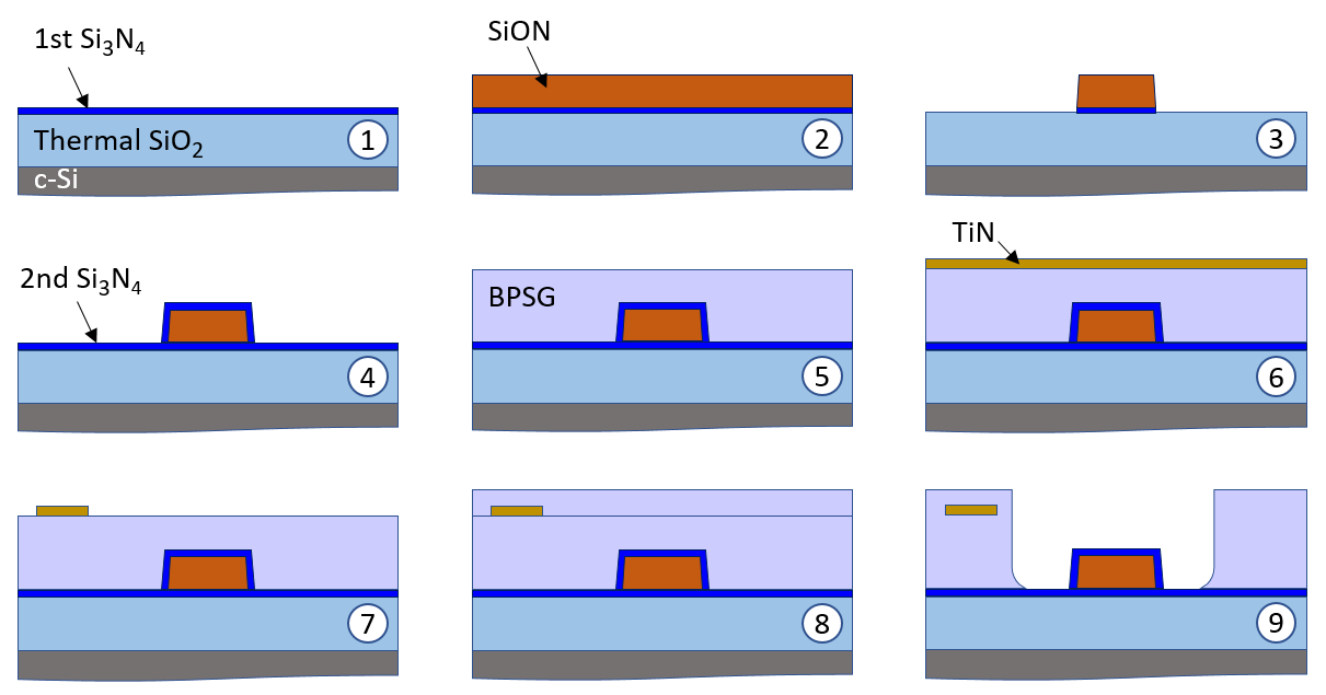
The photonic platform we introduce is based on the use of high-index \ceSiON for the core material and \ceSiO2 claddings, resulting in a relatively large core/cladding index contrast of . In addition, the channel waveguide is encapsulated between two thin films of \ceSi3N4. These last act as an etch-stop barrier during the wet chemical etching, which is used to open windows in the waveguide’s top \ceSiO2 cladding in specific locations on the chip, without the risk to underetch the bottom \ceSiO2 cladding. The removal of top \ceSiO2 is an optional process, which can be used for different purposes, for example, a chemical functionalization of the waveguide surface for sensing applications Densmore et al. (2009); Washburn et al. (2009); Mukundan et al. (2009); Heideman et al. (2012); Samusenko et al. (2016) or, as it will be discussed in Section V, in cases when the refractive index dispersion of waveguides should be engineered for non-linear optics applications Turner et al. (2006); Mas et al. (2010); Zhao et al. (2015); Zhang et al. (2018); Guo et al. (2018); Zhao et al. (2020).
The fabrication process of the proposed platform is schematically described in Fig. 1. Starting from a 6 inch silicon wafer, first a m silicon oxide has been grown by wet thermal oxidation at C to form the bottom cladding. On top of it, a nm thick \ceSi3N4 is deposited in a Low-pressure chemical vapor deposition (LPCVD) furnace at C, followed by a nm \ceSiON film deposition in a plasma-enhanced chemical vapor deposition (PECVD) chamber using \ceSiH4, \ceN2O and \ceNH3 gas precursors. Next, the photonic devices were defined by photoresist patterning using an i-line stepper lithography, and the pattern transferred to the \ceSiON/\ceSi3N4 layers using reactive ion etching (RIE). Then, the \ceSiON waveguides were thermally treated at C for 90 min in a \ceN2 atmosphere to allow the release of residual \ceH2 and the improvement of the optical properties of the \ceSiON film. Next, a second deposition of nm \ceSi3N4 was performed, followed by a deposition of LPCVD borophosphosilicate glass (\ceBPSG) and PECVD \ceSiO2 films at C and C, respectively, to form the top cladding of a total of m.
In a next step, a multi-stack of 150 nm \ceTiN and 1200 nm of \ceAl was sputtered, patterned, and etched with RIE to allow for the realization of metal lines, contact pads and micro-heaters for the thermo-optical tuning of photonic components. The top \ceAl film was selectively removed on top of the micro-heaters via wet chemical etching in order to realize efficient \ceTiN micro-resistances with a sheet resistance of /sq. The wafer was covered with 500 nm PECVD \ceSiO2 protective film, which was then removed from pad positions to allow for external electrical contact.
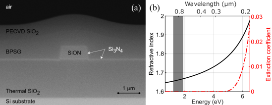
Finally, the chip boundaries and the waveguide facets were defined by RIE of the dielectric multilayer, with an additional m deep etch into the \ceSi substrate through a Bosch process in order to ease the butt-coupling between optical fibers and waveguides. Figure 2a shows the SEM cross-sectional micrograph of the core of an nm \ceSiON waveguide. All the different films, including the surrounding nm-thick \ceSi3N4 film, the bottom and top claddings as well as the \ceSi substrate are clearly visible.
III Linear properties
III.1 Material dispersion
The optical properties of the \ceSiON films were characterized by variable-angle spectroscopic ellipsometry (VASE). The refractive index was modeled with the New Amorphous model based on the Forouhi-Bloomer dispersion equations Forouhi and Bloomer (1988)
| (1) |
where is the refractive index when , and contain the material characteristics
| (2) | ||||
| (3) |
This model allows to estimate the optical band gap of the platform’s core material. The parameters , and describe, respectively, the amplitude, the spectral width and the spectral position of the absorption peak in energy units. The obtained dispersions for the real refractive index and the extinction coefficient are plotted in Fig. 2b.
Of particular interest for this work, the refractive index of \ceSiON has been engineered to be higher than that of typical low-index \ceSiON used in previous works Wörhoff et al. (1999); Bona et al. (2003); Chen et al. (2019). This choice allows to design optical components with smaller footprint and larger optical mode confinement. Despite the relatively higher refractive index (1.66 at 850 nm), the estimated band-gap of eV allows the photonic platform to be used without material absorption loss in the whole near-infrared and visible regions.
III.2 Propagation loss
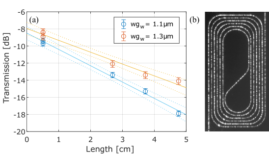
Another important property to be optimized for a photonic platform is the propagation loss of waveguides, that can be attributed to several sources such as: the material absorption, the radiative loss at bends, the loss toward the silicon substrate and the scattering due to surface roughness. The overall value of propagation loss, per unit length, can be characterized emulating the cutback method, by measuring the input/output power ratio of spiral-like waveguides of different lengths, as shown in Fig. 3.
This characterization was realized for two different widths of waveguides, namely m and m, resulting in average losses of, respectively, dB/cm and dB/cm in the studied wavelength region 740 nm to 840 nm, with a coupling loss of dB per facet. Note that, at the moment of writing this manuscript, an improvement of our etching technique has lead to propagation losses of the same \ceSiON waveguides as low as 0.8 dB/cm.
IV Non-linear properties
The third-order optical nonlinearities of the \ceSiON photonic platform have been studied by exploiting the phenomenon of Self-Phase-Modulation (SPM) Stolen and Lin (1978); Tzoar and Jain (1981). An intense laser pulse, which propagates in a nonlinear medium, induces a local variation of the refractive index due to strong light-matter interactions. This variation causes a phase shift between the spectral components of the pulse resulting in a modulation of pulse spectrum. Consequently, by measuring the spectral broadening of an ultra-short pulse with known power, one can retrieve the non-linear index of refraction of the material. In particular, following the split-step method described in Ref. Agrawal (2000), one can simulate the expected SPM effect for a given set of parameters, including: the material’s coefficient, the waveguide geometry and the initial characteristics of the pulse. Then, by comparing the simulated results with the measured SPM spectra, the nonlinear coefficient of the material can be estimated.
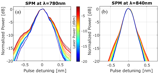
The SPM measurements were obtained using a mode-locked Ti:Sapphire laser, tunable in the wavelength range 720 nm-840 nm, with a -dB pulse-width of nm (2 ps) and a repetition rate of 82 MHz. The laser is directly injected into the \ceSiON waveguide using a lensed glass optical fiber. The transmitted pulse is collected with a second identical fiber at the waveguide output and analyzed in an Optical Spectrum Analyzer with nm spectral resolution and sensitivity of -60 dBm.
The pulse-broadening experiment was performed for different input powers, ranging from 0 dBm to -20 dBm measured at the output of the waveguide, in order to verify the intensity dependence of SPM. Considering that the non-linear effects on the input pulse may occur also in the injection optics, composed of lenses and fibers, it is important to attenuate the power injected into the waveguides after the external optics. Therefore, the variation of the power coupled to the waveguide was realized by moving the input-fiber away from the waveguide’s facet, to decrease the coupling efficiency. Figure 4 shows an example of the experimental data, obtained for two different pulses with central wavelengths at nm and nm.
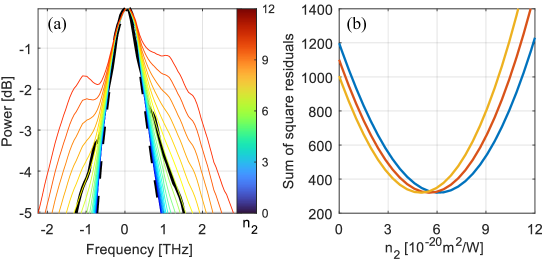
In order to estimate the unknown Kerr nonlinearity of the \ceSiON material, we have performed numerical simulations which transform an input pulse spectrum into a broadened one. Having the knowledge of the waveguide’s length and propagation loss, of the effective mode area (obtained by numerical simulations) and of the effective refractive index, the nonlinear Kerr coefficient can be then estimated according to the following procedure. For each set of measurements, the lowest-power signal is taken as the reference input pulse-shape. Then, for each power, a set of expected output signals are simulated with the split-step method for different values of (Fig. 5a). The final value of is thus estimated as the one that minimizes the spectral difference between the experimental data and the numerical solution (Fig. 5b). The main source of error in the estimation of within this approach is given by the error of the propagation loss imposed in the numerical model. The uncertainty of the estimated was evaluated by simulating the spectra at three values of propagation loss: , and , and taking the difference as the estimated error of .
| waveguide | width | length | (780 nm) | (840 nm) |
|---|---|---|---|---|
| wg A | m | mm | ||
| wg B | m | mm | ||
| wg C | m | mm | ||
| wg D | m | mm |
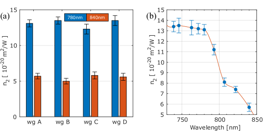
The described numerical SPM simulations method is based on the experimental inputs, which account for the geometrical dimensions and linear optical properties of the fabricated waveguides. In order to verify the robustness of our approach, we applied this method to study a set of four waveguides. In particular, a pair of waveguides was studied for two different nominal widths of 1100 nm and 1300 nm, as described in Table 1. The validation test, reported in Fig. 6a, shows that at a fixed wavelength the estimations of are independent on the waveguide’s geometry, within error, and therefore confirms the reliability of our analysis. The results are also consistent with previous works Trenti et al. (2018); Ikeda et al. (2008); Sheik-Bahae et al. (1990), indicating that the values of our \ceSiON material are in between the expected values for pure \ceSiO2 and pure \ceSi3N4.
In the following, we have selected one of the 1100 nm wide waveguides (sample A) and performed a spectral analysis of the variation of with wavelength. Figure 6b shows that the Kerr coefficient strongly increases while reducing the pump wavelength from Near-Infrared to Visible-Red region. This behavior is in accordance with the theoretical model that foresees a maximum in the nonlinear coefficient located close to the TPA edge at Sheik-Bahae et al. (1990), corresponding to a wavelength of about nm for our \ceSiON platform.
V Dispersion-engineered \ceSiON ring resonators for generation of correlated photon pairs
The knowledge of the linear and non-linear properties of the developed \ceSiON photonic platform makes it possible to engineer the modal refractive index, , of the waveguide to match particular applications. Nonlinear schemes of generation of non-classical states of NIR photons often relay on SiN integrated microphotonic devices Zhao et al. (2015); Cernansky et al. (2018); Lu et al. (2019); Zhao et al. (2020). In this section, we describe our approach for the engineering and realization of \ceSiON-based ring resonator devices for on-chip generation of entangled photon pairs via Spontaneous Four Wave Mixing (SFWM).
The dependence of on the light angular frequency leads to the dispersive nature of the mode’s propagation constant , which can be expressed as a Taylor series around a central frequency
| (4) |
where the diverse orders account for different propagation phenomena. In particular, for nonlinear wave interactions, the first two orders and play an important role and represent, respectively, the group index and the Group Velocity dispersion (GVD):
| (5a) | |||
| (5b) | |||
In a ring resonator, the group velocity defines the spectral separation between successive resonant modes – the free-spectral range (FSR) – following the relation , where is the physical length of the cavity. A flat dispersion of over a range of frequencies provides energy-equidistant cavity resonances, which is essential to fulfill the energy conservation requirement, for example, in nonlinear FWM and frequency comb generation experiments Cernansky et al. (2018); Zhao et al. (2020), where the pump, the signal and the idler should satisfy the relation .
The parameter describes how the different spectral components of a propagating pulse travel, and in either case (normal dispersion) or (anomalous dispersion) result in temporal broadening of the pulse. The case of at some frequency – the zero dispersion frequency (ZDF) – is of particular interest for nonlinear optical applications because around the ZDF different spectral components experience largely reduced second-order dispersion. In SFWM experiments with microring resonators around ZDF the spectral spread of is minimal and the flatness of provides with larger nonlinear generation bandwidth Agha et al. (2009); Agrawal (2000).
We performed numerical axisymmetric simulations based on the Finite Elements Method in order to develop proper geometries for a device operating at NIR wavelengths, supporting single-mode characteristics and showing an anomalous GVD over the spectral range of interest. The radius of the studied ring resonators was set to 25 m. This choice is motivated by the necessity to keep the ring radius large enough to avoid radiative losses but small enough to provide with nm in order to minimize the spectral overlap of pump pulses with more than one mode around 800 nm of wavelength.
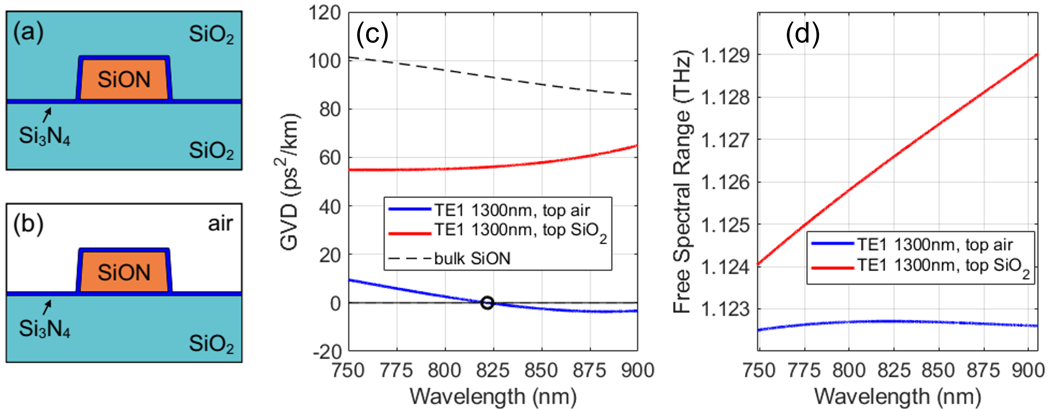
We first investigated a conventional geometry, in which the waveguide of a slightly trapezoidal form is fully embedded within the SiO2 cladding (Fig. 7a). The lateral boundaries of the waveguide have an inclination angle of , which is the typical value according to our fabrication process. The height of the \ceSiON waveguide was fixed to 500 nm. Simulations were performed by varying the ring waveguide width from 900 nm to 1700 nm and the azimuthal number of the fundamental radial mode from 270 to 330, covering a wavelength span of 200 nm around nm. The obtained results for both the quasi transverse electric (TE) and magnetic (TM) modes showed that the GVD remains normal for all ring widths within the spectral range between 750 nm and 950 nm.
Next, we performed simulations of the same ring geometry substituting the top SiO2 cladding with air (Fig. 7b). This new configuration turned to be particularly interesting since the GVD appeared to be much more sensitive to the variations of the waveguide width. We found that the GVDs of air-cladded resonators are already anomalous for smaller widths ( nm) and turn slowly into a normal one over 1350 nm. In Fig. 7c we compare the calculated GVDs for 1300 nm waveguide width rings in both configurations with top SiO2 (red) and air-claddings (blue). A zero-dispersion point is observed at around nm for a 1300 nm waveguide width rings. The air-cladded ring shows sufficiently flat dispersion of the group index and, consequently, a stable FSR over a large span of wavelengths from 800 to 850 nm’s (Fig. 7d). The effective nonlinearity for the m2 ring at the zero-dispersion point of 822 nm is estimated to be of the order of 1 m-1W-1.
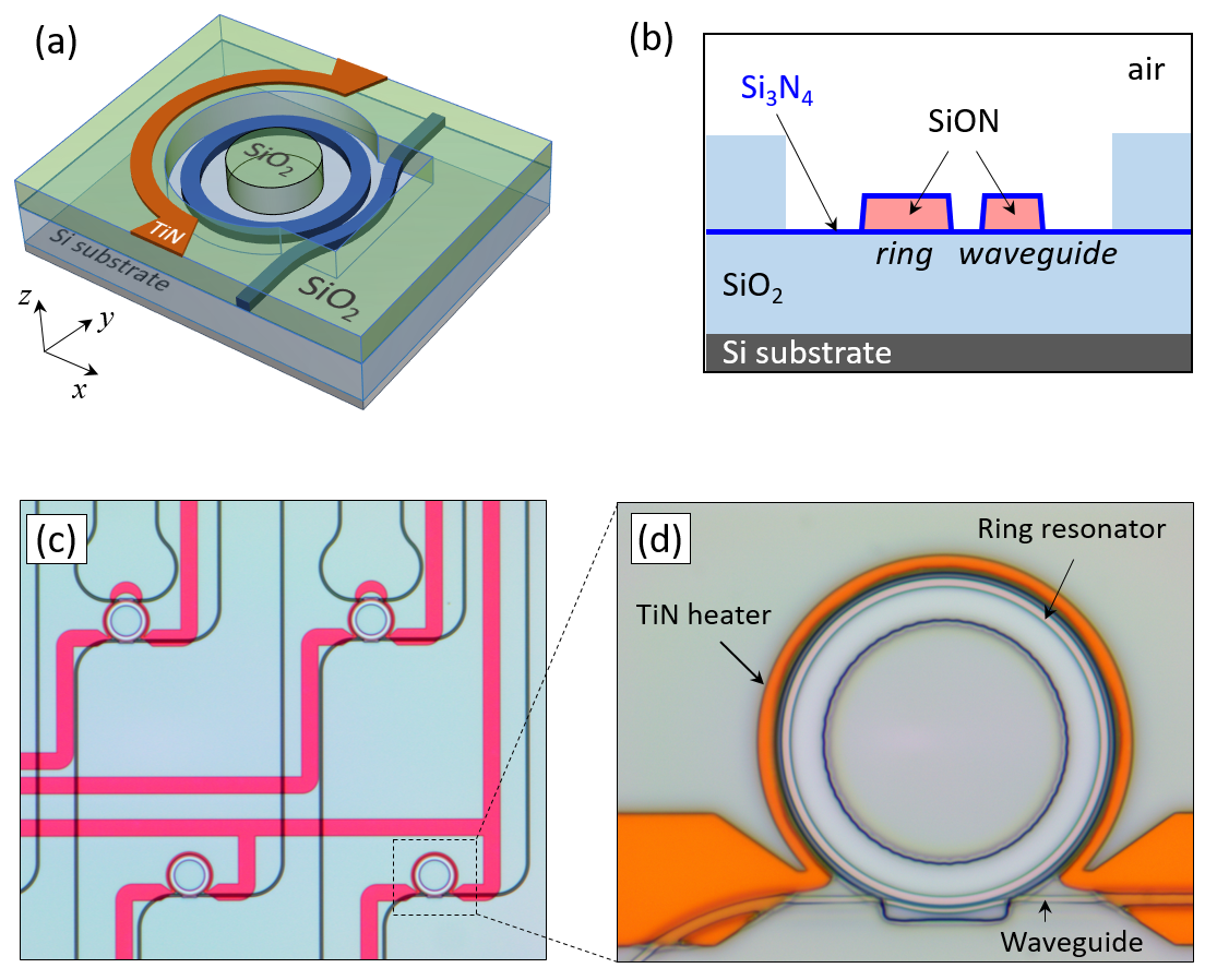
A schematic of the dispersion-engineered resonator, which has been fabricated on the same chip together with spiral waveguides, is shown in Fig. 8a. The top SiO2 cladding around the resonators was removed via a selective wet-etching procedure in buffered HF solution during which the 50 nm Si3N4 film acts as an ideal etch-stop film to prevent underetching of waveguiding components. The opening window around the ring was designed such that the remaining top SiO2 cladding after wet etching is retracted to a safe distance of at least m from the waveguide (Fig. 8b). Figure 8c shows an optical micrograph of arrays of ring resonators both in add-drop and all-pass configurations, while a blowup around an air-cladded all-pass ring resonator is shown in Fig. 8d. The linear characterization and non-linear sFWM experiments on these devices are currently ongoing, however, their discussion is out of the scope of the current manuscript.
VI Conclusions
In this work, we have demonstrated a new silicon oxynitride-based integrated photonic platform for linear and nonlinear application in the VIS-NIR wavelength range. The fabricated devices show a low propagation loss dB/cm, comparable to commercially available devices at nm wavelength and with ongoing improvement of at least a factor two. We have demonstrated that, despite the reduction of the refractive index with respect to \ceSiN, the \ceSiON waveguides preserve a relatively strong optical nonlinearity of m2/W around the wavelength nm. Furthermore, thanks to the possibility to remove locally the cladding without damaging the waveguide, our platform allows for a larger versatility in engineering the waveguide dispersion. This enables to investigate one of the specific and peculiar applications of nonlinear FWM by properly adjusting the group index and group velocity dispersion in order to enhance nonlinear photon pair generation in ring resonators. By combining the good linear properties, the promising optical nonlinearities for on-chip photon generation and our recently developed technology for on-chip photon detection Bernard et al. (2021), we envision the potential of this platform to achieve, in the near future, a full integration of photon generation sources, manipulation and detection on a single Silicon chip, operating at room temperature, for classical and quantum photonics applications.
VII Acknowledgment
Funding. European Commission (777222, 899368).
Acknowledgments.
The authors are thankful to M. Bernard and G. Pucker for the fruitful discussions regarding the design and fabrication of the photonic devices.
Disclosures.
The authors declare no conflicts of interest.
Data availability. Data underlying the results presented in this paper are not publicly available at this time but may be obtained from the authors upon reasonable request.
References
- Capmany and Pérez (2020) J. Capmany and D. Pérez, Programmable Integrated Photonics (Oxford University Press, 2020).
- Osgood jr and Meng (2021) R. Osgood jr and X. Meng, Principles of Photonic Integrated Circuits: Materials, Device Physics, Guided Wave Design (Springer Nature, 2021).
- Siew et al. (2021) S. Y. Siew, B. Li, F. Gao, H. Y. Zheng, W. Zhang, P. Guo, S. W. Xie, A. Song, B. Dong, L. W. Luo, et al., Journal of Lightwave Technology 39, 4374 (2021).
- Bogaerts and Chrostowski (2018) W. Bogaerts and L. Chrostowski, Laser & Photonics Reviews 12, 1700237 (2018).
- Fahrenkopf et al. (2019) N. M. Fahrenkopf, C. McDonough, G. L. Leake, Z. Su, E. Timurdogan, and D. D. Coolbaugh, IEEE Journal of Selected Topics in Quantum Electronics 25, 1 (2019).
- Aalto et al. (2019) T. Aalto, M. Cherchi, M. Harjanne, S. Bhat, P. Heimala, F. Sun, M. Kapulainen, T. Hassinen, and T. Vehmas, IEEE Journal of selected topics in quantum electronics 25, 1 (2019).
- Blumenthal et al. (2018) D. J. Blumenthal, R. Heideman, D. Geuzebroek, A. Leinse, and C. Roeloffzen, Proceedings of the IEEE 106, 2209 (2018).
- Morin et al. (2021) T. J. Morin, L. Chang, W. Jin, C. Li, J. Guo, H. Park, M. A. Tran, T. Komljenovic, and J. E. Bowers, Optica 8, 755 (2021).
- Moss et al. (2013) D. J. Moss, R. Morandotti, A. L. Gaeta, and M. Lipson, Nature photonics 7, 597 (2013).
- Roeloffzen et al. (2018) C. G. Roeloffzen, M. Hoekman, E. J. Klein, L. S. Wevers, R. B. Timens, D. Marchenko, D. Geskus, R. Dekker, A. Alippi, R. Grootjans, et al., IEEE journal of selected topics in quantum electronics 24, 1 (2018).
- Liu et al. (2021) J. Liu, G. Huang, R. N. Wang, J. He, A. S. Raja, T. Liu, N. J. Engelsen, and T. J. Kippenberg, Nature communications 12, 1 (2021).
- Pfeiffer et al. (2016) M. H. Pfeiffer, A. Kordts, V. Brasch, M. Zervas, M. Geiselmann, J. D. Jost, and T. J. Kippenberg, Optica 3, 20 (2016).
- Heideman et al. (2005) R. Heideman, A. Melloni, M. Hoekman, A. Borreman, A. Leinse, and F. Morichetti, in Proc. of the 9th IEEE/LEOS Symp. in the Benelux (2005) pp. 71–74.
- Morichetti et al. (2007) F. Morichetti, A. Melloni, M. Martinelli, R. G. Heideman, A. Leinse, D. H. Geuzebroek, and A. Borreman, Journal of Lightwave technology 25, 2579 (2007).
- Wörhoff et al. (1999) K. Wörhoff, A. Driessen, P. Lambeck, L. Hilderink, P. W. Linders, and T. J. Popma, Sensors and Actuators A: Physical 74, 9 (1999).
- Germann et al. (2000) R. Germann, H. Salemink, R. Beyeler, G. Bona, F. Horst, I. Massarek, and B. Offrein, Journal of the Electrochemical Society 147, 2237 (2000).
- Samusenko et al. (2016) A. Samusenko, D. Gandolfi, G. Pucker, T. Chalyan, R. Guider, M. Ghulinyan, and L. Pavesi, Journal of lightwave technology 34, 969 (2016).
- Chen et al. (2017) D. Chen, A. Kovach, X. Shen, S. Poust, and A. M. Armani, ACS Photonics 4, 2376 (2017).
- Trenti et al. (2018) A. Trenti, M. Borghi, S. Biasi, M. Ghulinyan, F. Ramiro-Manzano, G. Pucker, and L. Pavesi, AIP Advances 8, 025311 (2018).
- Bernard et al. (2021) M. Bernard, F. Acerbi, G. Paternoster, G. Piccoli, L. Gemma, D. Brunelli, A. Gola, G. Pucker, L. Pancheri, and M. Ghulinyan, Optica 8, 1363 (2021).
- Densmore et al. (2009) A. Densmore, M. Vachon, D.-X. Xu, S. Janz, R. Ma, Y.-H. Li, G. Lopinski, A. Delâge, J. Lapointe, C. Luebbert, et al., Optics letters 34, 3598 (2009).
- Washburn et al. (2009) A. L. Washburn, L. C. Gunn, and R. C. Bailey, Analytical chemistry 81, 9499 (2009).
- Mukundan et al. (2009) H. Mukundan, A. S. Anderson, W. K. Grace, K. M. Grace, N. Hartman, J. S. Martinez, and B. I. Swanson, Sensors 9, 5783 (2009).
- Heideman et al. (2012) R. Heideman, M. Hoekman, and E. Schreuder, IEEE Journal of Selected topics in quantum electronics 18, 1583 (2012).
- Turner et al. (2006) A. C. Turner, C. Manolatou, B. S. Schmidt, M. Lipson, M. A. Foster, J. E. Sharping, and A. L. Gaeta, Optics express 14, 4357 (2006).
- Mas et al. (2010) S. Mas, J. Caraquitena, J. V. Galán, P. Sanchis, and J. Martí, Optics express 18, 20839 (2010).
- Zhao et al. (2015) H. Zhao, B. Kuyken, S. Clemmen, F. Leo, A. Subramanian, A. Dhakal, P. Helin, S. Severi, E. Brainis, G. Roelkens, et al., Optics letters 40, 2177 (2015).
- Zhang et al. (2018) Y. Zhang, J. Zou, and J.-J. He, Optics Express 26, 26057 (2018).
- Guo et al. (2018) K. Guo, J. B. Christensen, X. Shi, E. N. Christensen, L. Lin, Y. Ding, H. Ou, and K. Rottwitt, IEEE Photonics Journal 10, 1 (2018).
- Zhao et al. (2020) Y. Zhao, X. Ji, B. Y. Kim, P. S. Donvalkar, J. K. Jang, C. Joshi, M. Yu, C. Joshi, R. R. Domeneguetti, F. A. Barbosa, et al., Optica 7, 135 (2020).
- Forouhi and Bloomer (1988) A. Forouhi and I. Bloomer, Physical review B 38, 1865 (1988).
- Bona et al. (2003) G.-L. Bona, R. Germann, and B. J. Offrein, IBM Journal of Research and Development 47, 239 (2003).
- Chen et al. (2019) D. Chen, A. Kovach, S. Poust, V. Gambin, and A. M. Armani, Applied Physics Letters 115, 051105 (2019).
- Stolen and Lin (1978) R. H. Stolen and C. Lin, Physical Review A 17, 1448 (1978).
- Tzoar and Jain (1981) N. Tzoar and M. Jain, Physical Review A 23, 1266 (1981).
- Agrawal (2000) G. P. Agrawal, in Nonlinear Science at the Dawn of the 21st Century (Springer, 2000) pp. 195–211.
- Ikeda et al. (2008) K. Ikeda, R. E. Saperstein, N. Alic, and Y. Fainman, Optics express 16, 12987 (2008).
- Sheik-Bahae et al. (1990) M. Sheik-Bahae, D. J. Hagan, and E. W. Van Stryland, Physical review letters 65, 96 (1990).
- Cernansky et al. (2018) R. Cernansky, F. Martini, and A. Politi, Optics Letters 43, 855 (2018).
- Lu et al. (2019) X. Lu, Q. Li, D. A. Westly, G. Moille, A. Singh, V. Anant, and K. Srinivasan, Nature physics 15, 373 (2019).
- Agha et al. (2009) I. H. Agha, Y. Okawachi, and A. L. Gaeta, Optics Express 17, 16209 (2009).