Piezoelectric quantum spin Hall insulator VCClBr monolayer with pure out-of-plane piezoelectric response
Abstract
The combination of piezoelectricity with nontrivial topological insulating phase in two-dimensional (2D) systems, namely piezoelectric quantum spin Hall insulator (PQSHI), is intriguing for exploring novel topological states toward the development of high-speed and dissipationless electronic devices. In this work, we predict a PQSHI Janus monolayer VCClBr constructed from , which is dynamically, mechanically and thermally stable. In the absence of spin orbital coupling (SOC), VCClBr is a narrow gap semiconductor with gap value of 57 meV, which is different from Dirac semimetal . The gap of VCClBr is due to built-in electric field caused by asymmetrical upper and lower atomic layers, which is further confirmed by external-electric-field induced gap in . When including SOC, the gap of VCClBr is improved to 76 meV, which is larger than the thermal energy of room temperature (25 meV). The VCClBr is a 2D topological insulator (TI), which is confirmed by topological invariant and nontrivial one-dimensional edge states. It is proved that the nontrivial topological properties of VCClBr are robust against strain (biaxial and uniaxial cases) and external electric field. Due to broken horizontal mirror symmetry, only out-of-plane piezoelectric response can be observed, when biaxial or uniaxial in-plane strain is applied. The predicted piezoelectric strain coefficients and are -0.425 pm/V and -0.219 pm/V, which are higher than or compared with ones of many 2D materials. Finally, another two Janus monolayer VCFBr and VCFCl (dynamically unstable) are constructed, and they are still PQSHIs. Moreover, their and are higher than ones of VCClBr, and the (absolute value) of VCFBr is larger than one. According to out-of-plane piezoelectric coefficients of VCXY (XY=F, Cl and Br), (X=F, Cl and Br; Y=I) and NiXY (XY=Cl, Br and I), it is concluded that the size of out-of-plane piezoelectric coefficient has a positive relation with electronegativity difference of X and Y atoms. Our works enrich the diversity of Janus 2D materials, and open a new avenue in searching for PQSHI with large out-of-plane piezoelectric response, which provides a potential platform in nanoelectronics.
I Introduction
The discovery of 2D materials has spurred a surge of experimental and theoretical interests in understanding their physical and chemical properties. The piezoelectricity of 2D materials has been a research hotspot in the ever-increasing energy conversion areaq4 ; q4-1 , which requires a 2D system to be non-centrosymmetrical. The 2H- is a typical 2D piezoelectric material, which has been confirmed experimentallyq5 . In theory, piezoelectric properties of many 2D materials have been reportedq11 ; q7 ; q10 ; q9 ; q13 ; q17 ; q16 . Strong in-plane piezoelectric response is common, while large out-of-plane piezoelectric strain coefficient is rare. Searching for 2D materials with large out-of-plane piezoelectric response has become an important quest due to its compatibility with bottom/top gate technologies. Another interesting feature of 2D systems is nontrivial topology, and TI of them is also called as quantum spin Hall insulator (QSHI) with spin-momentum-locked conducting edge states. The first QSHI is predicted in graphenet3 , and then the HgTe/CdTe and InAs/GaSb quantum wells are experimentally confirmed as QSHIs t4 ; t5 . Theoretically, many 2D systems have been proposed as QSHIs by first-principle calculationst6 ; t7 ; qt3 ; t8 ; t9 ; t10 . Searching for QSHI with large gap (larger than 25 meV) is very important for room temperature device applications.
Multifunctional 2D materials are of particular interest due to providing a potential platform for multi-functional electronic devices. Compared to individual piezoelectricity or nontrivial band topology in a single 2D material, their combination can provide a unique opportunity for intriguing physics and practical device applications. To search PQSHI, there are two ways :(1) seeking for nontrivial band topology from 2D piezoelectric materials; (2) finding or constructing non-centrosymmetrical QSHI, which may be a executable method, especially for sandwich structure. It is well known that a sandwich structure can be used as a parent to construct Janus structure, which lacks central symmetry, giving rise to piezoelectric effectgsd1 ; gsd2 ; gsd4 . The typical Janus MoSSe monolayer has been experimentally synthesized based on with symmetrical upper and lower atomic layerse1 ; e2 . However, the nontrivial topology may be broken by building Janus structure from a QSHIgsd4 ; gsd4-1 . The Janus and MoSSe as derivatives of QSHI and 1T’- lose nontrivial topology. However, strain can make them possess topological properties of their parentsgsd4 ; gsd4-1 .
Recently, based on VOCl as a prototype, 20 2D monolayers VXY (X = B, C, N, O and F; Y = F, Cl, Br and I) are predicted by means of first-principles calculationsw-1 . They possess emerging topological, magnetic and dielectric properties, which depend electron occupation, ligand electronegativity and crystal field strength. Calculated results demonstrate that the VCY systems exhibit nontrivial topological propertiesw-1 . Their crystal structure possesses central symmetry, which leads to disappeared piezoelectricity. However, this structure can be regarded as a sandwich structure. These provide a possibility to induce PQSHI by constructing Janus structure based on VCY monolayer as parent.
In this work, we build a Janus crystal structure VCClBr, which can be attained by replacing the top Cl layer in monolayer with Br atoms. Calculated results show that VCClBr indeed is a PQSHI with dynamical, mechanical and thermal stabilities. It is proved that nontrivial band topology of VCClBr is robust against strain and external electric field. The calculated out-of-plane piezoelectric response is strong compared with ones of many 2D materialsq7 ; q9 , like Janus transition metal dichalcogenide (TMD) monolayers. Finally, by analysing out-of-plane piezoelectric coefficients of VCXY (XY=F, Cl and Br), (X=F, Cl and Br; Y=I)w-2 and NiXY (XY=Cl, Br and I)w-3 , the strong out-of-plane piezoelectric response can be attained by constructing Janus monolayer with large electronegativity difference of X and Y atoms. Our works highlight multifunctionalities of Janus VCClBr, which is promising for applications in the next-generation topotronic and piezoelectric devices.
The rest of the paper is organized as follows. In the next section, we shall give our computational details. In the next few sections, the crystal structure and stability, electronic structures and piezoelectric properties of Janus monolayer VCClBr are shown. Finally, our discussion and conclusions are given.
| Name | Dynamics | |||||
|---|---|---|---|---|---|---|
| VCClBr | 3.257 | 3.959 | 76 | D | 1 | Y |
| VCFBr | 3.140 | 3.949 | 45 | I | 1 | N |
| VCFCl | 3.092 | 3.949 | 20 | D | 1 | N |
II Computational detail
We perform density functional theory (DFT) calculations1 using the Vienna Ab initio Simulation Package (VASP), with projected augmented wave methodpv1 ; pv2 ; pv3 . The total energy convergence criterion and cutoff energy for plane-wave expansion are set to eV and 500 eV, respectively. The exchange-correlation potential is adopted within generalized gradient approximation (GGA) of Perdew, Burke and Ernzerhofpbe . Furthermore, Heyd-Scuseria-Ernzerhof screened hybrid functional (HSE06)hse is also employed to confirm nontrivial topology. The SOC is included to investigate electronic structures and topological properties of VCClBr. To sample the Brillouin zone (BZ), a Monkhorst-Pack mesh of 16131 is adopted for geometry optimization, and the residual force on each atom is required to be less than 0.0001 . To eliminate spurious interactions with its periodic images, a vacuum region of more than 18 is adopted in the direction perpendicular to the VCClBr monolayer.
The phonon dispersion spectrums are attained by finite displacement method with a supercell of 551, as implemented in Phonopy codepv5 . To calculate the second order interatomic force constants (IFCs), a 221 k-mesh is employed with kinetic energy cutoff of 500 eV. The elastic stiffness tensor and piezoelectric stress coefficients are attained by using strain-stress relationship (SSR) and density functional perturbation theory (DFPT) methodpv6 , respectively. The 2D elastic coefficients and piezoelectric stress coefficients have been renormalized by the the length of unit cell along direction (): = and =. A 16131 Monkhorst-Pack mesh is adopted to calculate and by using GGA. WannierTools codew1 is used to calculate surface state and topological invariant, based on the tight-binding Hamiltonians constructed from maximally localized Wannier functions by employing -orbitals of V atoms and -orbitals of C, Cl and Br atoms, as implemented in Wannier90 codew2
III Crystal structure and stability
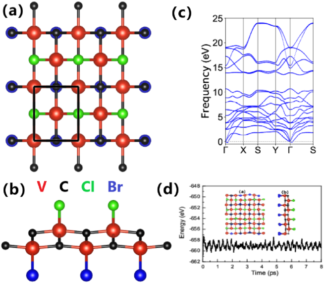
As shown in Figure 1 (a) and (b), the middle VC layer of VCClBr is sandwiched by Cl and Br layers, which can be considered as a Janus structure. The VCClBr can be constructed by replacing top Cl atom layer in monolayer with Br atoms. Its each V atom is 6- fold coordinated with four C , one Cl and one Br atoms, giving rise to a strongly distorted octahedron unit. The symmetry of VCClBr (No.25) is lower than that of (No.59) due to the lack of horizontal mirror symmetry. Namely, the has centrosymmetry with disappeared piezoelectricity, while the VCClBr lacks inversion symmetry, possessing piezoelectricity. The optimized lattice constant of VCClBr is a=3.257 and b=3.959 . Due to different atomic sizes and electronegativities of Cl and Br atoms, inequivalent bond lengths can be observed, for example =2.449 and =2.575 , which can induce an electrostatic potential gradient, giving rise to a built-in electric field.
To validate its dynamic stability, the phonon dispersions of VCClBr are calculated, which is plotted in Figure 1 (c). No imaginary vibrational frequency with three acoustic and fifteen optical phonon branches is observed, suggesting that VCClBr is dynamically stable. In addition, by performing ab-initio molecular dynamics (AIMD) simulations, the thermal stability of VCClBr with a supercell of 441 for more than 8000 fs at 300 K is examined. The total energy fluctuations as a function of simulation time along with the final configurations are plotted in Figure 1 (d). Calculated results show that VCClBr undergoes no structural reconstruction with small energy fluctuates, indicating its thermal stability.
To further check the mechanical stability of VCClBr, its elastic constants are calculated. By using Voigt notation, the elastic tensor with point-group symmetry can be written as:
| (1) |
The calculated =130.67 , =215.81 , =17.08 and =53.45 . The calculated elastic constants satisfy the Born criteria of mechanical stability:
| (2) |
Therefore, VCClBr is mechanically stable.
Since the and of VCClBr are very different, the anisotropy of its Young’s moduli and Poisson’s ratios should be very distinct. The direction-dependent and can be attained by the following two formulasela ; ela1 :
| (3) |
| (4) |
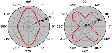
where the is the angle of direction with / direction defined as as /, , and . As plotted in Figure 2, the and of VCClBr show very strong anisotropy. The is 129.32/213.58 along / direction, and 0.079/0.131 for .
IV Electronic structures
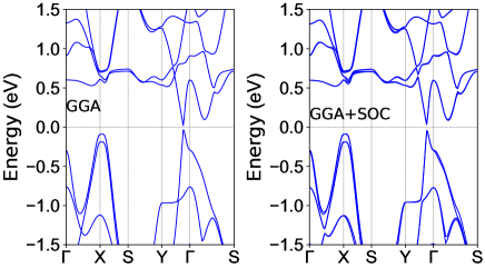
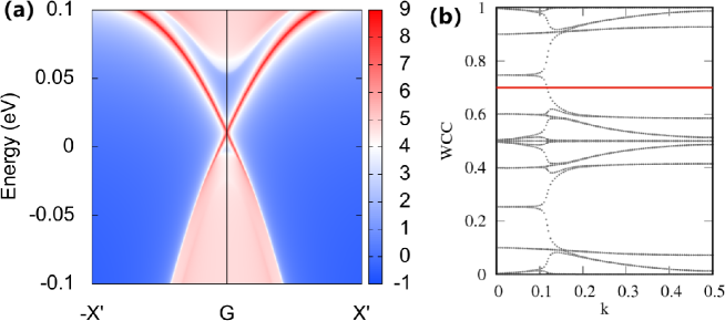
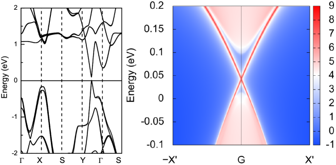
The energy band structures of VCClBr by using GGA and GGA+SOC are plotted in Figure 3. In the absence of SOC, the VCClBr is a direct gap semiconductor with the gap of 57 meV, and the valence band maximum (VBM) and conduction band minimum (CBM) locate at the one point along -Y path. It clearly seen that the very strong anisotropy is observed for energy band structures along -X and -Y paths. When including SOC, the VCClBr is still a direct gap semiconductor, and the gap is improved to 76 meV. The previous calculated results show that is a QSHIw-1 . The Janus monolayer as a derivative of centrosymmetric QSHI is a normal insulator, which can be reverted by straingsd4 . However, Janus monolayer still maintains nontrivial topological properties from QSHI (X=Sb and Bi) with inversion symmetrygsd5 . To confirm the topological properties of VCClBr, the topological invariant is calculated. For a material with inversion symmetry, topological invariant can be attained from the product of parities of all occupied states at four time-reversal-invariant-momentum points in the 2D BZ. However, VCClBr is non-centrosymmetrical, and the can be verified by the calculation of Wannier charge center (WCC). If equals 1/0, a material is a topologically nontrivial/trivial state. As plotted in Figure 4, an arbitrary reference line crosses the evolution lines of WCC an odd number of times, giving rise to =1, which indicates that VCClBr is a QSHI. Furthermore, a QSHI should exhibit non-trivial topological edge states. We further calculate one-dimensional edge states on (100) edge, which are plotted in Figure 4. It is clearly seen that topological helical edge states with the appearance of the Dirac cone connect the conduction and valence bands. The HSE06 is also employed to check the reliability of nontrivial topological properties of VCClBr. Within HSE06+SOC, the energy band structure and one-dimensional edge states are plotted in Figure 5. Calculated results show that the gap of VCClBr is improved to 87 meV from 76 meV with GGA+SOC, and the nontrivial topological properties are still kept with topological helical edge states.
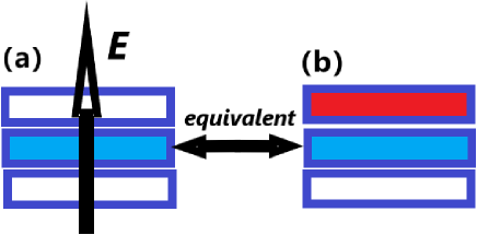
The is a Dirac semimetal without considering SOC, and no opened gap is observedw-1 . Compared to , VCClBr lacks horizontal mirror symmetry, possessing a built-in electric field, which induces the opened gap. To confirm this, we apply an external electric field () perpendicular to the , which should induce a gap. Since the electric field is a vector (not a pseudovector), the horizontal mirror symmetry will be broken by electric field. This is different from the magnetization as a pseudovector, which preserves the horizontal mirror symmetry. Thus, applying an external electric field can be used to simulate Janus structure (see Figure 6) in a sense.
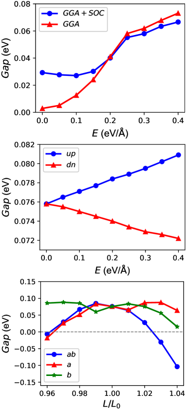
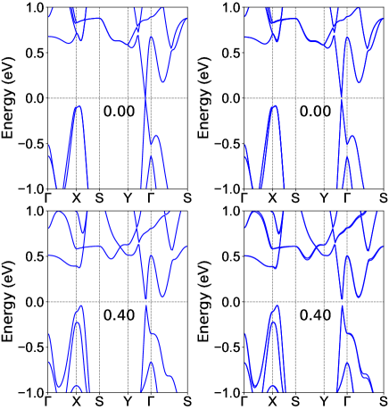
For monolayer, the evolution of band gap as a function of applied electric field is provided in Figure 7 by using GGA and GGA+SOC, and the representative energy bands under 0.00 eV/ and 0.04 eV/ electric field are plotted in Figure 8. In the absence of SOC, the band gap increases monotonously from 0 meV with increasing electric field for . This implies that applied electric field can induce the gap for , which is equivalent to a built-in electric field by constructing Janus structure, like VCClBr. For example 0.04 eV/ electric field, the gap of is 73 meV without considering SOC, and the GGA+SOC gap is reduced to 67 meV. It is noted that the gap with GGA+SOC is larger than one with GGA under small electric field, and then the opposite situation is observed with sequentially increasing electric field. Finally, the edge states are calculated within considered range. It is found that the nontrivial topological properties of are robust against applied electric field, and the representative topological helical edge states under 0.40 eV/ electric field are plotted in FIG.1 of electronic supplementary information (ESI).
The electric field effects on electronic and topological properties of VCClBr are also investigated. Janus VCClBr has different atomic species on its upper and lower facets (see Figure 6), which means that applying and directional electric field are not equivalent. This is different from , which has the same atomic species on its upper and lower facets (see Figure 6), giving rise to equivalent effects caused by applying both and directional electric field. The energy band gaps of VCClBr monolayer as a function of applied electric field along + and - directions by using GGA+SOC are plotted in Figure 7. The gap increases with increasing directional , while increasing directional reduces the gap. However, the gap change is very small with from 0.00 eV/ to 0.40 eV/, and only 5.1/-3.6 meV for and directional , which is very smaller than one (37.3 meV) of . It is also proved that the nontrivial topological properties of VCClBr are robust against applied electric field.
Strain is an effective method to tune electronic properties of 2D systems, and further affects their topological propertiesh1 ; h2 ; h3 . Here, both biaxial and uniaxial strains are considered to investigate the robustness of nontrivial topological properties of VCClBr. The is used to simulate compressive/tensile strain, where and are the strained and unstrained lattice constants, respectively. The 1 (1) means compressive (tensile) strain. For biaxial strain, the and lattice parameters simultaneously change, and atomic positions are allowed to relax. For uniaxial strain, the / lattice parameter changes, and the / lattice parameter and atomic positions are allowed to relax in response to an applied in-plane uniaxial strain.
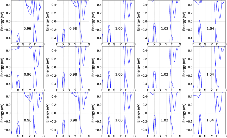
The electronic structures versus / are calculated by using GGA+SOC. The variation of band gaps with biaxial, uniaxial- and uniaxial- cases are plotted in Figure 7, and the energy band structures at representative applied strain are shown in Figure 9. For biaxial strain, with increasing strain, the gap firstly increases, and then decreases, which is due to the transition of CBM from one point along -S to one point along -Y. It is found that both compressive and tensile strains can induce semiconductor-metal transitions, which are due to the variation of CBM and VBM. Our calculated results show that the nontrivial topological properties are robust within considered strain range. For 0.96 or 1.04 strain, VCClBr is a metal, but the gap along -Y path is still maintained, and topological helical edge states still exist (see FIG.2 of ESI). Partly, the uniaxial- compressive/tensile strain is equivalent to uniaxial- tensile/compressive one, which can be confirmed by their gaps versus . It is found that uniaxial strain can also induce the change of CBM or VBM, giving rise to nonmonotonic dependence of gap on . Semiconductor-metal transitions can also be observed at uniaxial- 0.96 strain. However, the gap along -Y path always exists. The topological helical edge states can always be observed with considered uniaxial strain range, which are plotted in FIG.3 and FIG.4 of ESI at 0.96 and 1.04 strains.
| Name | ||||||||||||
|---|---|---|---|---|---|---|---|---|---|---|---|---|
| VCClBr | 130.67 | 17.08 | 215.81 | 53.45 | -0.612 | 0.019 | -0.593 | -0.513 | -0.032 | -0.545 | -0.425 | -0.219 |
| VCFBr | 151.06 | 21.42 | 229.97 | 54.47 | -1.957 | 0.115 | -1.842 | -1.669 | -0.243 | -1.912 | -1.116 | -0.727 |
| VCFCl | 161.47 | 23.10 | 229.17 | 55.06 | -1.359 | 0.165 | -1.194 | -1.135 | -0.176 | -1.311 | -0.667 | -0.505 |
V Piezoelectric properties
For noncentrosymmetric material, an applied strain or stress can induce electric dipole moments and produce electricity, called piezoelectric effect. The pristine is non-piezoelectric, while VCClBr with particular Janus structure possessess piezoelectric effect. The third-rank piezoelectric stress tensor and strain tensor can be used to describe piezoelectric response of a material. The relaxed piezoelectric tensors ( and ) are obtained as the sum of ionic and electronic contributions:
| (5) |
and
| (6) |
Where , and are polarization vector, strain and stress, respectively, and the superscripts and mean electronic and ionic contributions. The and ( and ) are also called clamped-ion (relax-ion) piezoelectric coefficients. The and can be connected by elastic tensor :
| (7) |
For 2D materials, these conditions ( ==0 for i=3 or j=3) are assumed, which implies that only the in-plane strain and stress are taken into account. However, the polarization can be allowed to remain out-of-plane. We define the in-plane directions and as the short edge and long edge direction of primitive cell, and as perpendicular to the 2D layer. Employing Voigt notation, the piezoelectric stress and strain tensors due to point group symmetry can be reduced into :
| (8) |
| (9) |
When a uniaxial in-plane strain is applied, only a vertical piezoelectric polarization exists (0 or 0). Moreover, with applied biaxial in-plane strain, the superposed out-of-plane polarization will arise (0 and 0). The and can be directly calculated by DFPT, and the and can be derived by Equation 1, Equation 7, Equation 8 and Equation 9:
| (10) |
| (11) |
The calculated () is -0.593 C/m (-0.545 C/m) with ionic part 0.019 C/m (-0.032 C/m) and electronic part -0.612 C/m (-0.513 C/m). The electronic and ionic polarizations of have opposite signs, while they have the same signs for . However, the electronic contribution dominates the piezoelectricity of both and . Based on Equation 10 and Equation 11, the and can be attained from previous calculated and . The calculated () is -0.425 pm/V (-0.219 pm/V), which are higher than or compared with ones of other 2D materialsq7 ; q9 . The is almost twice as large as , which is mainly due to very different and . Thus, VCClBr is a potential PQSHI.
VI Discussions and Conclusion
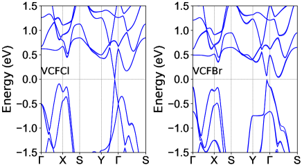
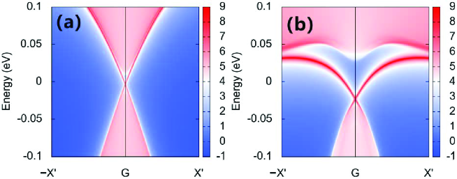
The (Y=F, Cl, Br and I) monolayers have been predicted to be topological Dirac semimetals without SOCw-1 . However, for , the Fermi level deviates from Dirac point. Thus, based on (Y=F, Cl and Br) monolayers, we construct another two Janus monolayer VCFBr and VCFCl of VCXY (XY=F, Cl and Br). The optimized lattice constants and are listed in Table 1. It is found that increases with the size of X and Y anions (from VCFCl to VCFBr to VCClBr), while is less affected, which is because the X and Y anions are directly bonded to V atoms along direction. The energy band structures of VCFBr and VCFCl within SOC are plotted in Figure 10. Calculated results show that VCFCl and VCClBr are direct gap semiconductors, while VCFBr is an indirect gap semiconductor. The CBM of VCFBr is at one point along -S path, while the VBM locates at one point along -Y path. For VCFCl and VCClBr, both CBM and VBM locate at one point along -Y path. As summarized in Table 1, the gap increases with the size of X and Y anions (from VCFCl to VCFBr to VCClBr). It is clearly seen that topological helical edge states connect the valence and conduction bands of VCFBr and VCFCl (see Figure 11), confirming their nontrivial topological properties.
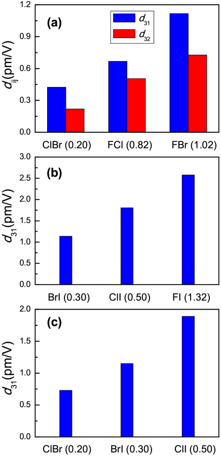
For monolayer VCClBr, VCFBr and VCFCl, the calculated elastic constants , piezoelectric stress coefficient along with electronic and ionic parts, and piezoelectric strain coefficient are listed in Table 2. For these monolayers, calculated elastic constants satisfy mechanical stability criteria, confirming their mechanical stabilities. For all these monolayers, the electronic and ionic contributions of have opposite signs, while they have the same signs for , and the electronic part dominates and . For three monolayers, the is larger than . The and of VCFBr are the largest among these monolayers, which may be due to very different electronegativities of F and Br atoms compared with F and Cl or Cl and Br atoms. The and (absolute value) of VCXY (XY=F, Cl and Br) along with the electronegativity difference of X and Y atoms are plotted in Figure 12. Similar phenomenon can be found in monolayer (X=F, Cl and Br; Y=I) and NiXY (XY=Cl, Br and I)w-2 ; w-3 , and their along with the electronegativity difference of X and Y atoms are also plotted in Figure 12. It is clearly seen that the large electronegativity difference of X and Y atoms is related with large out-of-plane piezoelectric response. It is noted that the of VCFBr is larger than 1.0 pm/V, which is rare for out-of-plane piezoelectric response of 2D systems. Finally, the phonon dispersions of VCFBr and VCFCl are calculated, which are plotted in FIG.5 of ESI. Unfortunately, the two monolayers are dynamically unstable due to existing imaginary frequencies. However, these comparisons provide some thoughts and scientific basis for searching large out-of-plane piezoelectric response in Janus 2D materials.
In summary, we have demonstrated coexistence of piezoelectricity and robust nontrivial band topology in Janus VCClBr monolayer with dynamical, mechanical and thermal stabilities based on the reliable DFT calculations. The nontrivial band topology in Janus VCClBr monolayer is confirmed by topological helical edge states, which is robust against strain and external electric field. Only out-of-plane piezoelectric response exists due to broken horizontal mirror symmetry. The predicted out-of-plane and are higher than or comparable with ones of many 2D known materials, which is highly desirable for ultrathin piezoelectric devices. It is found that the elastic, electronic and piezoelectric properties of VCClBr monolayer show very strong anisotropy due to the Cl and Br anions directly bonded to V atoms along the direction. Our predicted VCClBr provides a possible platform to future development of multifunctional piezoelectronics, and these findings open new idea to realize PQSHI with large out-of-plane piezoelectric response.
Acknowledgements.
This work is supported by Natural Science Basis Research Plan in Shaanxi Province of China (2021JM-456). We are grateful to the Advanced Analysis and Computation Center of China University of Mining and Technology (CUMT) for the award of CPU hours and WIEN2k/VASP software to accomplish this work.References
- (1) W. Wu and Z. L. Wang, Nat. Rev. Mater. 1, 16031 (2016).
- (2) C. F. Wang, H. J. Li, M. G. Li et al., Adv. Funct. Mater. 315, 2009457 (2021).
- (3) W. Wu, L. Wang, Y. Li, F. Zhang, L. Lin, S. Niu, D. Chenet, X. Zhang, Y. Hao, T. F. Heinz, J. Hone and Z. L. Wang, Nature 514, 470 (2014).
- (4) K. N. Duerloo, M. T. Ong and E. J. Reed, J. Phys. Chem. Lett. 3, 2871 (2012).
- (5) L. Dong, J. Lou and V. B. Shenoy, ACS Nano, 11, 8242 (2017).
- (6) R. X. Fei, We. B. Li, J. Li and L. Yang, Appl. Phys. Lett. 107, 173104 (2015).
- (7) M. N. Blonsky, H. L. Zhuang, A. K. Singh and R. G. Hennig, ACS Nano, 9, 9885 (2015).
- (8) S. D. Guo, Y. T. Zhu, W. Q. Mu and W. C. Ren, EPL 132, 57002 (2020).
- (9) Y. Guo, S. Zhou, Y. Z. Bai, and J. J. Zhao, Appl. Phys. Lett. 110, 163102 (2017).
- (10) W. B. Li and J. Li, Nano Res. 8, 3796 (2015).
- (11) C. L. Kane and E. J. Mele, Phys. Rev. Lett. 95, 226801 (2005).
- (12) M. Konig, S. Wiedmann, C. Brune et al., Science 318, 766 (2007).
- (13) I. Knez, R. R. Du and G. Sullivan, Phys. Rev. Lett. 107, 136603 (2011).
- (14) C. C. Liu, W. Feng, Y. Yao, Phys. Rev. Lett. 107, 076802 (2011).
- (15) S. Murakami, Phys. Rev. Lett. 97, 236805 (2006).
- (16) S. Zhou, C. C. Liu, J. J. Zhao and Y. G. Yao, npj Quant. Mater. 3, 16 (2018).
- (17) Y. Xu, B. Yan, H. J. Zhang et al., Phys. Rev. Lett. 111, 136804 (2013).
- (18) H. M. Weng, X. Dai and Z. Fang, Phys. Rev. X 4, 011002 (2014).
- (19) J. J. Zhou, W. X. Feng, C. C. Liu, S. Guan and Y. G. Yao, Nano Lett. 14, 4767 (2014).
- (20) S. D. Guo, W. Q. Mu, X. B. Xiao and B. G. Liu, Nanoscale 13, 12956 (2021).
- (21) S. D. Guo, W. Q. Mu, M. Y. Yin, Y. C. Li and W. C. Ren, J. Phys. D: Appl. Phys. 54, 505006 (2021).
- (22) S. D. Guo, Y. T. Zhu, W. Q. Mu and X. Q. Chen, J. Mater. Chem. C 9, 7465 (2021).
- (23) A.-Y. Lu, H. Zhu, J. Xiao, C.-P. Chuu, Y. Han, M.-H. Chiu, C.-C. Cheng, C.-W. Yang, K.-H. Wei, Y. Yang, Y. Wang, D. Sokaras, D. Nordlund, P. Yang, D. A. Muller, M.-Y. Chou, X. Zhang and L.-J. Li, Nat. Nanotechnol. 12, 744 (2017).
- (24) J. Zhang, S. Jia, I. Kholmanov, L. Dong, D. Er, W. Chen, H. Guo, Z. Jin, V. B. Shenoy, L. Shi and J. Lou, ACS Nano 11, 8192 (2017).
- (25) H. W. Xu, H. Wang, J. Zhou, Y. F. Guo, J. Kong and J. Li, npj Computational Materials 7, 31 (2021).
- (26) Y. H. Li, Y. F. Zhang, J. Deng, W. H. Dong, J. T. Sun, J. B. Pan and S. X. Du, J. Phys. Chem. Lett. 13, 3594 (2022).
- (27) S. D. Guo, X. S. Guo, X. X. Cai, W. Q. Mu and W. C. Ren, J. Appl. Phys. 129, 214301 (2021).
- (28) S. D. Guo, Y. T. Zhu, K. Qin and Y. S. Ang, Appl. Phys. Lett. in press (2022).
- (29) P. Hohenberg and W. Kohn, Phys. Rev. 136, B864 (1964); W. Kohn and L. J. Sham, Phys. Rev. 140, A1133 (1965).
- (30) G. Kresse, J. Non-Cryst. Solids 193, 222 (1995).
- (31) G. Kresse and J. Furthmller, Comput. Mater. Sci. 6, 15 (1996).
- (32) G. Kresse and D. Joubert, Phys. Rev. B 59, 1758 (1999).
- (33) J. P. Perdew, K. Burke and M. Ernzerhof, Phys. Rev. Lett. 77, 3865 (1996).
- (34) J. Heyd, G. E. Scuseria and M. Ernzerhof, J. Chem. Phys. 124, 219906 (2006)
- (35) A. Togo, F. Oba, and I. Tanaka, Phys. Rev. B 78, 134106 (2008).
- (36) X. Wu, D. Vanderbilt and D. R. Hamann, Phys. Rev. B 72, 035105 (2005).
- (37) Q. Wu, S. Zhang, H. F. Song, M. Troyer and A. A. Soluyanov, Comput. Phys. Commun. 224, 405 (2018).
- (38) A. A. Mostofia, J. R. Yatesb, G. Pizzif, Y.-S. Lee, I. Souzad, D. Vanderbilte and N. Marzarif, Comput. Phys. Commun. 185, 2309 (2014).
- (39) E. Cadelano and L. Colombo, Phys. Rev. B 85, 245434 (2012).
- (40) E. Cadelano, P. L. Palla, S. Giordano, and L. Colombo, Phys. Rev. B 82, 235414 (2010).
- (41) S. D. Guo and Y. T. Zhu, J. Phys.: Condens. Matter 34, 235501 (2022).
- (42) H. Huan, Y. Xue, B. Zhao, G. Y. Gao, H. R. Bao and Z. Q. Yang, Phys. Rev. B 104, 165427 (2021).
- (43) X. Zhou, R. Zhang, Z. Zhang, W. Feng, Y. Mokrousov and Y. Yao, npj Comput. Mater. 7, 160 (2021).
- (44) S. D. Guo, W. Q. Mu and B. G. Liu, 2D Mater. 9, 035011 (2022).