Transport spectroscopy of ultraclean tunable band gaps in bilayer graphene
Abstract
The importance of controlling both the charge carrier density and the band gap of a semiconductor cannot be overstated, as it opens the doors to a wide range of applications, including, e.g., highly-tunable transistors, photodetectors, and lasers. Bernal-stacked bilayer graphene is a unique van-der-Waals material that allows tuning the band gap by an out-of-plane electric field. Although the first evidence of the tunable gap was already found ten years ago, it took until recent to fabricate sufficiently clean heterostructures where the electrically induced gap could be used to fully suppress transport or confine charge carriers. Here, we present a detailed study of the tunable band gap in gated bilayer graphene characterized by temperature-activated transport and finite-bias spectroscopy measurements. The latter method allows comparing different gate materials and device technologies, which directly affects the disorder potential in bilayer graphene. We show that graphite-gated bilayer graphene exhibits extremely low disorder and as good as no subgap states resulting in ultraclean tunable band gaps up to 120 meV. The size of the band gaps are in good agreement with theory and allow complete current suppression making a wide range of semiconductor applications possible.
pacs:
Valid PACS appear hereI Introduction
Bernal stacked bilayer graphene (BLG) is a unique material: intrinsically it is a 2D semi-metal, but it can be turned into a 2D semiconductor by applying an external out-of-plane electric field McCann2006Mar ; Min2007 ; McCann_2013 , with an electronic band gap that is directly related to the strength of the displacement field. The underlying mechanism of the band gap opening is a textbook example of how the breaking of inversion symmetry results in a gap in the electronic band structure. The first experimental evidence of the tunable band gap in BLG was obtained by angle-resolved photoemission spectroscopy Ohta2006 ; Zhou2007Oct and infrared spectroscopy experiments Mak2009 ; Kuzmenko2009Mar ; Zhang2009Jun , where band gaps up to 250 meV have been reported. Signatures of the tunable band gap have also been observed by scanning tunneling spectroscopy Yankowitz2014Sep ; Holdman2019Oct and in early transport measurements Oos2007Dec ; Szafranek2010Mar ; Xia2010Feb ; Szafranek2011Jul ; Lee2012Dec ; Miyazaki2010 ; Yan2010Nov ; Zou2010Aug ; Taychatanapat_PhysRevLett2010 ; Jing2010Oct ; Kanayama2015 . However, in the latter experiments, subgap states caused by disorder made it impossible to completely suppress the electron conduction Connolly2012Nov , making such BLG devices not suitable for semiconductor applications.
This shortcoming was solved neither by fabricating double-gated structures based on suspended BLG Weitz2010 ; Allen2012Jul ; Velasco2014 ; Ki2014 nor by encapsulating BLG into hexagonal boron nitride (hBN) Zhu2017Feb ; Goossens2012Aug ; Shimazaki2015 ; Sui_nature2015 . Only recently, with the use of graphite gates, the fabrication technology has advanced to the level where it is possible to open a gate-controlled band gap that results in a true band insulating state in BLG Li2016 ; Overweg2018Jan .
Here, we exploit this fabrication technology and show that the tunable band gap of BLG can finally also be directly observed in finite bias transport spectroscopy measurements. The obtained band gaps are in good agreement with theory as well as with the values extracted from thermally activated transport Shimazaki2015 ; Sui_nature2015 ; Taychatanapat_PhysRevLett2010 ; Zou2010Aug ; Yan2010Nov ; Jing2010Oct ; Miyazaki2010 ; Kanayama2015 . Most interestingly, we use finite bias spectroscopy, to systematically compare different double-gated BLG/hBN device technologies, as this method allows to sensitively probe hopping-transport due to potential disorder or impurity states, which both can result in effective subgap and tail states. The investigated devices differ mainly in the bottom gate material (graphite, gold, or highly doped silicon) and in the corresponding fabrication process. We show that the fabrication technology sensitively impacts the maximum device resistance and the presence and outline of diamonds of strongly suppressed conductance for finite bias voltage when measuring transport through electrostatically gapped BLG, as well as the tunability of the band gap with the electric displacement field.
We find that BLG devices with a graphite gate behave very closely to what theory predicts for ideal BLG, showing a truly semiconducting behavior in the presence of an applied displacement field. In the gapped regime, we measure maximum resistance values on the order of 100 G (limited only by the measurement setup), and we observe no appreciable signature of trap or impurity states with subgap energy. In contrast, both silicon and gold-gated devices appear to be affected by subgap states and disorder, but to different degrees. While very high gap-induced resistances are still observed in gold-gated devices, where the band gap just appears to be reduced in finite bias measurements, no gap can be directly observed in silicon-gated devices. All this confirms that the intrinsic properties of BLG become exploitable in graphite-gated BLG/hBN heterostructures, which therefore represents the most promising platform to unleash the potential of this unique tunable 2D semiconductor with interesting applications for THz electronics, quantum technologies, and mesoscopic physics.
II An electrostatically tunable band gap
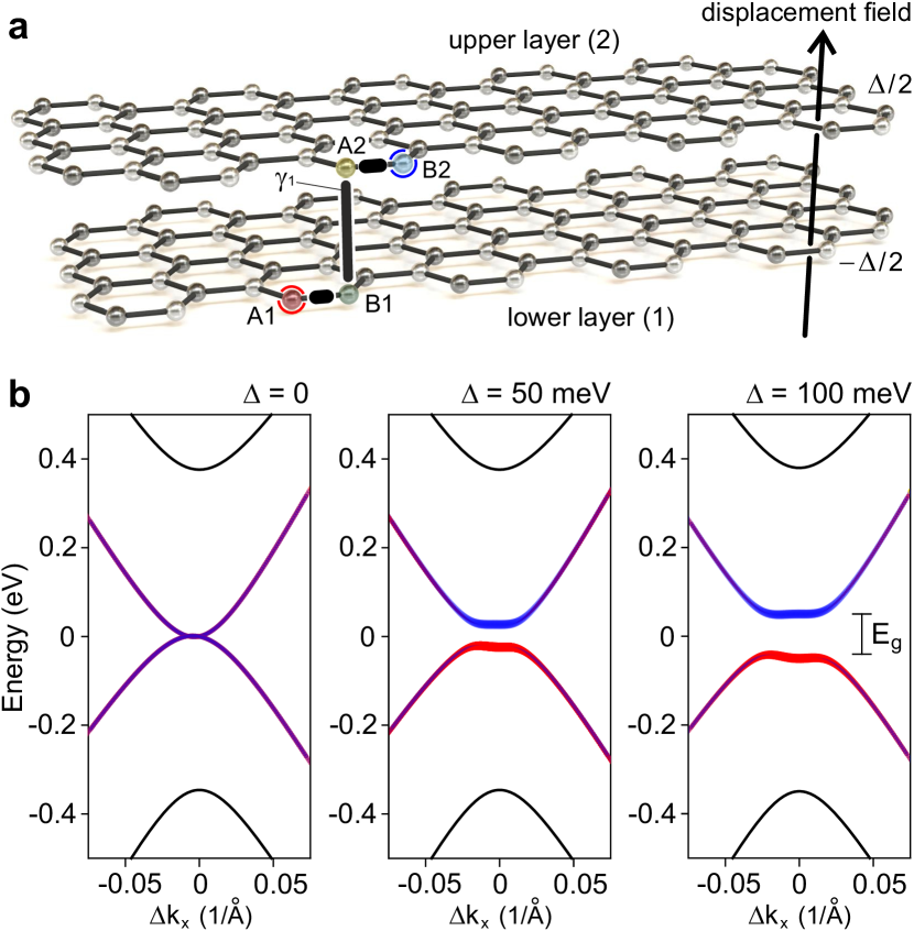
The inversion symmetry and its controlled breaking play an important role in determining the properties of intrinsic and gapped BLG. In the intrinsic form, the orbitals of the carbon atoms A1 and B2, which are responsible for the low energy spectra of BLG, are inversion-symmetric, and BLG is a semi-metal (see Figures 1a,b) Min2007 ; McCann_2013 . The symmetry is broken in the presence of an external out-of-plane displacement field, which induces an onsite potential difference between the upper and lower graphene layer. This potential difference leads in turn to the appearance of a band gap between the conductance and the valence band McCann2006Mar ; Min2007 ; McCann_2013 , as illustrated in Figure 1b. The size of the band gap, , depends on the onsite potential difference as McCann_2013 ; Min2007 :
| (1) |
where eV is the interlayer coupling strength Kuzmenko2009Nov ; Joucken2020 ; Jung2014Jan ; McCann_206 . The dependence between and the external electric displacement field is however non-trivial, as depends also on the screening of the charge carriers on the layers of BLG, which is influenced in turn by the onsite potential difference , thus requiring a self-consistent analysis McCann_2013 ; Slizovskiy2021 .
Different models have been used to calculate the dependence of the interlayer asymmetry on the applied out-of-plane displacement field , either using a simple plate-capacitor model with Hartree screening McCann2006Mar ; McCann_2013 or, more recently, by additionally taking into account the layer-dependent out-of-plane polarization of the carbon orbitals Slizovskiy2021 . In both cases can be expressed as
| (2) |
where nm is the interlayer spacing of BLG, is the (magnitude of the) elementary charge, and are effective dielectric constants. In the model of Ref. McCann2006Mar ; McCann_2013 , , where is the effective dielectric constant of BLG Kumar2016 ; Jung2017 ; Island2019 . In contrast, in Ref. Slizovskiy2021 is the effective out-of-plane dielectric susceptibility of graphene and . Finally, is the difference between the charge carrier density in the upper and lower layer, whose detailed expression also depends on the considered model (see Supplementary Material). Below we will make use of both models when comparing theory with experiment.
II.1 Double-gated BLG devices
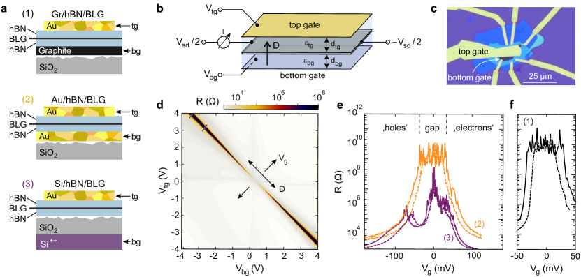
Experimentally, the way to apply an out-of-plane electric field to BLG and to control independently its chemical potential is to embed it into a plate capacitor, i.e., to have a bottom and a top gate (see Figures 2a,b). In this work, we compare devices fabricated with three different technologies. All devices are based on BLG encapsulated into hexagonal boron nitride and have a metallic top gate (tg), but differ in the bottom gate (bg), as illustrated in Figure 2a. Specifically, we consider devices with a graphite bottom gate (referred to as “Gr/hBN/BLG” or class 1 devices), devices with a gold (Au) bottom gate (referred to as “Au/hBN/BLG” or class 2 devices), and devices that use the heavily doped silicon substrate as bottom gate (referred to as “Si/hBN/BLG” or class 3 devices). An optical image of a final device with an Au bottom gate based on a stack-flipping process is shown in Figure 2c. It is worth noting here that although the Au gate/stack-flipping process results in less disorder than directly placing an hBN/BLG/hBN stack on a (rough) Au bottom gate, the Au top gate (used in all devices) has overall less detrimental effect on device quality, which is due to the fact that the BLG heterostructure no longer needs to be moved afterwards. Details on the device fabrication are given in the Supplementary Material.
In the investigated devices, the top gate is narrower than the bottom gate, and the BLG regions doped exclusively by the bottom gate act as leads. In the double-gated region, the voltages and applied to the top and to the bottom gate induce a displacement field through the BLG:
| (3) |
where are the offset of the charge neutrality point (CNP) from , and and are the lever-arms determined by the capacitive coupling of the top and bottom gate, respectively (, are the dielectric constants and , the thicknesses of the dielectric layers; see Figure 2b). The effect of the voltages and on the chemical potential in the double-gated region is understood at best in terms of the effective gate voltage
| (4) |
where is the ratio of the two lever-arms. This effective gate voltage is defined such that is directly linked to the electro-chemical potential via , as long as is within the band gap. Also allows to change the total charge carrier density outside the band gap by , if both layers are on the same potential (for more details see Supplementary Material). For all devices, we extract the values of and from resistance-map measurements, and the value of either or from quantum Hall measurements Zhao2010 ; SonntagMay2018 ; Schmitz2020 (see Supplementary Material).
II.2 Resistance maps and maximal resistance
As a first step to characterize the double-gated BLG devices, we record resistance maps like the one of Figure 2d, by applying a small source-drain bias and by measuring the current as a function of and (see schematic in Figure 2b). The resistance maps exhibit two distinct features: (I) A diagonal line of elevated resistance , which marks the shifting of the charge neutrality point of the BLG in the double-gated region as a function of and . This line represents the axis (i.e., ). The slope of this line is directly given by the ratio of the lever arms . For example, for the measurement shown in Figure 2d, it is , indicating a very symmetric capacitive coupling of the top and bottom gate. (II) Along this diagonal line the maximum resistance strongly increases while increasing the magnitude of the displacement field, which is a hallmark of the opening of the band gap induced by the displacement field.
While these qualitative features are common to the resistance maps performed on devices of all three different classes (for a comparison of carrier mobilities see Supplementary Material), the differences between the three technologies become apparent when comparing line traces of the resistance measured as a function of at fixed -fields, see Figures 2e,f. In all cases, we observe an abrupt decrease of the largest resistance around . But, while devices with a graphite and gold bottom gate show well-defined plateaus of high resistance (see Figure 2f and orange traces in Figure 2e), the resistance of the device with a silicon bottom gate is significantly lower and varies by more than three orders of magnitude within the gate voltage range where the band gap is expected (purple traces in Figure 2e). These strong variations and the reduced maximum-resistance can be explained in terms of hopping transport through subgap states caused by the disorder due to charged impurities in the SiO2, at the SiO2/hBN interfaces, or at the unscreened BLG edges Oos2007Dec ; Miyazaki2010 ; Zou2010Aug ; Yan2010Nov ; Taychatanapat_PhysRevLett2010 ; Kanayama2015 ; Zhu2017Feb which create spatial electrostatic variations along the transport channel and are the main origin of the observed disorder potentials (see also discussion in Sec. IV). Vice versa, the high-resistance plateaus observed in devices with graphite or a gold bottom gate suggest that the chemical potential is tuned through a clean band gap, with few or no subgap states. For both types of devices, the width of the high-resistance plateau – i.e., the size of the band gap – increases as expected with increasing displacement field (see dashed and solid resistance traces in Figure 2e,f). However, devices with a graphite bottom gate exhibit a much sharper onset of the plateau and slightly higher values of resistance than those with a gold bottom gate, indicating that graphite gates are more effective than metallic ones at suppressing residual charge transport through the band gap and particularly near the band edges. This difference can be attributed to the disorder, i.e. spatial electrostatic variations along the BLG transport channel, caused (I) by the fabrication process of the Au-gated devices, which is more prone to interface contamination, or (II) ultimately by grain boundaries in the gold itself Osvald1992 .
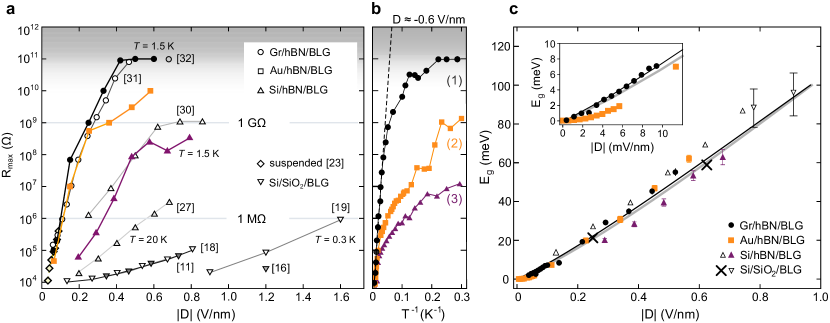
The different performance of the three technologies becomes even more apparent by plotting the maximum resistance as a function of the displacement field , see Figure 3a (for more details on why is a good quantity, see Supplementary Material). In this plot, we report both data from three devices measured in our lab (colored data points), as well as data taken from literature (open data points). This overview plot shows that the maximum resistance attainable for a given value of strongly depends on the fabrication technology used for the double-gated BLG devices. Devices, where BLG is directly placed on SiO2, require high displacement fields V/nm to reach moderate values of 1 M. Encapsulating BLG between hBN layers already helps reducing the disorder potential and allows achieving maximum resistances in the range of 100 M 1 G at -fields of around V/nm (and a temperature of K). The observed saturation of for higher -fields can be explained by disorder-induced hopping transport at subgap energies and along the edges of the BLG Oos2007Dec ; Miyazaki2010 ; Zou2010Aug ; Yan2010Nov ; Taychatanapat_PhysRevLett2010 ; Kanayama2015 ; Zhu2017Feb . The use of a metallic gate allows to reach values of as high as 10 G at moderate values of , but it is only the use of a graphite gate that allows to open a real clean band gap and to completely suppress the current at reasonably low -fields, reaching G – which represents also the maximum value of resistance measurable in our experimental setup. The values of measured in our Gr/hBN/BLG device compare well with the data of Ref. Overweg2018Jan ; Li2016 and, at low -fields, also with the values measured in a double-gated suspended BLG device (see diamond symbols in Figure 3a, taken from Ref. Weitz2010 ).
II.3 Thermally activated transport
The maximum resistance is, of course, a function of temperature. For the three devices illustrated in Figure 2a, we study the maximum resistance as a function of temperature for a fixed value of the displacement field . To extract information on the underlying transport mechanisms, we plot logarithmically as a function of , as shown in Figure 3b.
At low temperatures, K ( K-1), only weakly depends on , as predicted by both variable range hopping (VRH) Yan2010Nov ; Jing2010Oct and a combination of nearest-neighbor hopping and VRH Sui_nature2015 ; Zou2010Aug . In this regime, the values of observed for the three gating technologies differ by several orders of magnitude. The low resistance values at low temperature of the Si/hBN/BLG sample are reminiscent of those observed in disordered semiconductors Shklovskii1984 , where transport via impurity bands and hopping transport dominates. This notion is also in agreement with earlier studies Miyazaki2010 ; Kanayama2015 and with compressibility measurements Henriksen2010Jul ; Young2012Jun , which have shown that there is a large density of (localized) states in gapped BLG when placed on SiO2, resulting in low values of .
At high temperatures K (T K-1), for all types of devices the dependence of on is well described by thermally activated transport Shimazaki2015 ; Sui_nature2015 ; Taychatanapat_PhysRevLett2010 ; Zou2010Aug ; Yan2010Nov ; Jing2010Oct ; Miyazaki2010 ; Kanayama2015 , i.e., , where is the band gap energy and the Boltzmann constant. By fitting a line to the resistance data in the Arrhenius plot (see, e.g., dashed line in Figure 3b) we can extract at a given value of for the different devices. Repeating this type of fitting for different values of , we obtain the plot shown in Figure 3c. It can be observed, that the values of determined in this way for the different devices agree rather well with each other, independently of the fabrication technology. This is the case because at high temperatures the impact of localized subgap states is eventually smeared out by thermal excitations.
Our data agree also well with the band gaps reported by earlier experiments (see opens symbols and crosses in Figure 3c) Zhang2009Jun ; Yan2010Nov ; Sui_nature2015 and with the values predicted by theory. Here, we consider both the self-consistent solution of the plate-capacitor model with Hartree screening proposed by McCann and Koshino McCann_2013 with (black line in Figure 3c), as well as the more recent model of Ref. Slizovskiy2021 , which takes into account the layer-dependent polarization of the orbitals (gray line). In this case, we used for the effective out-of-plane dielectric susceptibility of graphene, see Equation (2). For the device with graphite back gate, the extracted values of agree well with theory even at very low displacement fields (see inset in Figure 3c).
III Direct observation of the band gap
Measurements like those presented in Figures 3b and 3c allow to extract the size of the electrostatically induced band gap, , but not to observe it directly. To directly probe the band gap, we use finite-bias spectroscopy at low temperatures, i.e., we measure the differential conductance of our devices, , as a function of and of . This is a sensitive method to probe the characteristic energy scales of a system and the presence of localized states.
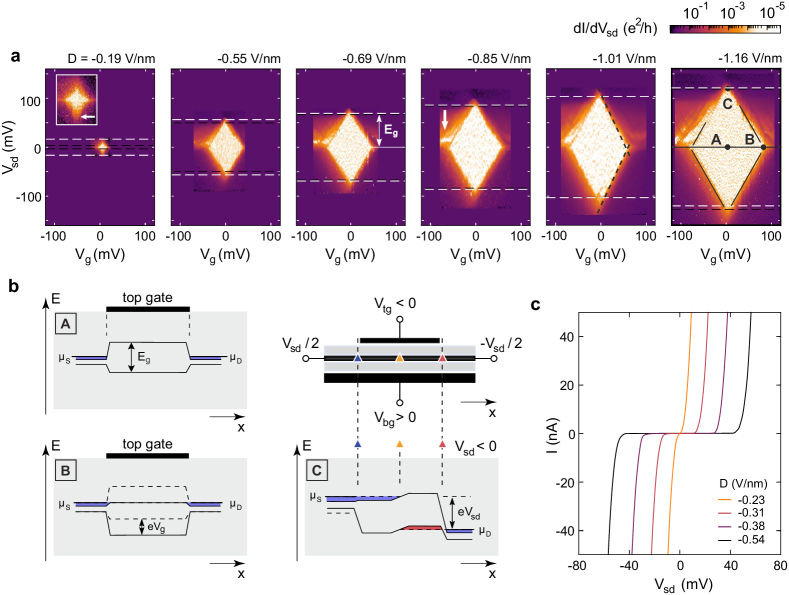
Figure 4a shows finite-bias spectroscopy measurements performed at mK in a device with a graphite gate, for different values of the displacement field . Diamond-shaped regions of strongly suppressed conductance can be observed around , where the size of the diamond scales with the applied -field. For large values of , the extent of the region of strongly suppressed conductance along the axis agrees very well with the size of the band gap predicted by theory, represented here by the horizontal white dashed lines.
The schematics of Figure 4b depict different characteristic regimes that correspond to the points marked with A, B, C in the rightmost panel of Figure 4a. Point A represents the condition of at the center of the diamond, where charge transport through the device is suppressed the most. Point B represents the onset of charge transport induced by tuning such that the conduction band in the double-gated area of the device is aligned with the conduction band of the leads. Point C represents the onset of conduction caused by a sufficiently large source-drain bias voltage applied symmetrically over the gated region (i.e.,
).
The source-drain voltage creates a p-n junction within the BLG, over which the complete drops as long as there is no current flowing (for more details see Supplementary Material). This results in the diode-like behavior of the bias-dependent current shown in Figure 4c, where the threshold voltage clearly depends on the -field and therefore on the size of the band gap.
Please note that the slight asymmetries in outside the diamonds with respect to V and (see e.g. white arrow in the 4th panel of Figure 4a) can be explained by the -field dependent layer polarization and a spatially varying disorder potential. For example, for negative displacement field the carriers near the valance band edge () are located in the upper BLG layer McCann_2013 ; Levitov2017 (see Fig. 1b), which is closer to the Au top gate. Thus, the asymmetry in indicates asymmetries in the residual disorder at the Au top and graphite bottom gate interface. The asymmetry in V indicates a spatial variation of disorder, as the location of the p-n junction underneath the top gate in this case depends on the polarity of V (for more details, see Supplementary Material).
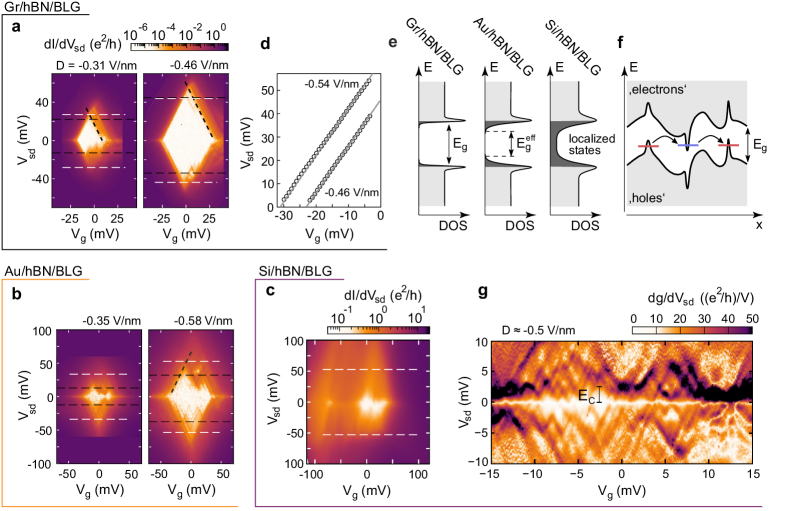
Figures 5a-c present the same type of bias-spectroscopy measurements performed at K on a second device with a graphite bottom gate (Figure 5a), as well as on a device with gold bottom gate (Figure 5b) and on one with silicon bottom gate (Figure 5c). Also at this higher temperature, the device with graphite bottom gate shows at large -fields a well-defined diamond-shaped region of strongly suppressed conductance around , whose span along the axis is in fairly good agreement with the size of the band gap predicted by theory (horizontal white dashed lines).
The slopes of the diamond outlines in the map is very close to 2 as highlighted by the dashed lines (see also the second rightmost panel in Figure 4a). In Figure 5d we show the extracted outline of the diamond (resistance threshold value of ) for two different displacement fields (see labels). In both cases, the slope agrees very well with a slope of 2 (see gray lines). This means that indeed tunes directly the chemical potential in the band gap region and no trap states need to be charged. The slope of 2 results from the fact that when starting in configuration A (see Figures 4a,b) we need either to lift the band gap (moving to point C) or (moving to point B) resulting in .
The fact that this can be observed, in turn, unambiguously indicates the absence of impurity bands, localized states or any other trap state that can potentially be charged in the device.
The device with a gold bottom gate presents also a region of strongly suppressed conductance for large -fields. However, this does not appear as a single, well-defined diamond, but as a series of overlapping diamonds with different sizes and positions (see right panel of Figure 5b). The device with silicon bottom gate shows overall much higher conductance, with no clear feature that can be related to the band gap energy (Figure 5c).
As already discussed in Section II, the different behavior of the three devices can be traced back to their different level of disorder. In the device with a silicon bottom gate, the unscreened potential of charges trapped in the SiO2 substrate or at the SiO2/hBN interfaces creates localized states with subgap energies Ando2006 ; Ishigami2007 ; Chen2008Mar ; Morozov2008 ; Zhang2009Aug ; Dean2010 , as sketched in Figures 5e,f. Signatures of hopping transport can indeed be found in the derivative of the differential conductance , see Figure 5g. Here, we observe diamond-like features associated to the charging of charge islands or of individual localized states, as characteristic for statistical Coulomb blockade Stampfer2009Feb ; Gallagher2010Mar . The extent of these diamond features in is related to the characteristic charging energy of a localized state, a charge puddle, or to the energy spacing between different states. Here, we find typical energies in the range of 2-3 meV. The observation of individual charging events indicates that the total number of localized states (or puddles) contributing to transport is rather limited. Nevertheless, these states provide a percolation channel through the gated BLG region and prevent a complete current suppression, in good agreement with earlier reports Zou2010Aug ; Taychatanapat_PhysRevLett2010 ; Kanayama2015 ; Sui_nature2015 .
The presence of a local bottom gate – either of gold or graphite – strongly screens the disorder potential caused by charged impurities and allows to open a real band gap in BLG by means of a displacement field. However, the band gap is ultraclean only in the case of devices with a graphite gate, while the device with a gold gate still presents signatures of transport through localized states with subgap energies. The presence of these localized states results in tail states in the density of states (DOS), which reduce or – in the case of silicon-gated devices – effectively suppress the band gap (see schematics in Figure 5e).
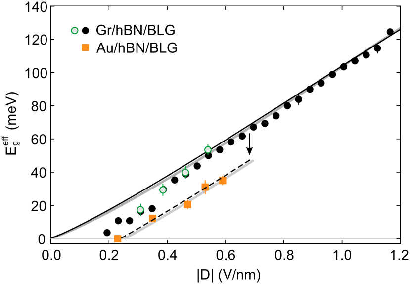
To quantitatively compare the band gaps observed by transport spectroscopy with theory, we define the effective band gap , where are the values of at which the differential conductance is equal to S at . These threshold voltages are indicated as dashed black lines in Figure 4a and Figures 5a,b. Note that the differential conductance of the Si/hBN/BLG device is always higher than S. Figure 6 shows the values of the effective gap as a function of the displacement field for two devices with a graphite bottom gate and for one with a gold bottom gate. For the devices with a graphite bottom gate, we observe an excellent agreement between the band gap measured by transport spectroscopy, , and the values predicted by theory for -fields larger than V/nm. The deviations at smaller values of indicate the presence of some residual disorder, whose influence is larger for small band gaps (see also inset of the leftmost panel in Figure 4a). Vice versa, for the device with a gold bottom gate the effective transport gap is around meV smaller compared to the expected values. This confirms the presence of extended tail states within the band gap, as sketched in Figure 5e. As for all devices the preparation of the BLG has been the same, rather than impurities or defects related to the BLG, these tail states are most likely induced by substrate roughness, or by contaminations at the interfaces due to the fabrication process of the gold-gated device Zibrov2017 ; Rhodes2019 ; Yankowitz2019 or by the disorder caused by grain boundaries in the gold Osvald1992 and are not caused by impurities or edge states in the BLG itself.
IV Summary and outlook
To conclude, we showed that finite-bias spectroscopy is a versatile method to characterize the band gap in BLG. Its high sensitivity allows comparing the influence of (electrostatic) disorder potentials for different gating-technologies. The measurements clearly indicate that devices with a graphite bottom gate fabricated as part of the van-der-Waals heterostructure outperform devices with gold and Si/SiO2 gates, and behave very closely to what theory predicts for ideal BLG. In graphite-gated devices, we achieve band gaps of about meV with resistances up to 100 G within the band gap (only limited by the setup). These results underline the importance of graphite as a bottom gate for BLG-based van-der-Waals heterostructures.
The high quality of Gr/hBN/BLG devices demonstrated in this work allows to readdress the broad field of possible applications offered by BLG, such as diodes Shioya2012Jan , phonon-lasers Kuzmenko2009Nov ; Tang2010Nov , hot-electron bolometers Yan2012Jul , field-effect transistors (FET) Cheli2009 ; Das2011Jan ; Sako2011Aug and tunnel FETs Alymov2016 . The latter two are especially interesting for terahertz (THz) detection, where graphene and BLG based devices have already shown promising results Dhillon2017 ; Bandurin2018 . The low disorder of Gr/hBN/BLG technology offers the possibility of significantly improving the device performance for this type of application, e.g., as recently demonstrated for tunnel FETs used for THz detection Gayduchenko2021 .
Other applications that can greatly profit from the excellent tunability of the band gap in Gr/hBN/BLG devices are those based on proximity-induced properties in BLG, such as superconductivity Kraft2018April ; Li2020May , exchange coupling Zollner2020Nov or strong spin-orbit coupling (SOC) Levitov2017 . For example, by placing a strong SOC material on top of BLG, only the band associated with the layer close to the SOC material will exhibit spin splitting, thanks to the layer dependence of the bands close to the K-point (see colors in Figure 1). This makes it possible to switch on and off the spin-orbit interaction by simply switching the sign of the -field Levitov2017 . Such an effect has been indeed recently demonstrated by taking advantage of the low disorder and the excellent control of the band gap with the applied -field in BLG devices with graphite gates Island2019 , which are therefore an interesting platform for spin-orbit valves and spin transistors Gmitra2017Oct .
Furthermore, Gr/hBN/BLG technology has allowed realizing sophisticated devices such as quantum point contacts Overweg2018Jan ; Kraft2018Dec ; Banszerus2020May ; Lee2020Mar , and quantum dots in BLG with single-electron control Eich2018Jul ; Banszerus2018Aug ; Banszerus2020Feb . This underlines the possibility of BLG as a potential host material for spin and valley qubits Wu2013 . Moreover, thanks to a long electron phase coherence length Engels2014Sep it promises to be an interesting platform for mesoscopic physics in low-dimensions.
In short, our study unambiguously shows that the Gr/hBN/BLG technology allows realizing van-der-Waals heterostructures that truly behave as semiconductors with an electrostatically tunable gap.
This opens up a wide field of possible applications, especially when considering that a required scalability can also be enabled by using high quality CVD BLG material Liu2012Sep ; Schmitz2017Jun ; Bisswanger2022Jun .
Acknowledgements The authors thank S. Trellenkamp, F. Lentz, and D. Neumaier for their support in device fabrication and F. Hassler, D. Kennes, A. Garcia-Ruiz and F. Haupt for discussions. This project has received funding from the European Union’s Horizon 2020 research and innovation program under grant agreement No. 881603 (Graphene Flagship) and from the European Research Council (ERC) under grant agreement No. 820254, the Deutsche Forschungsgemeinschaft (DFG, German Research Foundation) under Germany’s Excellence Strategy - Cluster of Excellence Matter and Light for Quantum Computing (ML4Q) EXC 2004/1 - 390534769, through DFG (BE 2441/9-1 and STA 1146/11-1), and by the Helmholtz Nano Facility Albrecht2017May . K.W. and T.T. acknowledge support from the Elemental Strategy Initiative conducted by the MEXT, Japan (Grant Number JPMXP0112101001) and JSPS KAKENHI (Grant Numbers 19H05790, 20H00354 and 21H05233).
Data availability The data supporting the findings are available in a Zenodo repository under accession code 10.5281/zenodo.6119509.
References
- (1) Edward McCann, Vladimir I. Fal’ko, Phys. Rev. Lett. 2006, 96, 086805.
- (2) Hongki Min, Bhagawan Sahu, Sanjay K. Banerjee, A. H. MacDonald, Phys. Rev. B 2007, 75, 155115.
- (3) E. McCann, M. Koshino, Rep. Prog. Phys. 2013, 76, 056503.
- (4) Taisuke Ohta, Aaron Bostwick, Thomas Seyller, Karsten Horn, Eli Rotenberg, Science 2006, 313, 951–954.
- (5) S. Y. Zhou, G.-H. Gweon, A. V. Fedorov, P. N. First, W. A. de Heer, D.-H. Lee, F. Guinea, A. H. Castro Neto, A. Lanzara, Nat. Mater. 2007, 6, 770–775.
- (6) Kin Fai Mak, Chun Hung Lui, Jie Shan, Tony F. Heinz, Phys. Rev. Lett. 2009, 102, 256405.
- (7) A. B. Kuzmenko, E. van Heumen, D. van der Marel, P. Lerch, P. Blake, K. S. Novoselov, A. K. Geim, Phys. Rev. B 2009, 79, 115441.
- (8) Yuanbo Zhang, Tsung-Ta Tang, Caglar Girit, Zhao Hao, Michael C. Martin, Alex Zettl, Michael F. Crommie, Y. Ron Shen, Feng Wang, Nature 2009, 459, 820–823.
- (9) Matthew Yankowitz, Joel I-Jan Wang, Suchun Li, A. Glen Birdwell, Yu-An Chen, Kenji Watanabe, Takashi Taniguchi, Su Ying Quek, Pablo Jarillo-Herrero, Brian J. LeRoy, APL Materials 2014, 2, 092503.
- (10) Gregory R. Holdman, Zachary J. Krebs, Wyatt A. Behn, Keenan J. Smith, K. Watanabe, T. Taniguchi, Victor W. Brar, Applied Physics Letters 2019, 115, 181601.
- (11) Jeroen B. Oostinga, Hubert B. Heersche, Xinglan Liu, Alberto F. Morpurgo, Lieven M. K. Vandersypen, Nat. Mater. 2008, 7, 151–157.
- (12) B. N. Szafranek, D. Schall, M. Otto, D. Neumaier, H. Kurz, Appl. Phys. Lett. 2010, 96, 112103.
- (13) Fengnian Xia, Damon B. Farmer, Yu-ming Lin, Phaedon Avouris, Nano Lett. 2010, 10, 715–718.
- (14) B. N. Szafranek, D. Schall, M. Otto, D. Neumaier, H. Kurz, Nano Lett. 2011, 11, 2640–2643.
- (15) Kayoung Lee, Babak Fallahazad, Hongki Min, Emanuel Tutuc, IEEE Trans. Electron Devices 2012, 60, 103–108.
- (16) Hisao Miyazaki, Kazuhito Tsukagoshi, Akinobu Kanda, Minoru Otani, Susumu Okada, Nano Lett. 2010, 10, 3888–3892.
- (17) Jun Yan, Michael S. Fuhrer, Nano Lett. 2010, 10, 4521–4525.
- (18) K. Zou, J. Zhu, Phys. Rev. B 2010, 82, 081407.
- (19) Thiti Taychatanapat, Pablo Jarillo-Herrero, Phys. Rev. Lett. 2010, 105, 166601.
- (20) Lei Jing, Velasco Jairo, Jr., Philip Kratz, Gang Liu, Wenzhong Bao, Marc Bockrath, Chun Ning Lau, Nano Lett. 2010, 10, 4000–4004.
- (21) K. Kanayama, K. Nagashio, Sci. Rep. 2015, 5, 1–9.
- (22) M. R. Connolly, R. K. Puddy, D. Logoteta, P. Marconcini, M. Roy, J. P. Griffiths, G. A. C. Jones, P. A. Maksym, M. Macucci, C. G. Smith, Nano Lett. 2012, 12, 5448–5454.
- (23) R. T. Weitz, M. T. Allen, B. E. Feldman, J. Martin, A. Yacoby, Science 2010, 330, 812–816.
- (24) M. T. Allen, J. Martin, A. Yacoby, Nat. Commun. 2012, 3, 934.
- (25) J. Velasco, Y. Lee, Z. Zhao, Lei Jing, P. Kratz, Marc Bockrath, C. N. Lau, Nano Lett. 2014, 14, 1324–1328.
- (26) D.-K. Ki, V. I. Fal’ko, D. A. Abanin, A. F. Morpurgo, Nano Lett. 2014, 14, 2135–2139.
- (27) M. J. Zhu, A. V. Kretinin, M. D. Thompson, D. A. Bandurin, S. Hu, G. L. Yu, J. Birkbeck, A. Mishchenko, I. J. Vera-Marun, K. Watanabe, T. Taniguchi, M. Polini, J. R. Prance, K. S. Novoselov, A. K. Geim, M. Ben Shalom, Nat. Commun. 2017, 8, 14552.
- (28) Augustinus (Stijn) M. Goossens, Stefanie C. M. Driessen, Tim A. Baart, Kenji Watanabe, Takashi Taniguchi, Lieven M. K. Vandersypen, Nano Lett. 2012, 12, 4656–4660.
- (29) Y. Shimazaki, M. Yamamoto, I. V. Borzenets, K. Watanabe, T. Taniguchi, S. Tarucha, Nat. Phys. 2015, 11, 1032–1036.
- (30) M. Sui, G. Chen, L. Ma, W.-Y. Shan, D. Tian, K. Watanabe, T. Taniguchi, X. Jin, W. Yao, D. Xiao, Y. Zhang, Nat. Phys. 2015, 11, 1027–1031.
- (31) J. Li, K. Wang, K. J. McFaul, Z. Zern, Y. Ren, K. Watanabe, T. Taniguchi, Z. Qiao, J. Zhu, Nat. Nanotechnol. 2016, 11, 1060–1065.
- (32) Hiske Overweg, Hannah Eggimann, Xi Chen, Sergey Slizovskiy, Marius Eich, Riccardo Pisoni, Yongjin Lee, Peter Rickhaus, Kenji Watanabe, Takashi Taniguchi, Vladimir Fal’ko, Thomas Ihn, Klaus Ensslin, Nano Lett. 2018, 18, 553–559.
- (33) Edward McCann, Phys. Rev. B 2006, 74, 161403.
- (34) S. Slizovskiy, A. Garcia-Ruiz, A. I. Berdyugin, N. Xin, T. Taniguchi, K. Watanabe, A. K. Geim, N. D. Drummond, V. I. Fal’ko, Nano Lett. 2021, 21, 6678–6683.
- (35) A. B. Kuzmenko, L. Benfatto, E. Cappelluti, I. Crassee, D. van der Marel, P. Blake, K. S. Novoselov, A. K. Geim, Phys. Rev. Lett. 2009, 103, 116804.
- (36) Frédéric Joucken, Zhehao Ge, Eberth A. Quezada-López, John L. Davenport, Kenji Watanabe, Takashi Taniguchi, Jairo Velasco, Phys. Rev. B 2020, 101, 161103.
- (37) Jeil Jung, Allan H. MacDonald, Phys. Rev. B 2014, 89, 035405.
- (38) P. Kumar, Y. S. Chauhan, A. Agarwal, S. Bhowmick, J. Phys. Chem. C 2016, 120, 17620–17626.
- (39) S. Jung, N. Myoung, J. Park, T. Y. Jeong, H. Kim, K. Watanabe, T. Taniguchi, D. H. Ha, C. Hwang, H. C. Park, Nano Lett. 2017, 17, 206–213.
- (40) J. O. Island, X. Cui, C. Lewandowski, J. Y. Khoo, E. M. Spanton, H. Zhou, D. Rhodes, J. C. Hone, T. Taniguchi, K. Watanabe, L. S. Levitov, M. P. Zaletel, A. F. Young, Nature 2019, 571, 85–89.
- (41) Y. Zhao, P. Cadden-Zimansky, Z. Jiang, P. Kim, Phys. Rev. Lett. 2010, 104, 066801.
- (42) J. Sonntag, S. Reichardt, L. Wirtz, B. Beschoten, M. I. Katsnelson, F. Libisch, C. Stampfer, Phys. Rev. Lett. 2018, 120, 187701.
- (43) M. Schmitz, T. Ouaj, Z. Winter, K. Rubi, K. Watanabe, T. Taniguchi, U. Zeitler, B. Beschoten, C. Stampfer, 2D Mater. 2020, 7, 041007.
- (44) J. Osvald, Solid-State Electron. 1992, 35, 1629–1632.
- (45) B. I. Shklovskii, A. L. Efros, Electronic Properties of Doped Semiconductors, Springer-Verlag, Berlin, Germany, 1984.
- (46) E. A. Henriksen, J. P. Eisenstein, Phys. Rev. B 2010, 82, 041412.
- (47) A. F. Young, C. R. Dean, I. Meric, S. Sorgenfrei, H. Ren, K. Watanabe, T. Taniguchi, J. Hone, K. L. Shepard, P. Kim, Phys. Rev. B 2012, 85, 235458.
- (48) Jun Yong Khoo, Alberto F. Morpurgo, Leonid Levitov, Nano Lett. 2017, 17, 7003–7008.
- (49) T. Ando, J. Phys. Soc. Jpn. 2006, 75, 074716.
- (50) Masa Ishigami, J. H. Chen, W. G. Cullen, M. S. Fuhrer, E. D. Williams, Nano Lett. 2007, 7, 1643–1648.
- (51) J.-H. Chen, C. Jang, S. Xiao, M. Ishigami, M. S. Fuhrer, Nat. Nanotechnol. 2008, 3, 206–209.
- (52) S. V. Morozov, K. S. Novoselov, M. I. Katsnelson, F. Schedin, D. C. Elias, J. A. Jaszczak, A. K. Geim, Phys. Rev. Lett. 2008, 100, 016602.
- (53) Yuanbo Zhang, Victor W. Brar, Caglar Girit, Alex Zettl, Michael F. Crommie, Nat. Phys. 2009, 5, 722–726.
- (54) C. R. Dean, A. F. Young, I. Meric, C. Lee, L. Wang, S. Sorgenfrei, K. Watanabe, T. Taniguchi, P. Kim, K. L. Shepard, J. Hone, Nature Nanotechnology 2010, 5, 722–726.
- (55) C. Stampfer, J. Güttinger, S. Hellmüller, F. Molitor, K. Ensslin, T. Ihn, Phys. Rev. Lett. 2009, 102, 056403.
- (56) Patrick Gallagher, Kathryn Todd, David Goldhaber-Gordon, Phys. Rev. B 2010, 81, 115409.
- (57) A. A. Zibrov, C. Kometter, H. Zhou, E. M. Spanton, T. Taniguchi, K. Watanabe, M. P. Zaletel, A. F. Young, Nature 2017, 549, 7672.
- (58) D. Rhodes, S. H. Chae, R. Ribeiro-Palau, J. Hone, Nat. Mater. 2019, 18, 541–549.
- (59) M. Yankowitz, Q. Ma, P. Jarillo-Herrero, B. J. LeRoy, Nat. Rev. Phys. 2019, 1, 112–125.
- (60) Hiroki Shioya, Michihisa Yamamoto, Saverio Russo, Monica F. Craciun, Seigo Tarucha, Appl. Phys. Lett. 2012, 100, 033113.
- (61) T.-T. Tang, Y. Zhang, C.-H. Park, B. Geng, C. Girit, Z. Hao, M. C. Martin, A. Zettl, M. F. Crommie, S. G. Louie, Y. R. Shen, F. Wang, Nat. Nanotechnol. 2010, 5, 32–36.
- (62) J. Yan, M.-H. Kim, J. A. Elle, A. B. Sushkov, G. S. Jenkins, H. M. Milchberg, M. S. Fuhrer, H. D. Drew, Nat. Nanotechnol. 2012, 7, 472–478.
- (63) M. Cheli, G. Fiori, G. Iannaccone, IEEE Trans. Electron Devices 2009, 56, 2979–2986.
- (64) Saptarshi Das, Joerg Appenzeller, IEEE Trans. Nanotechnol. 2011, 10, 1093–1098.
- (65) Ryutaro Sako, Hideaki Tsuchiya, Matsuto Ogawa, IEEE Trans. Electron Devices 2011, 58, 3300–3306.
- (66) G. Alymov, V. Vyurkov, V. Ryzhii, D. Svintsov, Sci. Rep. 2016, 6, 1–8.
- (67) S. S. Dhillon, M. S. Vitiello, E. H. Linfield, A. G. Davies, M. C. Hoffmann, J. Booske, C. Paoloni, M. Gensch, P. Weightman, G. P. Williams, E. Castro-Camus, D. R. S. Cumming, F. Simoens, I. Escorcia-Carranza, J. Grant, S. Lucyszyn, M. Kuwata-Gonokami, K. Konishi, M. Koch, C. A. Schmuttenmaer, T. L. Cocker, R. Huber, A. G. Markelz, Z. D. Taylor, V. P. Wallace, J. A. Zeitler, J. Sibik, T. M. Korter, B. Ellison, S. Rea, P. Goldsmith, K. B. Cooper, R. Appleby, D. Pardo, P. G. Huggard, V. Krozer, H. Shams, M. Fice, C. Renaud, A. Seeds, A. Stöhr, M. Naftaly, N. Ridler, R. Clarke, J. E. Cunningham, M. B. Johnston, J. Phys. D: Appl. Phys. 2017, 50, 043001.
- (68) Denis A. Bandurin, Dmitry Svintsov, Igor Gayduchenko, Shuigang G. Xu, Alessandro Principi, Maxim Moskotin, Ivan Tretyakov, Denis Yagodkin, Sergey Zhukov, Takashi Taniguchi, Kenji Watanabe, Irina V. Grigorieva, Marco Polini, Gregory N. Goltsman, Andre K. Geim, Georgy Fedorov, Nat. Commun. 2018, 9, 5392.
- (69) I. Gayduchenko, S. G. Xu, G. Alymov, M. Moskotin, I. Tretyakov, T. Taniguchi, K. Watanabe, G. Goltsman, A. K. Geim, G. Fedorov, D. Svintsov, D. A. Bandurin, Nat. Commun. 2021, 12, 543.
- (70) Rainer Kraft, Jensand Mohrmann, Renjun Du, Pranauv Balaji Selvasundaram, Muhammad Irfan, Umut Nefta Kanilmaz, Fan Wu, Detlef Beckmann, Hilbert von Lähneysen, Ralph Krupke, Anton Akhmerov, Igor Gornyi, Romain Danneau, Nature Communications 2018, 9, 2041–1723.
- (71) Jing Li, Han-Bing Leng, Hailong Fu, Kenji Watanabe, Takashi Taniguchi, Xin Liu, Chao-Xing Liu, Jun Zhu, Phys. Rev. B 2020, 101, 195405.
- (72) Klaus Zollner, Martin Gmitra, Jaroslav Fabian, Phys. Rev. Lett. 2020, 125, 196402.
- (73) M. Gmitra, J. Fabian, Phys. Rev. Lett. 2017, 119, 146401.
- (74) R. Kraft, I. V. Krainov, V. Gall, A. P. Dmitriev, R. Krupke, I. V. Gornyi, R. Danneau, Phys. Rev. Lett. 2018, 121, 257703.
- (75) L. Banszerus, B. Frohn, T. Fabian, S. Somanchi, A. Epping, M. Müller, D. Neumaier, K. Watanabe, T. Taniguchi, F. Libisch, B. Beschoten, F. Hassler, C. Stampfer, Phys. Rev. Lett. 2020, 124, 177701.
- (76) Yongjin Lee, Angelika Knothe, Hiske Overweg, Marius Eich, Carolin Gold, Annika Kurzmann, Veronika Klasovika, Takashi Taniguchi, Kenji Wantanabe, Vladimir Fal’ko, Thomas Ihn, Klaus Ensslin, Peter Rickhaus, Phys. Rev. Lett. 2020, 124, 126802.
- (77) Marius Eich, Riccardo Pisoni, Hiske Overweg, Annika Kurzmann, Yongjin Lee, Peter Rickhaus, Thomas Ihn, Klaus Ensslin, František Herman, Manfred Sigrist, Kenji Watanabe, Takashi Taniguchi, Phys. Rev. X 2018, 8, 031023.
- (78) L. Banszerus, B. Frohn, A. Epping, D. Neumaier, K. Watanabe, T. Taniguchi, C. Stampfer, Nano Lett. 2018, 18, 4785–4790.
- (79) Luca Banszerus, Samuel Möller, Eike Icking, Kenji Watanabe, Takashi Taniguchi, Christian Volk, Christoph Stampfer, Nano Lett. 2020, 20, 2005–2011.
- (80) G. Y. Wu, N.-Y. Lue, Y.-C. Chen, Phys. Rev. B 2013, 88, 125422.
- (81) S. Engels, B. Terrés, A. Epping, T. Khodkov, K. Watanabe, T. Taniguchi, B. Beschoten, C. Stampfer, Phys. Rev. Lett. 2014, 113, 126801.
- (82) Lixin Liu, Hailong Zhou, Rui Cheng, Woo Jong Yu, Yuan Liu, Yu Chen, Jonathan Shaw, Xing Zhong, Yu Huang, Xiangfeng Duan, ACS Nano 2012, 6, 8241–8249.
- (83) Michael Schmitz, Stephan Engels, Luca Banszerus, Kenji Watanabe, Takashi Taniguchi, Christoph Stampfer, Bernd Beschoten, Appl. Phys. Lett. 2017, 110, 263110.
- (84) T. Bisswanger, Z. Winter, A. Schmidt, F. Volmer, K. Watanabe, T. Taniguchi, C. Stampfer, B. Beschoten, Nano Lett. 2022, 22, 4949.
- (85) Wolfgang Albrecht, Juergen Moers, Bernd Hermanns, Journal of Large-Scale Research Facilities 2017, 3, 112.