Defect Profiling of Oxide-Semiconductor Interfaces Using Low-Energy Muons
Abstract
Muon spin rotation with low-energy muons (LE-SR) is a powerful nuclear method where electrical and magnetic properties of surface-near regions and thin films can be studied on a length scale of . In this work, we show the potential of utilizing low-energy muons for a depth-resolved characterization of oxide-semiconductor interfaces, i.e. for silicon (Si) and silicon carbide (4H-SiC). Silicon dioxide (SiO2) grown by plasma-enhanced chemical vapor deposition (PECVD) and by thermal oxidation of the SiO2-semiconductor interface are compared with respect to interface and defect formation. The nanometer depth resolution of LE-SR allows for a clear distinction between the oxide and semiconductor layers, while also quantifying the extension of structural changes caused by the oxidation of both Si and SiC.
keywords:
muon spin spectroscopy, low energy muons, interface defects, silicon, silicon carbideMaria Inês Mendes Martins*
Piyush Kumar
Judith Woerle
Xiaojie Ni
Ulrike Grossner
Thomas Prokscha
M. I. Mendes Martins, P. Kumar, Dr. J. Woerle, Prof. Dr. U. Grossner
Advanced Power Semiconductor Laboratory, ETH Zurich, Physikstrasse 3, 8092 Zurich, Switzerland
Email Address: maria.martins@psi.ch
M. I. Mendes Martins, Dr. X. Ni, Dr. T. Prokscha
Laboratory for Muon Spin Spectroscopy, Paul Scherrer Institute, Forschungsstrasse 111, 5232 Villigen PSI, Switzerland
1 Introduction
At present, silicon (Si) is still the most commonly used semiconductor for most applications, however, high expectations are raised by silicon carbide (4H-SiC), a wide-bandgap semiconductor exhibiting a high breakdown voltage and thermal conductivity, but also high chemical stability.1 Being a robust and biocompatible material that can sustain harsh environments, SiC is also used in the biomedical field.2 More recently, SiC proved to be a promising platform for quantum technologies, with implementation as single photon emitter for quantum communication and sensors.3, 4 With respect to other semiconductors, a major advantage of Si and SiC is their ability to form native silicon dioxide (SiO2). Silicon dioxide is an excellent insulator with a large dielectric strength and high temperature stability. Apart from its favourable dielectric properties, it is also inert to most chemicals, can act as a diffusion barrier, and since it is easy to grow, etch and pattern, it plays a crucial role for most device manufacturing processes. For many applications, the growth of a high-quality oxide-semiconductor interface with low densities of defects is critical. Over the past decades, continuous efforts have been placed in optimizing oxidation processes for better device performance and reliability. However, despite the tremendous progress during the last decades in improving the quality of the SiO2/Si and SiO2/SiC interfaces, characterization and understanding of oxidation-induced defects - both in the oxide and the semiconductor - remain challenging.
Electrical properties of oxide-semiconductor interfaces are commonly obtained using capacitance-voltage (C-V) or conductance-voltage (G-V) measurements of metal-oxide-semiconductor (MOS) structures.5, 6 While these techniques allow for a very accurate determination of the energy position of oxide or interface defects, only limited information on the defect’s nature or their spatial distribution with respect to the interface can be obtained.
Based on angle-resolved X-ray photoemission spectroscopy (AR-XPS), transmission electron microscopy (TEM) and electron-energy-loss-spectroscopy (EELS), it is commonly assumed that the majority of defects are mainly located in the narrow transition region between the semiconductor and the oxide and that there is a direct correlation between the width of this transition region and the performance of the MOS devices. However, there is a large spread of experimental data on the extension of this sub-stoichiometric region, ranging from several to tens of ,7, 8, 9, 10 and an unambiguous interpretation of the structural information is not always given.
A powerful technique for the investigation of semiconductor defects is muon spin rotation spectroscopy (SR), 11, 12 an atomic, molecular and condensed matter experimental technique based on nuclear detection methods. The technique usually uses a beam of spin-polarized, positively charged muons, unstable elementary particles with a lifetime of . The muons are implanted into the target material where they act as a sensitive probe to their local electronic and magnetic environment before decaying into a positron and two neutrinos. The decay positron is anisotropically emitted, preferentially in the direction of the muon spin at the time of decay and is detected by an array of scintillators placed around the sample chamber. The decay asymmetry A(t) is the signal obtained from the recorded decay positrons along the different detection directions, and determines the time evolution of the muon spin ensemble polarization. When the muon is implanted in insulators and semiconductors, it can thermalize as an unbound muon, or it can pick up one or even two electrons forming different muonium configurations (Mu+, Mu0 and Mu-). Since the Mu states are very sensitive to interaction with charge carriers and defects, the formation probability of each Mu state is strongly dependent on its local surroundings.13, 14, 15, 16, 17, 18 In SR, neutral and charged muonium states can be identified by the spin precession frequency in an applied magnetic field: Mu+, like a free muon, will have a spin precession equal to the muon’s Larmor frequency, while Mu0 has a faster precession (about 103 times in a low magnetic field of the order of mT) due to the strong hyperfine coupling between the muon and the electron. The other charged state, Mu-, is indistinguishable from Mu+ by spectroscopic methods, because the hyperfine coupling of the muon with the two electrons with opposite spin cancels. The charged Mu configurations are called diamagnetic states, to distinguish them from the paramagnetic Mu0 state.
A compelling extension to conventional bulk SR is low-energy (LE) SR which allows to study thin samples and multi-layered structures with a depth-resolution of a few nanometers.19 Low-energy muons are obtained by the moderation of typically muons to almost thermal energies and subsequent acceleration by an electrostatic field.20, 21, 22, 23 By varying the energy in the range of , one can control the mean muon stopping depth. Depending on the material, it is possible to probe specific regions close to the surface and interfaces in a depth-resolved manner up to a depth of about .
Recently, LE-SR was successfully employed to study defects and band-bending effects near the surface in a variety of semiconductors such as Si, SiC, germanium (Ge), CdS or ZnO.24, 25, 26, 18, 27
For example, investigation of the near-surface of p-type Ge enables the direct observation of charge-carrier profiles in the hole depletion region and the permanent removal of the depletion layer after illumination with a blue laser ( ).18 As the sample is illuminated, photogenerated electrons occupy empty surface acceptor states and attract holes into the hole depletion layer.
LE-SR has also been successfully deployed to obtain the profile of defects in the near-surface region of SiC, where the suppression of Mu0 formation is attributed to the presence of defects in the crystal.24 In particular, the SR signal shows a distinct behavior for samples with large densities of either carbon or silicon vacancies.25 Here the interaction of the with Si vacancies favors the formation of Mu0, while the C vacancy center prompts an electron double capture to form Mu-, resulting in an enhanced diamagnetic signal.
In this study, we take advantage of the LE-SR depth-resolution to investigate interfacial systems, with focus on the muon probe response to either thermally grown or deposited SiO2 on both Si and 4H-SiC. The chosen set of samples intends to give an insight into the sensitivity of the technique to different parameters such as defect and charge carrier concentrations in the SiO2-semiconductor systems. Differences in both the oxide and the interface quality after the two oxidation treatments are observed, where the LE-SR data reveal a wide interface region with enhanced defect concentrations at the thermally grown SiO2/Si and SiO2/4H-SiC interfaces. In addition, in SiC, near the interface, the diamagnetic signal is sensitive to changes in charge carrier concentration, which depends on the initial doping concentration and the distinct oxidation processes of the Si- and C-face.
2 Results and Discussion
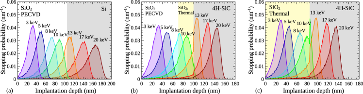
An overview of the investigated samples for this LE-SR study is given in Tables 1 and 2. A SiO2 film was formed on all samples, either by a low-temperature deposition in a PECVD chamber or by thermal growth in O2 ambient. As the focus of this study was the investigation of interface defects and their effect on the LE-SR signal, no post-oxidation annealing treatment was performed for any of the samples. The stopping profiles of the muons are simulated for each sample using the TRIMSP code,28, 29 and provide the mean stopping depth of the muon beam for a given implantation energy. The stopping profiles are calculated based on the measured densities of the two oxides and are presented for three of the samples in Figure 1. For muon implantation energies , the oxide layer is probed, while energies mainly probe the semiconductor bulk. In order to study the interface and near-interface region, implantation energies between these two values are used.
In SR, the so-called dia- and paramagnetic decay asymmetries and are determined by the amplitudes of the muon spin precession signals in an applied magnetic field transverse to the initial muon spin direction (transverse-field TF-SR). These asymmetries are proportional to the fraction of muons in the particular state. The respective fractions are calculated as: =/Atotal, and =2/Atotal, where Atotal is the maximally observable decay asymmetry of the SR spectrometer. The factor of 2 in results from the fact that only of the total Mu0 polarization is observable in our experiment with an applied magnetic field of .11 If no Mu0 is formed, the diamagnetic fraction is one. Smaller values - normally observed in insulators and semiconductors - indicate the formation of Mu0. At low temperatures and moderate doping of the semiconductor, more than of the implanted are expected to form such a paramagnetic state in Si or 4H-SiC.30, 25 Very often, some fraction of Mu0 states formed in insulators or semiconductors does not contribute to the precession signal due to fast muon spin depolarization processes, leading to a reduction of and to the observation, that, in general, + (which is called the missing fraction of muon spin polarization in SR).
The depth dependence of () and () was obtained from the correlation between implantation energy of the muon and mean stopping depth illustrated by the stopping profiles, with the fitting procedure detailed in Section 4. The simple model assumes and to be constant within each layer, and changing abruptly at the interface of two layers. As will be discussed below, for the deposited SiO2 samples, the fit result is consistent with the the measured thickness of the oxide, highlighting the accuracy of the analysis.
| Name | Crystal Orientation | ND () | Oxidation Process | tOx () |
|---|---|---|---|---|
| Si-A | (100) | PECVD | 105 | |
| Si-B | (100) | thermal | 110 | |
| Si-C | (100) | thermal, HF, PECVD | 95 |
2.1 The SiO2/Si Interface
The results of the LE-SR measurements (()) at for the SiO2/Si interface are summarized in Figure 2 (a-c) and corresponding fit results () are shown in Figure 2 (d-f). The vertical dotted lines represent the uncertainty in determining the exact interface position by profilometer and X-ray reflectivity measurements. Additionally, for Si-A and Si-B, was extracted from the measurements and are shown in Figure 2 (g-h).
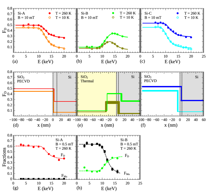
In SiO2, typically more than of the muons form Mu0, and almost of the implanted muons decay in the diamagnetic state.31, 32, 33 In PECVD-grown SiO2 (Figure 2 (a)), the diamagnetic fraction is about , possibly due to electron trapping in the low quality oxide, as hinted by the suppression of Mu0 formation (Figure 2 (g)).27, 24 In the case of the thermally grown oxide shown in Fig. 2 (b), the diamagnetic fraction for low implantation energies is significantly lower than for the deposited oxide and comparable to what was previously reported for SiO2 crystal or glass.32 Measurements performed with an externally applied magnetic field of , where the Mu0 procession signal can be directly observed, show a of (Figure 2 (h)), suggesting a higher structural order of SiO2 and hence an undisturbed Mu0 formation process in the SiO2 bulk.
Another remarkable difference is the effect each oxidation process has on the interface formed with the semiconductor. The PECVD-SiO2, deposited at low temperatures, can be clearly distinguished from Si in the SR signal, as quickly drops to the Si layer value at the interface (Figure 2 (d,f)). On the other hand, for sample Si-B with a thermally grown oxide, increases around the SiO2/Si interface, suggesting a defect-rich region or a region with higher structural disorder mainly on the SiO2 side ( ), but also on the Si side () of the interface. On the Si side, besides the presence of defects or structural disorder, the increase of could be also generated by electron accumulation in the interface region.18 In SiO2, the existence of a defect-rich region is further supported by the fitting results (in Figure 2 (h)) where a conversion of Mu0 to the diamagnetic state occurs at a muon implantation energy of , corresponding to a probing depth of away from the interface towards the oxide side. Thermal oxidation of Si is known to result in a large number of point-like defects in the SiO2 (E’ centers) and dangling bonds (Pb centers) at the interface.6, 7 These defects with energy levels in the bandgap can serve as traps for carriers and hence explain the observed differences of the diamagnetic signal between samples Si-A and Si-B. Furthermore, the growth of a thermal oxide on Si was previously shown to introduce stress into the interface system,34 resulting in a stress component both in the oxide, as well as in a narrow region in the Si.35 Although the oxidation-induced strain is expected to quickly relax away from the interface, stress-related lattice distortion may contribute to the observed reduction of in Figure 2 (h). However, in our samples, this strain-induced reduction of cannot be separated from the fast depolarization of Mu0 in Si due to the presence of free electrons/dopants with ND = ,14 as the detection of strain-induced effects on would require a Si sample with N to significantly reduce the dopant-induced depolarization of Mu0.
When removing the thermally grown SiO2 from the Si sample and depositing a PECVD-SiO2 instead (Figure 2 (c)), the defective region around the interface disappears and a very similar as for sample Si-A is observed. Interestingly, without the thermal oxide, the on the Si side also recovers to the same values as for the deposited oxide, suggesting that the Si is not permanently altered by the thermal oxidation.
At energies where the Si bulk is probed, all three samples show similar diamagnetic fractions of and for temperatures T = , respectively, indicating that the Si remains unchanged from the oxidation process at these depths. The larger value of at T = is a result of the thermally activated ionization of one of the two Mu0 states in Si: Mu0 can either form at the bond-center between two Si atoms (MuBC), or at the tetrahedral interstitial site (MuT).14, 30 It is the MuBC state with a fraction of which ionizes at T to form the diamagnetic Mu state 30, 36, 37 that can be observed in TF-SR at .
2.1.1 Electrical characterization of the SiO2
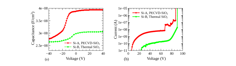
SiO2 layers formed by thermal oxidation or chemical vapor deposition are known to yield oxides with very different physical and electrical properties which is clearly reflected in the SR measurements. In order to connect our microscopic analysis to macroscopic device properties, an electrical analysis of metal-oxide-semiconductor (MOS) capacitors fabricated on the Si samples was performed. Capacitance-voltage (C-V) and current-voltage (I-V) measurements of the MOS capacitors are presented in Figure 3.
Despite the similar physical thickness of the two oxide layers, the C-V analysis reveals a much larger oxide capacitance for the deposited SiO2 () compared to the thermally grown film
(). This behavior may be explained by a larger water content for the deposited SiO2, causing an increase of the dielectric constant () from = for the thermally grown oxide to = for the PECVD-SiO2.38, 39 Extraction of the interface defect density ,40 reveals fairly large values for the thermally grown oxide ( = ) and the deposited oxide
( = ) which is expected for oxidation processes without any further annealing treatments. However, this also implies that the observed increase of around the interface of the thermally grown oxide (Si-B) can not solely be explained by the presence of dangling bonds at the SiO2/Si interface. Instead, one should consider a combination of factors, including oxide charges and interface traps in the SiO2 and at the interface, point defect and charge accumulation in the Si as well as strain-induced lattice distortions across the interface.
Differences between the two oxides are also observed in the breakdown measurements shown in Figure 3 (b), where the porous PECVD-SiO2 shows almost two orders of magnitude higher leakage currents and an earlier breakdown compared to the thermally grown SiO2.
2.2 The SiO2/4H-SiC Interface
| Name | Crystal Orientation | ND () | Oxidation Process | tOx () |
|---|---|---|---|---|
| SiC-A | (0001)Si | PECVD | 105 | |
| SiC-B | (0001)Si | thermal + PECVD | 30 + 70 | |
| SiC-C | (000)C | thermal | 90 | |
| SiC-D | (000)C | thermal, HF, PECVD | 95 |
Unlike for the Si samples where we mainly discussed the muon response to different SiO2 films, in the case of the SiC samples we also studied how the doping concentration of the semiconductor impacts the and formation process across the interface. A summary of the processing parameters of the SiC samples is given in Table 2. While the SiO2/SiC interface was formed on the low-doped (0001) Si-face for samples SiC-A and SiC-B, measurements on samples SiC-C and SiC-D were performed on the highly doped (000) C-face. As the oxide growth rate at for (0001) 4H-SiC is too low to achieve the targeted oxide thickness of , only a -thick oxide was thermally grown on sample SiC-B and a -thick PECVD-SiO2 was deposited on top. In order to investigate any permanent change of the SiC due to thermal oxidation, sample SiC-D was first thermally oxidized before the oxide layer was removed again and a PECVD-SiO2 was deposited instead.
Figure 4 (a-c) and 5 (a) show measured on the 4H-SiC samples with an applied magnetic field of , measurements performed at are presented in Figure 4 (g-i). Again, the vertical dotted lines represent the uncertainty in determining the exact interface position by profilometer and X-ray reflectivity measurements.
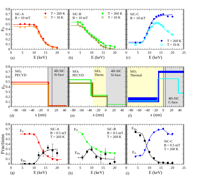
As shown before for the Si samples, the depth-dependence of () in Figure 4 (d-e) clearly indicates the SiO2/SiC interface where quickly drops to the typical 4H-SiC bulk value.24, 25
The PECVD oxide of samples SiC-A, SiC-B, and SiC-D shows a similar behavior as on Si with a strong increase of compared to the bulk SiC and a suppression of Mu0 formation across the whole oxide layer. Similarly to Si-B, the thermal oxide in the SiC-B and SiC-C samples has a higher structural order compared to PECVD-SiO2, allowing observation of the Mu0 precession in the SiO2 layers.
Thermal oxidation of Si and SiC is very similar, however, in the case of SiC, it does not only involve the formation of bonds between Si and O, but also removal of C through the oxide. If the carbon atoms are not efficiently removed from the interface, they may form carbon-related defects directly at, or in the vicinity of the SiO2/SiC interface. Hence, apart from dangling bonds, interfacial carbon clusters and near-interface oxide traps are expected to contribute to the interface defect state density.41 Additionally, electrically detected magnetic resonance (EDMR) measurements also suggest the out-diffusion of Si from the SiC bulk and the generation of silicon vacancies as a source for the increased defect concentrations close to the SiO2/SiC interface.42, 43 The Si-out diffusion during thermal oxidation, leads to a C-rich surface where large areas of graphene-like mono-layers are likely to form. 44 For the SiC samples discussed here, the analysis revealed a larger interface defect density ( = ) for the thermally grown oxide (SiC-B) compared to the Si samples or the deposited SiO2 on sample SiC-A ( = ). The effect of enhanced defect concentrations in the thermally grown SiO2 layer correlates with the observed increase of in the narrow thick thermal-SiO2 layer in SiC-B. Although Mu0 is visible in the thermal-SiO2 layer of SiC-B (figure 4 (h)), the enhanced of in Figure 4 (e) is comparable to the value measured at in the defective SiO2 region near the interface of Si-B (Figure 2 (e)). Thus, in SiC-B the layer of thermally grown SiO2 seems to be affected by defects and oxidation-induced stress, which is reported to be more pronounced across the SiO2/SiC interface than that of SiO2/Si,45 and also appears broader than the oxide defective region in Si-B and SiC-C.
The quality of the oxide near the interface formed with SiC also depends on the polarity of the oxidized SiC face. The thermal oxidation process is almost ten times faster for the C-face of SiC than for the Si-face.46 Therefore, the resulting oxide thickness using the same process parameters as for SiC-A and SiC-B results in a thermal-SiO2 layer on the C-face in SiC-C. A region with enhanced formation, like in Si-B, appears near the interface. The oxide defective region in SiC-C is narrower than in SiC-B, and affects only (Figure 4 (f)), which suggests less induced strain for SiO2 layers on the C-face.47 However, the higher for SiC-C, compared to Si-B and SiC-B, suggests the presence of a much higher for SiO2 grown on C-face.48, 49 The extension of the region with enhanced formation into SiC also differs between Si- and C-face samples: it is in SiC-B, much narrower compared to the in SiC-C and SiC-D. The graphitization of SiC is considered to strongly contribute to the observations since in Si-face SiC only mono-layers of graphene are expected to form at , whereas the C-face graphitizes at lower temperatures and generates three-dimensional layers. 50, 51 Thus, the wide region with a sharp rise in observed in C-face SiC-C and SiC-D is likely related to the formation of a graphene-like layer in SiC near the interface. However, this difference cannot be solely attributed to the impact of crystal orientation on the oxidation process, as it is indistinguishable from the effect of different doping concentrations on at the surfaces of the semiconductors, where SiC-B has a three orders of magnitude smaller doping concentration than SiC-C.
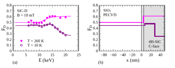
In SiC-A, is nearly temperature-independent (Figure 4 (a,d)) in the SiC crystal where the Mu0 signal is visible, and the respective fractions in Figure 4 (g) are comparable to similarly doped epitaxial SiC reported by Woerle et al.24, 25 Although the doping concentration of SiC-B is the same as of SiC-A, the thermal oxidation in SiC-B leads to an unexpected increase of to 20% within the semiconductor at (Figure 4 (h)). Defects related to the carbon vacancy in SiC have been shown to lead to an increased , while a paramagnetic fraction of still remains.24 However, it is unlikely that carbon vacancies are responsible for the observations in Figure 4 (h), since the oxidation process itself is initiated by a Si out-diffusion and only a later destruction of the C sub-lattice.52 Furthermore, LE-SR is only sensitive to carbon defect concentrations , where Mu0 still can be observed. In contrast, the Mu0 signal disappears in the SiC layer of the SiC-B sample. Such a disappearance of the Mu0 signal can be explained by the interaction with free charge carriers, and formation of a diamagnetic state. The increase of is hardly observable at , which suggests that there is a neutral Mu0 precursor state which quickly dephases.24 At , due to the smaller precession frequencies of the muon spin in Mu0 compared to , the contribution of either electron or hole capture by Mu0 to form Mu- or Mu+, respectively, can be observed. An accumulation of holes near the SiC surface would be in agreement with the reports of energy band structure of SiO2/SiC, which promotes depletion of electrons at the SiC interface.53 Therefore it is likely that the increase at is due to delayed formation of Mu+, favoured by the band-bending caused by thermal oxidation of the Si-face SiC.
The high value of at in a 30-nm-wide region inside the semiconductor in highly-doped, C-face SiC-C and SiC-D hints towards an electron-rich region near the interface. The graphene layer grown on SiC has been reported to be n-type. 54 The doping is proposed to originate from three different mechanisms, which at times coexist: electron transfer from interface states (Si and C dangling bonds) to the graphene layer, polarization induced by the hexagonal geometry of the 4H-SiC substrate, and the effect of a space-charge region in doped SiC. Additionally, electron exchange with the bulk is also compatible with the C-face SiC substrate doping concentration of . 55, 56, 57 At a distance beyond from the interface, drops to . It is obvious to assume that the formation of this diamagnetic fraction in the ”bulk” of the SiC originates from the capture of majority charge carriers (electrons) of Mu0. Comparing with unpublished data where we measured for various n- and p-doping levels up to , a fraction of corresponds to an electron concentration of . This is much smaller than the bulk doping level of , since at 10 K, only a small fraction of donors is ionized. The increase of to closer to the interface would then mean an increase of to in the 30-nm-wide region of C-face SiC. Although an increase of could also be sustained by hole capture of Mu0 to form Mu+, the minority charge carrier concentration required to obtain = would have to be about five times larger than the estimated above, because the hole capture rate of Mu0 is governed by the hole mobility, 58 which is about five times lower in 4H-SiC than the electron mobility. This would require a hole carrier concentration , which is larger than the n-type doping concentration. Therefore, the remarkable increase of in the highly doped C-face SiC, at the expense of Mu0 (Figure 4 (f)), can be attributed to an enhanced concentration of electrons, in the n-type layer at the surface of SiC, leading to an increased Mu- formation probability. Considering the previously discussed defect formation mechanisms during thermal oxidation, the change in carrier concentration can be attributed to the negatively charged graphene-like layer near the interface of the oxidized C-face.
An interesting memory effect is observed in SiC-D at (Figure 5), where the thermal oxide was replaced by a deposited oxide. A region with high is still present in C-face SiC even after removing the thermally grown SiO2, suggesting that the oxidation process caused a permanent modification of the SiC crystal, e.g. by emission of oxidation by-products into the SiC crystal. Interestingly, only increases a few nanometers below the SiO2/SiC interface, suggesting a narrow C-rich layer, as discussed for SiC-C, which was not removed during HF etching,59 and is still present below the PECVD oxide.
In SiC-C and SiC-D, conversion of to is visible in the semiconductor at ((Figure 4 (i)), as the thermal ionization of nitrogen donors takes place at T , where the availability of free electrons from the ionized donors promote the formation of Mu- from Mu0 precursor states. Thus, at the n-type C-rich region where is enhanced is no longer distinguishable due to the high concentration of free electrons. This enhanced Mu- formation at 260 K is the cause for the higher value of 70% deep ( 40 nm) inside the semiconductor, compared to 25% at 10 K.
3 Conclusion
In this study, we have demonstrated our recent progress on low-energy muon spin rotation for the investigation of oxide-semiconductor interfaces. LE-SR offers a depth-resolved analysis of interfacial systems without the need for dedicated device structures or sophisticated system models for the interpretation of the data. The muon’s sensitivity to defects and charge carriers allowed to distinguish characteristic properties of PECVD SiO2 and thermally grown SiO2 and their effect on the semiconductors: the high-temperature oxidation of Si and SiC results in an oxide with a superior structural order where the atom-like Mu0 is likely to form, whereas in a PECVD-SiO2 deposited at only a large is observable. The samples with PECVD-SiO2 exhibit an abrupt transition from the oxide to the semiconductor, whereas samples with thermally grown SiO2 exhibit a wide region with enhanced in the oxide near the interface. In the case of Si, the region with increased at the interface inside the semiconductor disappeared once the thermal oxide was etched back and a PECVD-SiO2 layer was deposited instead. In SiC, both the width of the region with enhanced , and the strength of the diamagnetic signal induced by the thermal oxidation were shown to depend on the crystal orientation. In the C-face SiC samples, the region extends into the semiconductor and is still visible after etching the thermal oxide and deposition of PECVD-SiO2. The increase in on the SiO2 side of the interface is attributed to a combination of factors such as interface defects, near-interface oxide traps, and oxidation-induced stress. On the SiC side of the interface, the higher in the first tens of nanometers is a result of the sensitivity of the SR signal to a change in charge carrier concentration at the SiC surface. These changes depend on the corresponding bulk carrier concentration and the overall oxidation process: on the Si-face depletion of electrons and hole capture sustains Mu+ formation, and on the C-face, Mu- forms in the C-rich n-type layer.
These results demonstrate that LE-SR has the potential to deliver information about structural and electronic properties of oxide-semiconductor interfaces with hitherto inaccessible sensitivity and depth resolution. A good understanding of interface properties is critical for device operation, and the information provided by LE-SR can, in turn, advance the development of reliable SiC power devices.
4 Experimental Section
Sample preparation
For this experiment, (100) silicon with a nitrogen donor concentration of = as well as (0001) Si-face 4H-SiC ( = ) and (000) C-face 4H-SiC ( ) were used. All samples were cut into sizes of and wet-chemically cleaned prior to oxidation. The oxide was either thermally grown at in O2 ambient or deposited at in a PECVD chamber. No post-oxidation annealing or other processes for improving the oxide quality were performed for any of the samples. The final oxide thicknesses were confirmed by profilometer and reflectometer measurements. Two samples, Si-C and SiC-D, were first thermally oxidized before the SiO2 was removed again by dipping the sample in hydrofluoric acid (HF) and another SiO2 layer was deposited on the samples. As the oxide growth rate at is very low on the (0001) Si-face of 4H-SiC, only a -thick oxide was thermally grown on sample SiC-B and another SiO2 layer of was deposited on top.
Density measurements
Additional X-ray reflectivity (XRR) measurements proved helpful for the estimation of oxide densities: for thermally grown oxides, a density of = was extracted, whereas the deposited oxide had a slightly smaller density of = .
Electrical characterization
After the SR experiment, MOS structures were fabricated on the samples and C-V and current-voltage (I-V) measurements were performed. The values were determined from the capacitance and conductance curves obtained at .
SR measurements
The LE-SR experiments were performed at the low-energy muon facility (LEM) located at the E4 beamline60 of the Swiss Muon Source (SS, Paul Scherrer Institute, Villigen, Switzerland).
The samples were glued with conductive silver paint onto a Ni-coated aluminum sample plate, mounted on a cold-finger cryostat.
The muon implantation energy ranged from , probing the first of the SiC and Si samples, respectively. The energy dependent measurements were carried out at temperatures of , with transverse magnetic fields of applied parallel to the beam axis. At a magnetic field of only the diamagnetic signal can be resolved due to the frequency detection limit of of the instrument. Additionally, at the precession signal of Mu0 is detected, where only about of the total polarization is visible.11 For measurements 3 million low-energy muon events were recorded, and 8 million events for measurements.
The SR asymmetry spectra were analyzed using the software musrfit.61 At a field of , where in our case only the diamagnetic signal with asymmetry is observable, an exponentially-damped cosine function at the Larmor frequency of the muon was used to fit the data
| (1) |
where is the depolarization rate of the diamagnetic state, and is the phase of the precession signal in a specific positron detector. At , a second component becomes visible, which is the precession of the paramagnetic Mu0 state with asymmetry :
| (2) |
where is the exponential depolarization rate of Mu0, is the muon spin precession frequency in the Mu0 triplet state,11 and it is assumed that the diamagnetic and paramagnetic components have the same detector phase .
In 4H-SiC, the Mu0 precession frequency splits into two lines due to a so far unreported weak anisotropy of the hyperfine coupling of on top of the isotropic part with a much larger coupling of about :
| (3) |
where , and , see Fig. 6. The isotropic coupling has been determined in Ref. 62, where the authors indicated the presence of a presumably small anisotropic component in the hyperfine coupling. In the analysis of our data, the splitting of the Mu0 lines in 4H-SiC allows to distinguish the fractions of muonium forming in the oxide and in SiC.
SR fitting procedure
The method implemented by Simões et al. takes advantage of the nanometer depth-resolution of the LE-SR technique to infer the depth variation of the parameters from the experimentally measured energy dependence.63
In this work, the depth dependence of the diamagnetic fraction is obtained using the correlation of the muon implantation energy and its stopping depth, the stopping probability (,), calculated via the Monte Carlo simulation TRIMSP 28, 29 for all the samples. (,) is the probability per unit length that a muon implanted with energy stops in the material at a depth , as shown for different samples in Figure 1.
The fraction of muons with a final diamagnetic state depends on the material, and has distinct characteristic values for the oxide and the semiconductor. Thus, we assume a step-like function to be a good approximation of the variation within the structure.17, 64
Acknowledgements
The muon measurements have been performed at the Swiss Muon Source SS, Paul Scherrer Institute, Villigen, Switzerland. We thank Dr. Laura Maurel Velàzquez for performing the XRR measurements.
References
- [1] W. J. Choyke, G. Pensl, MRS Bulletin 1997, 22, 3 25.
- [2] S. E. Saddow, Micromachines 2022, 13, 3.
- [3] N. T. Son, C. P. Anderson, A. Bourassa, K. C. Miao, C. Babin, M. Widmann, M. Niethammer, J. Ul Hassan, N. Morioka, I. G. Ivanov, F. Kaiser, J. Wrachtrup, D. D. Awschalom, Applied Physics Letters 2020, 116, 19 190501.
- [4] M. E. Bathen, L. Vines, Advanced Quantum Technologies 2021, 4, 7 2100003.
- [5] S. M. Sze, K. K. Ng, Physics of Semiconductor Devices, Wiley, 2007.
- [6] D. K. Schroder, Semiconductor Material and Device Characterization, John Wiley & Sons, Inc., 2005.
- [7] S. Kasap, P. Capper, editors, Springer Handbook of Electronic and Photonic Materials, Springer, 2017.
- [8] B. Hornetz, H.-J. Michel, J. Halbritter, Journal of Materials Research 1994, 9, 12 3088.
- [9] J. A. Taillon, J. H. Yang, C. A. Ahyi, J. Rozen, J. R. Williams, L. C. Feldman, T. S. Zheleva, A. J. Lelis, L. G. Salamanca-Riba, Journal of Applied Physics 2013, 113, 4 044517.
- [10] T. L. Biggerstaff, C. L. Reynolds, T. Zheleva, A. Lelis, D. Habersat, S. Haney, S.-H. Ryu, A. Agarwal, G. Duscher, Applied Physics Letters 2009, 95.
- [11] Stephen J. Blundell, Roberto De Renzi, Tom Lancaster, Francis L. Pratt, editors, Muon Spectroscopy - An Introduction, Oxford University Press, Oxford, 2021.
- [12] A. D. Hillier, S. J. Blundell, I. McKenzie, I. Umegaki, L. Shu, J. A. Wright, T. Prokscha, F. Bert, K. Shimomura, A. Berlie, H. Alberto, I. Watanabe, Nature Reviews Methods Primers 2022, 2, 1 1.
- [13] P. W. Percival, Radiochimica Acta 1979, 26, 1 1.
- [14] B. D. Patterson, Reviews of Modern Physics 1988, 60, 1 69.
- [15] S. F. J. Cox, Reports on Progress in Physics 2009, 72, 11 116501.
- [16] D. G. Eshchenko, V. G. Storchak, J. H. Brewer, G. D. Morris, S. P. Cottrell, S. F. J. Cox, Physical Review B 2002, 66, 3 035105.
- [17] H. V. Alberto, R. C. Vilão, R. B. L. Vieira, J. M. Gil, A. Weidinger, M. G. Sousa, J. P. Teixeira, A. F. da Cunha, J. P. Leitão, P. M. P. Salomé, P. A. Fernandes, T. Törndahl, T. Prokscha, A. Suter, Z. Salman, Phys. Rev. Materials 2018, 2 025402.
- [18] T. Prokscha, K.-H. Chow, Z. Salman, E. Stilp, A. Suter, Phys. Rev. Applied 2020, 14 014098.
- [19] E. Morenzoni, T. Prokscha, A. Suter, H. Luetkens, R. Khasanov, Journal of Physics: Condensed Matter 2004, 16, 40 4583.
- [20] D. R. Harshman, A. P. Mills, J. L. Beveridge, K. R. Kendall, G. D. Morris, M. Senba, J. B. Warren, A. S. Rupaal, J. H. Turner, Rapid Communications 1987, 36, 16 8850.
- [21] E. Morenzoni, F. Kottmann, D. Maden, B. Matthias, M. Meyberg, T. Prokscha, T. Wutzke, U. Zimmermann, Physical Review Letters 1994, 72, 17.
- [22] E. Morenzoni, H. Glückler, T. Prokscha, H. P. Weber, E. M. Forgan, T. J. Jackson, H. Luetkens, C. Niedermayer, M. Pleines, M. Birke, A. Hofer, J. Litterst, T. Riseman, G. Schatz, Physica B: Condensed Matter 2000, 289-290 653.
- [23] T. Prokscha, E. Morenzoni, C. David, A. Hofer, H. Glückler, L. Scandella, Applied Surface Science 2001, 172 235.
- [24] J. Woerle, T. Prokscha, A. Hallén, U. Grossner, Physical Review B 2019, 100, 11 115202.
- [25] J. Woerle, M. E. Bathen, T. Prokscha, A. Galeckas, H. M. Ayedh, L. Vines, U. Grossner, Physical Review Applied 2020, 14, 5.
- [26] T. Prokscha, K. H. Chow, E. Stilp, A. Suter, H. Luetkens, E. Morenzoni, G. J. Nieuwenhuys, Z. Salman, R. Scheuermann, Scientific reports 2013, 3, 1 1.
- [27] T. Prokscha, H. Luetkens, E. Morenzoni, G. J. Nieuwenhuys, A. Suter, M. Döbeli, M. Horisberger, E. Pomjakushina, Physical Review B 2014, 90, 23 235303.
- [28] W. Eckstein, Computer Simulation of Ion-Solid Interactions, Springer Series in Materials Science. Springer Berlin Heidelberg, 1991.
- [29] E. Morenzoni, H. Glückler, T. Prokscha, R. Khasanov, H. Luetkens, M. Birke, E. M. Forgan, C. Niedermayer, M. Pleines, Nuclear Instruments and Methods in Physics Research Section B: Beam Interactions with Materials and Atoms 2002, 192, 3 254.
- [30] S. R. Kreitzman, B. Hitti, R. L. Lichti, T. L. Estle, K. H. Chow, Physical Review B 1995, 51, 19 13117.
- [31] R. F. Kiefl, J. B. Warren, C. J. Oram, G. M. Marshall, J. H. Brewer, D. R. Harshman, C. W. Clawson, Physical Review B 1982, 26, 5 2432.
- [32] T. Prokscha, E. Morenzoni, D. G. Eshchenko, N. Garifianov, H. Glückler, R. Khasanov, H. Luetkens, A. Suter, Physical Review Letters 2007, 98, 22 227401.
- [33] N. Funamori, K. M. Kojima, D. Wakabayashi, T. Sato, T. Taniguchi, N. Nishiyama, T. Irifune, D. Tomono, T. Matsuzaki, M. Miyazaki, M. Hiraishi, A. Koda, R. Kadono, Scientific Reports 2015, 5.
- [34] K. Queeney, M. Weldon, J. Chang, Y. Chabal, A. Gurevich, J. Sapjeta, R. Opila, Journal of Applied Physics 2000, 87, 3 1322.
- [35] E. Kobeda, E. Irene, Journal of Vacuum Science & Technology B: Microelectronics Processing and Phenomena 1987, 5, 1 15.
- [36] I. Fan, K. H. Chow, B. Hitti, R. Scheuermann, W. A. MacFarlane, A. I. Mansour, B. E. Schultz, M. Egilmez, J. Jung, R. L. Lichti, Physical Review B 2008, 77, 3 035203.
- [37] T. Prokscha, Physics Procedia 2012, 30 50.
- [38] C. Pavelescu, J. P. McVittie, C. Chang, K. C. Saraswat, J. Y. Leong, Thin Solid Films 1992, 217, 1-2 68.
- [39] I. Idris, O. Sugiura, Japanese Journal of Applied Physics 1998, 37, Part 1, No. 12A 6562.
- [40] E. H. Nicollian, J. R. Brews, MOS Physics and Technology, Wiley-Interscience, 1982.
- [41] S. Dhar, S. T. Pantelides, J. R. Williams, L. C. Feldman, In D. M. Fleetwood, R. D. Schrimpf, editors, Defects in Microelectronic Materials and Devices, chapter 20. CRC Academic Press, 2009.
- [42] C. J. Cochrane, P. M. Lenahan, A. J. Lelis, Journal of Applied Physics 2011, 109, 1 014506.
- [43] M. A. Anders, P. M. Lenahan, C. J. Cochrane, A. J. Lelis, IEEE Transactions on Electron Devices 2015, 62, 2 301.
- [44] J. Hass, W. De Heer, E. Conrad, Journal of Physics: Condensed Matter 2008, 20, 32 323202.
- [45] M. Yoshikawa, Y. Fujita, M. Murakami, Applied spectroscopy 2019, 73, 10 1193.
- [46] Y. Song, S. Dhar, L. C. Feldman, G. Chung, J. R. Williams, Journal of Applied Physics 2004, 95, 9 4953.
- [47] H. Hirai, K. Kita, Applied Physics Letters 2017, 110, 15 152104.
- [48] V. V. Afanas’ev, M. Bassler, G. Pensl, M. J. Schulz, Phys. Stat. Sol. (a) 1997, 162.
- [49] K. Fukuda, W. Cho, K. Arai, S. Suzuki, J. Senzaki, T. Tanaka, Applied Physics Letters 2000, 77, 6 866.
- [50] Luxmi, N. Srivastava, G. He, R. M. Feenstra, P. J. Fisher, Phys. Rev. B 2010, 82 235406.
- [51] N. Srivastava, G. He, Luxmi, P. C. Mende, R. M. Feenstra, Y. Sun, Journal of Physics D: Applied Physics 2012, 45, 15 154001.
- [52] J. Woerle, B. C. Johnson, C. Bongiorno, K. Yamasue, G. Ferro, D. Dutta, T. A. Jung, H. Sigg, Y. Cho, U. Grossner, M. Camarda, Physical Review Materials 2019, 3, 8.
- [53] H. Watanabe, T. Kirino, Y. Kagei, J. Harries, A. Yoshigoe, Y. Teraoka, S. Mitani, Y. Nakano, T. Nakamura, T. Hosoi, et al., In Materials Science Forum, volume 679. Trans Tech Publ, 2011 386–389.
- [54] S. Kopylov, A. Tzalenchuk, S. Kubatkin, V. I. Fal’ko, Applied Physics Letters 2010, 97, 11 112109.
- [55] J. Ristein, S. Mammadov, T. Seyller, Phys. Rev. Lett. 2012, 108 246104.
- [56] S. Mammadov, J. Ristein, R. J. Koch, M. Ostler, C. Raidel, M. Wanke, R. Vasiliauskas, R. Yakimova, T. Seyller, 2D Materials 2014, 1, 3 035003.
- [57] A. Pradeepkumar, D. K. Gaskill, F. Iacopi, Applied Sciences 2020, 10, 12.
- [58] T. Prokscha, Journal of Physics: Conference Series 2014, 551 012049.
- [59] B. C. Johnson, J. Woerle, D. Haasmann, C. T.-K. Lew, R. A. Parker, H. Knowles, B. Pingault, M. Atature, A. Gali, S. Dimitrijev, M. Camarda, J. C. McCallum, Physical Review Applied 2019, 12, 4, in Review.
- [60] T. Prokscha, E. Morenzoni, K. Deiters, F. Foroughi, D. George, R. Kobler, A. Suter, V. Vrankovic, Nuclear Instruments and Methods in Physics Research Section A: Accelerators, Spectrometers, Detectors and Associated Equipment 2008, 595, 2 317.
- [61] A. Suter, B. Wojek, Physics Procedia 2012, 30 69.
- [62] R. L. Lichti, W. A. Nussbaum, K. H. Chow, Physical Review B 2004, 70, 16 165204.
- [63] A. F. A. Simões, H. V. Alberto, R. C. Vilão, J. M. Gil, J. M. V. Cunha, M. A. Curado, P. M. P. Salomé, T. Prokscha, A. Suter, Z. Salman, Review of Scientific Instruments 2020, 91, 2 023906.
- [64] M. Curado, J. Teixeira, M. Monteiro, E. Ribeiro, R. Vilão, H. Alberto, J. Cunha, T. Lopes, K. Oliveira, O. Donzel-Gargand, A. Hultqvist, S. Calderon, M. Barreiros, W. Chiappim, J. Leitão, A. Silva, T. Prokscha, C. Vinhais, P. Fernandes, P. Salomé, Applied Materials Today 2020, 21 100867.