Hard superconducting gap in germanium
Abstract
The co-integration of spin, superconducting, and topological systems is emerging as an exciting pathway for scalable and high-fidelity quantum information technology. High-mobility planar germanium is a front-runner semiconductor for building quantum processors with spin-qubits, but progress with hybrid superconductor-semiconductor devices is hindered because obtaining a superconducting gap free of subgap states (hard gap) has proven difficult. Here we solve this challenge by developing a low-disorder, oxide-free interface between high-mobility planar germanium and a germanosilicide parent superconductor. This superconducting contact is formed by the thermally-activated solid phase reaction between a metal (Pt) and the semiconductor heterostructure (Ge/SiGe). Electrical characterization reveals near-unity transparency in Josephson junctions and, importantly, a hard induced superconducting gap in quantum point contacts. Furthermore, we demonstrate phase control of a Josephson junction and study transport in a gated two-dimensional superconductor–semiconductor array towards scalable architectures. These results expand the quantum technology toolbox in germanium and provide new avenues for exploring monolithic superconductor-semiconductor quantum circuits towards scalable quantum information processing.
The intimate coupling between superconductors and semiconductors in hybrid devices is at the heart of exciting pursuits, including topological qubits with Majorana zero modes Lutchyn et al. (2018); Flensberg et al. (2021), superconducting (Andreev) spin qubits Hays et al. (2021), and gate-tunable superconducting qubits Casparis et al. (2018). Combining hybrid devices with high-fidelity semiconductor spin qubits in a single material platform may resolve key challenges for scalable quantum information processing. In particular, quantum information transfer between spin and topological qubits Choi et al. (2000); Leijnse and Flensberg (2011, 2012); Hoffman et al. (2016) may enable a universal gate set for topological quantum computation and, conversely, superconductors may be used to coherently couple spin qubits at a distance via crossed Andreev reflection Choi et al. (2000); Leijnse and Flensberg (2013) or topologically protected links Kitaev (2001).
The use of epitaxial superconducting Al to induce a hard superconducting gap in III-V semiconductors Chang et al. (2015); Kjaergaard et al. (2016) stimulated great progress with hybrid devices, leading to experimental reports of topological superconductivity in planar Josephson junctions Fornieri et al. (2019a) and in electrostatically defined quasi-1D wires Aghaee et al. (2022), the demonstration of Andreev spin qubits Hays et al. (2021), and the realization of a minimal Kitaev chain in coupled quantum dots Dvir et al. (2022). However, spin qubits in III-V semiconductors suffer from the hyperfine interactions with the nuclear spin bath Cywiński et al. (2009) that severely deteriorate their quantum coherence Stano and Loss (2022) and challenges their integration with hybrid devices.
On the other hand, spin qubits with quantum dots in Ge Scappucci et al. (2020); Watzinger et al. (2018); Hendrickx et al. (2020); Jirovec et al. (2021) can achieve long quantum coherence due to the suppressed hyperfine interaction Prechtel et al. (2016) and the possibility of isotopic purification into a nuclear spin-free material Itoh and Watanabe (2014). Thanks to the light effective mass Lodari et al. (2019) and high mobility exceeding one million cm/Vs Lodari et al. (2022), holes in planar Ge/SiGe heterostructures have advanced semiconductors spin qubits to the universal operation on a qubit array Hendrickx et al. (2021), and the shared control of a 16 semiconductor quantum dot crossbar array Borsoi et al. (2022). Moreover, the ability of holes to make contacts with low Schottky barrier heights to metals Dimoulas et al. (2006), including superconductors, makes Ge a promising candidate for hybrid devices. Initial work used superconducting Al to contact Ge either via thermal diffusion Hendrickx et al. (2018, 2019); Ridderbos et al. (2019) or by deposition on the sidewalls of etched mesas Vigneau et al. (2019); Aggarwal et al. (2021). However, the key demonstration of a superconducting gap in Ge free of subgap quasiparticle states is lacking, challenged by the difficulty of contacting uniformly a buried quantum well with a superconductor, whilst maintaining the low disorder at the superconductor-semiconductor interface and in the semiconductor channel.
Here we solve these challenges and demonstrate a hard superconducting gap in Ge. We contact the quantum well with a superconducting germanosilicide (PtSiGe), similar to the silicidation process used by the microelectronics industry for low resistance contacts Kittl et al. (2008). The superconductor is formed uniformly within the heterostructure and reaches the buried quantum well via a controlled thermally-activated solid phase reaction between the metal (Pt) and the semiconductor stack (Ge/SiGe). This process is simple, robust, and does not require specialised vacuum conditions or etching because the superconductor-semiconductor interface is buried into the pure semiconducting heterostructure and consequently remains pristine. This represents a paradigm shift compared to the subtractive nanofabrication processes commonly used for hybrid devices, since our additive process does not deteriorate the active area of the semiconductor. As a result, we demonstrate a suite of reproducible Ge hybrid devices with low disorder and excellent superconducting properties.
.
.1 Material properties
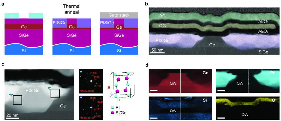
Our approach to superconductor-semiconductor hybrid devices in Ge is illustrated in Fig. Hard superconducting gap in germaniuma. We use an undoped and compressively-strained Ge quantum well, grown by chemical vapor deposition on a Si(001) wafer Sammak et al. (2019) and separated from the surface by a SiGe barrier (Methods). This heterostructure supports a two-dimensional hole gas (2DHG) with high mobility (), long transport scattering time (), and long mean free path () (Supplementary Fig. S1) and hosts high-performance spin-qubits Hendrickx et al. (2020). Crucial for the reliable search of topological superconductivity Ahn et al. (2021) and for scaling to large spin-qubit architectures Vandersypen et al. (2017), the disorder in our buried Ge quantum wells is characterised by an energy level broadening of meV, which is more than one order of magnitude smaller than in the other material systems exhibiting a hard superconducting gap (Supplementary Table S1).
As shown by the schematics in Fig. Hard superconducting gap in germaniuma, we obtain PtSiGe contacts to the quantum well by room-temperature evaporation of a Pt supply layer, metal lift-off, and rapid thermal process at (Methods). This low-temperature process preserves the structural integrity of the quantum well grown at , whilst activating the solid phase reaction driving Pt into the heterostructure and Ge and Si into the Pt (Supplementary Fig. S3). As a result, low-resistivity germanosilicide phases are formed Gaudet et al. (2006) and under these process conditions the obtained PtSiGe films are superconducting with a and an in-plane critical field of mT (Supplementary Fig. S2). Finally, we use patterned electrostatic gates, insulated by dielectric films in between, to accumulate charge carriers in the quantum well and to shape the electrostatic confinement potential of the hybrid superconductor-semiconductor devices (Methods). Because we do not perform any etch during the nanofabrication of hybrid devices, the low-disorder landscape that determines the 2DHG high mobility is likely to be preserved when further dimensional confinement is achieved by means of electrostatic gates. This is different for hybrid devices with III-V semiconductors, since etching of the superconductor in the active semiconductor region causes mobility degradation Shabani et al. (2016).
The morphological, structural, and chemical properties of the hybrid devices are inferred by aberration corrected (AC) high-angle annular dark-field scanning transmission electron microscopy (HAADF-STEM) and electron energy-loss spectroscopy (EELS). Fig. Hard superconducting gap in germaniumb shows a HAADF-STEM image of a cross-section of a superconductor-normal-superconductor quantum point contact (SNS-QPC) taken off-center to visualise the two gate layers (Fig 2a shows a top view of the device). We observe a uniform quantum well of high-crystalline quality, with sharp interfaces to the adjacent SiGe and absence of extended defects. As a result of the annealing, Pt diffuses predominantly vertically through the SiGe spacer reaching the quantum well. The sharp lateral interfaces between the two PtSiGe contacts and the QW in between set the length of the channel populated by holes via the top-gates. The PtSiGe film presents poly-crystalline domains with a crystal size up to 5050 nm and orthorhombic phase (PBNM, space group number 62) Alptekin et al. (2009). This is inferred from the power spectra or fast Fourier transforms (FFTs) taken from the two PtSiGe domains interfacing with the QW from the left contact, shown in Fig. Hard superconducting gap in germaniumc along with a schematic view of the unit cell of such phase. The analysis of EELS elemental concentration profiles across the Ge QWPtSiGe heterointerface (Supplementary Fig. S4) reveals that the threefold PtSiGe stoichiometry is Ge-rich, with relative composition in the range between and depending locally on the analysed grain. The EELS compositional maps in Fig. Hard superconducting gap in germaniumd show the elemental distribution of Ge, Si, Pt, Al, and O, at the key regions of the device. We observe Pt well confined to the two contacts areas, which also appear Ge-rich. Crucially, O is detected only in the AlO dielectric layer below the gates, pointing to a high-purity quantum well and a pristine superconductor-semiconductor interface.
.2 Highly transparent Josephson junction
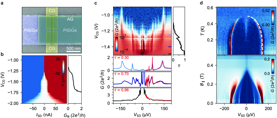
We perform low-frequency four-terminal current and voltage bias measurements (Methods) on the SNS-QPC device shown in Fig. 2a to infer the properties of the superconductor-semiconductor interface. Accumulation (AC, in green) and constriction (CG, in yellow) gates control transport within the 70 nm long channel between the two PtSiGe leads. We apply a large negative voltage to the accumulation gate to populate the quantum well with holes, and we then control the effective width of the channel by applying a more positive voltage to the constriction gates, thus depleting the underlying quantum well.
The current bias measurements (Fig. 2b) reveal a tunable supercurrent with a plateau when the constriction gate voltage is in the range V. This is the same range where we observe the first conductance plateau in the normal-state conductance (Fig. 2b, right inset), indicating that the switching current () plateau observed in the color plot stems form the supercurrent discretization due to the discrete number of modes in the QPC Hendrickx et al. (2019); Irie et al. (2014). Supercurrent discretization up to the third conductance plateau is shown in Supplementary Fig. S5 (data are for a different SNS-QPC device with identical design to the one presented here). We use the switching current as a lower bound for the critical current and we estimate an product of , showing an improvement as compared to previous results obtained with pure Al contacts in Ge QWs Hendrickx et al. (2019); Vigneau et al. (2019); Aggarwal et al. (2021), despite the Al is higher than the PtSiGe . The measured product is the theoretical product calculated for a ballistic short junction using the Ambegaokar–Baratoff formula with being the critical current, the induced superconducting gap and the electron charge Ambegaokar and Baratoff (1963). This discrepancy has been observed in previous works Heedt et al. (2021); Hendrickx et al. (2019) and is consistent with a premature switching due to thermal activation Tinkham (1996).
By operating the device in voltage-bias configuration and stepping the constriction gates, we observe in the conductance color plot the typical signature of multiple Andreev reflections (MARs) (Fig. 2c). When the applied voltage bias corresponds to an integer fraction of , with being the induced superconducting gap, we observe differential conductance peaks (dips) in the tunneling (open) regime Octavio et al. (1983); Kjaergaard et al. (2017). We measure MARs up to the 5th order, suggesting that the coherence length in the Ge QW is a few times larger than the junction length , and setting a lower bound to the phase coherence length in the QW . These observations are consistent with the findings of ref. Aggarwal et al. (2021) where a similar Ge/SiGe heterostructure is used. Fitting the differential conductance with the coherent scattering model described in ref. Averin and Bardas (1995) (and used in refs. Kjaergaard et al. (2017); Heedt et al. (2021); Borsoi et al. (2021)) reveals single channel transport with gate tunable transparency up to 96%. Such a high transparency confirms the high quality interface between the PtSiGe and the Ge QW. From the MARs fit we estimate an induced superconducting gap , which is about half compared to the Aghaee et al. (2022) and Fornieri et al. (2019b) for recent InAs-Al devices reporting topological superconductivity.
Further, we characterise the evolution of the induced superconducting gap with temperature and magnetic field. After setting the device in tunneling regime, where sharp coherence peaks are expected at (Fig. 2d), we observe the induced superconducting gap closing with increasing temperature and magnetic field. By fitting the temperature dependence of the coherence peaks with the empirical formula from ref. Nilsson et al. (2012) we obtain a critical temperature of . The peak close to zero bias emerging at can be explained in terms of thermally-activated quasiparticle current Borsoi et al. (2021). The in-plane magnetic field in the transport direction quenches the superconductivity at . The same critical field is found for the in-plane direction perpendicular to the transport direction while for the out of plane direction (Supplementary Fig. S6). This in-plane vs out-of-plane anisotropy is expected given the thin-film nature of the PtSiGe superconductor Tinkham (1996).
.3 Hard induced superconducting gap
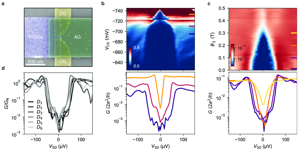
To gain insights into the quality of the Ge/PtSiGe junction we characterise transport through the superconductor-normal quantum point contact (SN-QPC) device shown in Fig. 3a. Importantly, the methodology based on spectroscopy of SN devices alleviates the ambiguity of measuring the amount of quasiparticle states inside the gap with SNS junctions Ridderbos et al. (2020). On the left side of the QPC there is a PtSiGe superconducting lead and on the right side a normal lead consisting of a 2DHG accumulated in the Ge QW. With the accumulation gate (AG) set at large negative voltages to populate the QW we apply a more positive voltage to the constriction gates (CG), creating a tunable barrier between the superconducting and the normal region. In Fig. 3b we progressively decrease the barrier height (decreasing ) going from the tunneling regime, where conductance is strongly suppressed, to a more open regime where conductance approaches the single conductance quantum . Line-cuts of the conductance color map are presented in the bottom panel of Fig. 3c. In the tunneling regime, we observe a hard induced superconducting gap, characterised by a two orders of magnitude suppression of the in-gap conductance to the normal-state conductance, and the arising of coherence peaks at . Fig. 3b also shows that the induced superconducting gap varies with the constriction gate voltage. A possible explanation is that, upon increasing the density in the semiconductor nearby the junction, the coupling to the parent superconductor might vary, as also observed in other hybrid nanostructures De Moor et al. (2018).
The evolution of the gap as a function of in-plane magnetic field () shown in Fig. 3c confirms that the gap remains hard for finite magnetic fields up to , ultimately vanishing at T. The magnetic field evolution of the gap in all three directions matches the behaviour observed in the SNS-QPC (Supplementary Fig. S7).
Finally, Fig. 3d reports the conductance traces in tunneling regime for all the six measured devices (an overview of the geometries of these devices and the respective measurements are available in the Supplementary Fig. S8, the conductance maps for all these devices are shown in Supplementary Fig. S9). For all devices we observe suppression of conductance equal or larger than two orders of magnitude. At a quantitative level, the conductance traces of Fig 3d are well fitted by the BTK theory Blonder et al. (1982) (Supplementary Fig. S9) consistent with a hard induced superconducting gap free of subgap states Heedt et al. (2021); Chang et al. (2015). This finding is the signature of a robust process that yields a reproducible high-quality superconductor-semiconductor interface, overcoming a long-standing challenge for hybrid superconductor-semiconductor quantum devices in Ge.
.4 Superconducting quantum interference devices
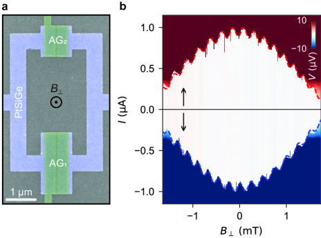
We use the superconducting quantum interference device (SQUID) in Fig. 4a to demonstrate phase control across a Josephson junction, an important ingredient for achieving topological states at low magnetic field Pientka et al. (2017a); Fornieri et al. (2019b); Ren et al. (2019); Luethi et al. (2022). The device is composed of two Josephson field-effect transistors (JoFETs) with a width of and for JoFET and JoFET respectively, and equal length of . The critical current of the junctions and can be tuned independently by applying the accumulation gate voltages and to the corresponding gates. We investigate the oscillations of the SQUID switching current as a function of the out-of-plane-magnetic field penetrating the SQUID loop. Namely, we set and , such that both arms support supercurrent and . This condition provides that the first junction is used as a reference junction and that the phase drop on it is flux independent, while the phase drop over the second junction is therefore modulated by the external flux through the loop. This allows the measurement of the current-phase-relation (CPR) of the second junction. This is demonstrated in Fig. 4b where the shown SQUID oscillations are well fitted by the relation: where are the Fraunhofer dependencies of the critical current obtained from fitting the Fraunhofer pattern of each junction (Supplementary Fig. S10), are the junction areas, is the out-of-plane magnetic field and the flux quantum. From the fit of the data in Fig. 4b (red dashed-line) we extract the effective SQUID loop area (comparable to the SQUID geometric area) and the self-inductance . In order to confirm for the self-inductance effects, we also fit SQUID oscillations for the opposite direction of the current bias (blue dashed-line) and we get similar values for the effective loop area and self-inductance.
.5 Scalable junctions
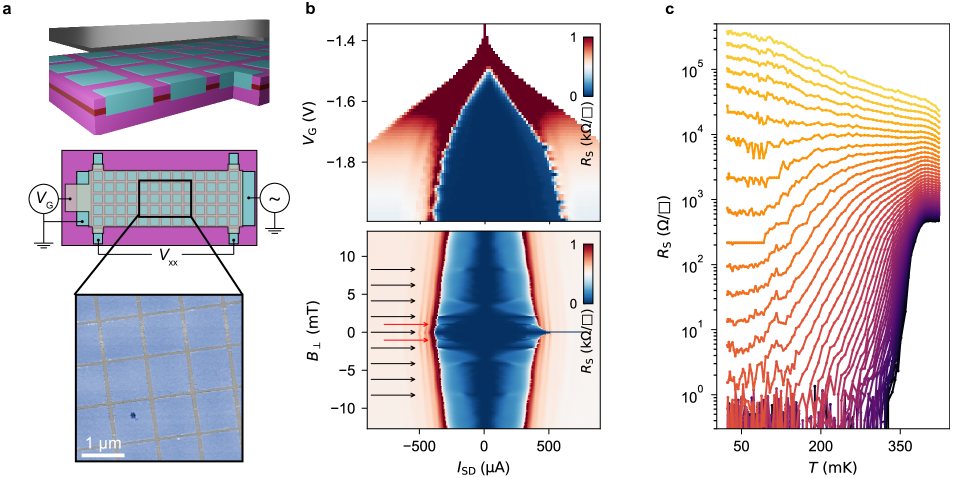
As a first step towards monolithic superconductor-semiconductor quantum circuits in two dimensions, we fabricate and study transport in a macroscopic hybrid device comprising a large array of 510 PtSiGe islands (Fig. 5a) and a global top gate. Each pair of neighbouring islands forms a Josephson junction whose transparency can be tuned by the global accumulation gate. The top panel of Fig. 5b shows a current bias measurement of the junctions array resistance. As the accumulation gate becomes more negative, all the junctions are proximitized and a supercurrent flows through the device. Remarkably, as the source-drain current approaches the junctions critical current the whole array simultaneously switches from superconducting to resistive regime, as shown from the sharp resistance step (Fig. 5b top).
With this device we also study the evolution of the switching current in a small perpendicular magnetic field. In the bottom panel of Fig. 5b we observe Fraunhofer-like interference, along with the fingerprint of flux commensurability effects associated with the periodicity of the array. At integer numbers of flux quantum per unit area of the periodic array , where with the junction area and the flux quanta, we observe switching current peaks at , , , and , denoted by a black arrow in the plot. We also notice this effect at fractional values of , most notably at (red arrow). Flux commensurability effects, due to the pinning and interference of vortices in Josephson junctions arrays, have been previously reported Poccia et al. (2015); Bøttcher et al. (2018).
The observation of simultaneous switching of super-current and of the Fraunhofer pattern with flux commensurability effects, suggests that all islands effective areas are similar and that the supercurrent through the various junctions is comparable, meaning that all junctions respond synchronously to the applied gate voltage. This is further supported by the observation of sharp switching of super-current and the Fraunhofer pattern of a 1D array of superconducting islands presented in Supplementary Fig. S11.
Finally we present in Fig. 5b the sheet resistance as a function of temperature for different gate voltages. As the gate voltage becomes more negative, the coupling between neighbouring superconducting islands increases and the system transitions from an insulating to a superconducting regime. At low gate voltage the resistance increases with decreasing temperature (yellow curves) indicating the insulating state, while at high gates the resistance drops to zero (purple curves) owing to the global superconducting state. At intermediate gate voltages (, orange curves) there is a transition where the resistance shows a weak temperature dependence. It will be interesting to study this regime in detail, in light of the recent claims of an anomalous metallic state between the superconducting and the insulating phases Bøttcher et al. (2018).
.6 Conclusions
In conclusion, we have developed superconducting germanosilicides for contacting Ge quantum wells, which has resulted in excellent superconducting properties imparted to the high-mobility 2DHG. We induced a hard superconducting gap in Ge, a large advancement compared to previous work on Ge hybrid superconductor-semiconductor devices Hendrickx et al. (2019); Vigneau et al. (2019); Aggarwal et al. (2021); Ridderbos et al. (2019). We were able to observe a hard gap with 100% yield across all the six measured devices, pointing to a robust and reproducible fabrication process. Next to this central result, we further demonstrate phase control across a Josephson junction and take advantage of the planar geometry to scale these devices in 2D arrays.
While we focused on the poly-crystalline superconducting PtSiGe compound, we anticipate two strategies to further increase the size of the induced superconducting gap, which sets a relevant energy scale for hybrid devices. Firstly, following the approach in ref. Aggarwal et al. (2021) a superconducting layer with a larger gap, such as Al or Nb, may be deposited on top of the superconducting PtSiGe. Secondly, other ternary superconducting germanosilicides with a higher critical temperature may be explored, starting from the deposition and thermal anneal of other platinoid metals such as Rh and Ir Matthias et al. (1963).
Based on our findings, we foresee the following use cases for superconductor-semiconductor hybrids in high mobility planar Ge. With the challenge of a hard gap addressed, planar Ge appears a promising platform to host Majorana bound states in phased-biased Josephson junctions Hell et al. (2017); Pientka et al. (2017b); Fornieri et al. (2019a). Calculations with experimentally realistic material parameters Luethi et al. (2022) show that accessing the topological phase is feasible by careful design of Ge planar Josephson junctions geometries that relaxes magnetic field and spin-orbit constrains.
Crucially, the realization of a hard superconducting gap positions planar Ge as a unique material platform to pursue the coherent coupling of high fidelity spin qubits using crossed Andreev reflection to enable two-qubit gates over micrometer distances Choi et al. (2000); Leijnse and Flensberg (2013). Remote coupling of spin qubits in Ge may also be achieved by coupling spin qubits via superconducting quantum dots Choi et al. (2000); Leijnse and Flensberg (2011), potentially offering a topological protectionKitaev (2001). Coupling on an even longer distance may be obtained via superconducting resonators Burkard et al. (2020). In such a scenario, a capacitive interaction may suffice, but connecting the resonator to a superconducting ohmic, such as PtSiGe, could result in a larger lever arm and therefore boost the coupling, while a direct tunnel coupling would give further directions to explore. The ability to couple qubits over different length scales is highly relevant and a critical component in network-based quantum computing Vandersypen et al. (2017).
Furthermore, the demonstration of a hard gap in Ge motivates the investigation of alternative spin qubits systems, such as Andreev spin qubits (ASQ) Chtchelkatchev and Nazarov (2003); Padurariu and Nazarov (2010), that may be coupled with gatemons Pita-Vidal et al. (2022) or superconductors Spethmann et al. (2022). Similar to semiconductor spin qubits, the use of isotopically purified Ge Itoh and Watanabe (2014) may overcome the strong decoherence from the nuclear environment currently limiting progress with ASQs in III-V materials Hays et al. (2021); Pita-Vidal et al. (2022).
All together, these findings represent a major step in the Ge quantum information route, aiming to co-integrate spin, superconducting, and topological systems for scalable and high-fidelity quantum information processing on a silicon wafer.
References
- Lutchyn et al. (2018) R. M. Lutchyn, E. P. Bakkers, L. P. Kouwenhoven, P. Krogstrup, C. M. Marcus, and Y. Oreg, Nature Reviews Materials 3, 52 (2018).
- Flensberg et al. (2021) K. Flensberg, F. von Oppen, and A. Stern, Nature Reviews Materials 6, 944 (2021).
- Hays et al. (2021) M. Hays, V. Fatemi, D. Bouman, J. Cerrillo, S. Diamond, K. Serniak, T. Connolly, P. Krogstrup, J. Nygård, A. Levy Yeyati, A. Geresdi, and M. H. Devoret, Science 373, 430 (2021).
- Casparis et al. (2018) L. Casparis, M. R. Connolly, M. Kjaergaard, N. J. Pearson, A. Kringhøj, T. W. Larsen, F. Kuemmeth, T. Wang, C. Thomas, S. Gronin, G. C. Gardner, M. J. Manfra, C. M. Marcus, and K. D. Petersson, Nature Nanotechnology 13, 915 (2018).
- Choi et al. (2000) M.-S. Choi, C. Bruder, and D. Loss, Physical Review B 62, 13569 (2000).
- Leijnse and Flensberg (2011) M. Leijnse and K. Flensberg, Physical Review Letters 107, 210502 (2011).
- Leijnse and Flensberg (2012) M. Leijnse and K. Flensberg, Physical Review B - Condensed Matter and Materials Physics 86, 104511 (2012).
- Hoffman et al. (2016) S. Hoffman, C. Schrade, J. Klinovaja, and D. Loss, Physical Review B 94, 045316 (2016).
- Leijnse and Flensberg (2013) M. Leijnse and K. Flensberg, Physical Review Letters 111, 060501 (2013).
- Kitaev (2001) A. Y. Kitaev, Physics-Uspekhi 44, 131 (2001).
- Chang et al. (2015) W. Chang, S. M. Albrecht, T. S. Jespersen, F. Kuemmeth, P. Krogstrup, J. Nygård, and C. M. Marcus, Nature Nanotechnology 10, 232 (2015).
- Kjaergaard et al. (2016) M. Kjaergaard, F. Nichele, H. J. Suominen, M. P. Nowak, M. Wimmer, A. R. Akhmerov, J. A. Folk, K. Flensberg, J. Shabani, C. J. Palmstrøm, and C. M. Marcus, Nature Communications 7, 1 (2016).
- Fornieri et al. (2019a) A. Fornieri, A. M. Whiticar, F. Setiawan, E. Portolés, A. C. C. Drachmann, A. Keselman, S. Gronin, C. Thomas, T. Wang, R. Kallaher, G. C. Gardner, E. Berg, M. J. Manfra, A. Stern, C. M. Marcus, and F. Nichele, Nature 569, 89 (2019a).
- Aghaee et al. (2022) M. Aghaee, A. Akkala, Z. Alam, R. Ali, A. A. Ramirez, M. Andrzejczuk, A. E. Antipov, P. Aseev, M. Astafev, B. Bauer, J. Becker, S. Boddapati, F. Boekhout, J. Bommer, E. B. Hansen, T. Bosma, L. Bourdet, S. Boutin, P. Caroff, L. Casparis, M. Cassidy, A. W. Christensen, N. Clay, W. S. Cole, F. Corsetti, A. Cui, P. Dalampiras, A. Dokania, G. de Lange, M. de Moor, J. C. E. Saldaña, S. Fallahi, Z. H. Fathabad, J. Gamble, G. Gardner, D. Govender, F. Griggio, R. Grigoryan, S. Gronin, J. Gukelberger, S. Heedt, J. H. Zamorano, S. Ho, U. L. Holgaard, W. H. P. Nielsen, H. Ingerslev, P. J. Krogstrup, L. Johansson, J. Jones, R. Kallaher, F. Karimi, T. Karzig, C. King, M. E. Kloster, C. Knapp, D. Kocon, J. Koski, P. Kostamo, M. Kumar, T. Laeven, T. Larsen, K. Li, T. Lindemann, J. Love, R. Lutchyn, M. Manfra, E. Memisevic, C. Nayak, B. Nijholt, M. H. Madsen, S. Markussen, E. Martinez, R. McNeil, A. Mullally, J. Nielsen, A. Nurmohamed, E. O’Farrell, K. Otani, S. Pauka, K. Petersson, L. Petit, D. Pikulin, F. Preiss, M. Q. Perez, K. Rasmussen, M. Rajpalke, D. Razmadze, O. Reentila, D. Reilly, R. Rouse, I. Sadovskyy, L. Sainiemi, S. Schreppler, V. Sidorkin, A. Singh, S. Singh, S. Sinha, P. Sohr, T. Stankevič, L. Stek, H. Suominen, J. Suter, V. Svidenko, S. Teicher, M. Temuerhan, N. Thiyagarajah, R. Tholapi, M. Thomas, E. Toomey, S. Upadhyay, I. Urban, S. Vaitiekėnas, K. Van Hoogdalem, D. V. Viazmitinov, S. Waddy, D. Van Woerkom, D. Vogel, J. Watson, J. Weston, G. W. Winkler, C. K. Yang, S. Yau, D. Yi, E. Yucelen, A. Webster, R. Zeisel, and R. Zhao, “InAs-Al Hybrid Devices Passing the Topological Gap Protocol,” (2022), arXiv:2207.02472 [cond-mat].
- Dvir et al. (2022) T. Dvir, G. Wang, N. van Loo, C.-X. Liu, G. P. Mazur, A. Bordin, S. L. D. t. Haaf, J.-Y. Wang, D. van Driel, F. Zatelli, X. Li, F. K. Malinowski, S. Gazibegovic, G. Badawy, E. P. A. M. Bakkers, M. Wimmer, and L. P. Kouwenhoven, “Realization of a minimal Kitaev chain in coupled quantum dots,” (2022), arXiv:2206.08045 [cond-mat].
- Cywiński et al. (2009) L. Cywiński, W. M. Witzel, and S. Das Sarma, Physical Review Letters 102, 1 (2009).
- Stano and Loss (2022) P. Stano and D. Loss, Nature Reviews Physics 4, 672 (2022).
- Scappucci et al. (2020) G. Scappucci, C. Kloeffel, F. A. Zwanenburg, D. Loss, M. Myronov, J. J. Zhang, S. De Franceschi, G. Katsaros, and M. Veldhorst, Nature Reviews Materials 6, 926–943 (2020).
- Watzinger et al. (2018) H. Watzinger, J. Kukučka, L. Vukušić, F. Gao, T. Wang, F. Schäffler, J. J. Zhang, and G. Katsaros, Nature Communications 9, 1 (2018).
- Hendrickx et al. (2020) N. W. Hendrickx, D. P. Franke, A. Sammak, G. Scappucci, and M. Veldhorst, Nature 577, 487 (2020).
- Jirovec et al. (2021) D. Jirovec, A. Hofmann, A. Ballabio, P. M. Mutter, G. Tavani, M. Botifoll, A. Crippa, J. Kukucka, O. Sagi, F. Martins, J. Saez-Mollejo, I. Prieto, M. Borovkov, J. Arbiol, D. Chrastina, G. Isella, and G. Katsaros, Nature Materials 20, 1106 (2021).
- Prechtel et al. (2016) J. H. Prechtel, A. V. Kuhlmann, J. Houel, A. Ludwig, S. R. Valentin, A. D. Wieck, and R. J. Warburton, Nature Materials 15, 981 (2016).
- Itoh and Watanabe (2014) K. M. Itoh and H. Watanabe, MRS Communications 4, 143 (2014).
- Lodari et al. (2019) M. Lodari, A. Tosato, D. Sabbagh, M. A. Schubert, G. Capellini, A. Sammak, M. Veldhorst, and G. Scappucci, Physical Review B 100 (2019), 10.1103/PhysRevB.100.041304.
- Lodari et al. (2022) M. Lodari, O. Kong, M. Rendell, A. Tosato, A. Sammak, M. Veldhorst, A. R. Hamilton, and G. Scappucci, Applied Physics Letters 120, 122104 (2022).
- Hendrickx et al. (2021) N. W. Hendrickx, W. I. Lawrie, M. Russ, F. van Riggelen, S. L. de Snoo, R. N. Schouten, A. Sammak, G. Scappucci, and M. Veldhorst, Nature 591, 580 (2021).
- Borsoi et al. (2022) F. Borsoi, N. W. Hendrickx, V. John, S. Motz, F. van Riggelen, A. Sammak, S. L. de Snoo, G. Scappucci, and M. Veldhorst, “Shared control of a 16 semiconductor quantum dot crossbar array,” (2022), arXiv:2209.06609 [cond-mat, physics:quant-ph].
- Dimoulas et al. (2006) A. Dimoulas, P. Tsipas, A. Sotiropoulos, and E. K. Evangelou, Applied Physics Letters 89, 252110 (2006).
- Hendrickx et al. (2018) N. W. Hendrickx, D. P. Franke, A. Sammak, M. Kouwenhoven, D. Sabbagh, L. Yeoh, R. Li, M. L. Tagliaferri, M. Virgilio, G. Capellini, G. Scappucci, and M. Veldhorst, Nature Communications 9, 2835 (2018).
- Hendrickx et al. (2019) N. W. Hendrickx, M. L. Tagliaferri, M. Kouwenhoven, R. Li, D. P. Franke, A. Sammak, A. Brinkman, G. Scappucci, and M. Veldhorst, Physical Review B 99, 7 (2019).
- Ridderbos et al. (2019) J. Ridderbos, M. Brauns, J. Shen, F. K. de Vries, A. Li, S. Kölling, M. A. Verheijen, A. Brinkman, W. G. van der Wiel, E. P. A. M. Bakkers, and F. A. Zwanenburg, (2019).
- Vigneau et al. (2019) F. Vigneau, R. Mizokuchi, D. C. Zanuz, X. Huang, S. Tan, R. Maurand, S. Frolov, A. Sammak, G. Scappucci, F. Lefloch, and S. De Franceschi, Nano Letters 19, 1023 (2019).
- Aggarwal et al. (2021) K. Aggarwal, A. Hofmann, D. Jirovec, I. Prieto, A. Sammak, M. Botifoll, S. Martí-Sánchez, M. Veldhorst, J. Arbiol, G. Scappucci, J. Danon, and G. Katsaros, Physical Review Research 3, L022005 (2021).
- Kittl et al. (2008) J. A. Kittl, K. Opsomer, C. Torregiani, C. Demeurisse, S. Mertens, D. P. Brunco, M. J. Van Dal, and A. Lauwers, Materials Science and Engineering B 154, 144 (2008).
- Sammak et al. (2019) A. Sammak, D. Sabbagh, N. W. Hendrickx, M. Lodari, B. Paquelet Wuetz, A. Tosato, L. Yeoh, M. Bollani, M. Virgilio, M. A. Schubert, P. Zaumseil, G. Capellini, M. Veldhorst, and G. Scappucci, Advanced Functional Materials 29, 1807613 (2019).
- Ahn et al. (2021) S. Ahn, H. Pan, B. Woods, T. D. Stanescu, and S. D. Sarma, Physical Review Materials 5, 124602 (2021).
- Vandersypen et al. (2017) L. M. K. Vandersypen, H. Bluhm, J. S. Clarke, A. S. Dzurak, R. Ishihara, A. Morello, D. J. Reilly, L. R. Schreiber, and M. Veldhorst, npj Quantum Information , 1 (2017).
- Gaudet et al. (2006) S. Gaudet, C. Detavernier, A. J. Kellock, P. Desjardins, and C. Lavoie, Journal of Vacuum Science & Technology A: Vacuum, Surfaces, and Films 24, 474 (2006).
- Shabani et al. (2016) J. Shabani, M. Kjaergaard, H. J. Suominen, Y. Kim, F. Nichele, K. Pakrouski, T. Stankevic, R. M. Lutchyn, P. Krogstrup, R. Feidenhans’L, S. Kraemer, C. Nayak, M. Troyer, C. M. Marcus, and C. J. Palmstrøm, Physical Review B 93, 1 (2016).
- Alptekin et al. (2009) E. Alptekin, C. J. Kirkpatrick, V. Misra, and M. C. Ozturk, IEEE Transactions on Electron Devices 56, 1220 (2009).
- Irie et al. (2014) H. Irie, Y. Harada, H. Sugiyama, and T. Akazaki, Physical Review B - Condensed Matter and Materials Physics 89, 1 (2014).
- Ambegaokar and Baratoff (1963) V. Ambegaokar and A. Baratoff, Physical Review Letters 10, 486 (1963).
- Heedt et al. (2021) S. Heedt, M. Quintero-Pérez, F. Borsoi, A. Fursina, N. van Loo, G. P. Mazur, M. P. Nowak, M. Ammerlaan, K. Li, S. Korneychuk, J. Shen, M. A. Y. van de Poll, G. Badawy, S. Gazibegovic, N. de Jong, P. Aseev, K. van Hoogdalem, E. P. Bakkers, and L. P. Kouwenhoven, Nature Communications 12, 1 (2021).
- Tinkham (1996) M. Tinkham, Introduction to superconductivity (McGraw-Hill, 1996).
- Octavio et al. (1983) M. Octavio, M. Tinkham, G. E. Blonder, and T. M. Klapwijk, Physical Review B 27, 6739 (1983).
- Kjaergaard et al. (2017) M. Kjaergaard, H. J. Suominen, M. P. Nowak, A. R. Akhmerov, J. Shabani, C. J. Palmstrøm, F. Nichele, and C. M. Marcus, Physical Review Applied 7, 034029 (2017).
- Averin and Bardas (1995) D. Averin and A. Bardas, Physical Review Letters 75, 1831 (1995).
- Borsoi et al. (2021) F. Borsoi, G. P. Mazur, N. van Loo, M. P. Nowak, L. Bourdet, K. Li, S. Korneychuk, A. Fursina, J. Wang, V. Levajac, E. Memisevic, G. Badawy, S. Gazibegovic, K. van Hoogdalem, E. P. A. M. Bakkers, L. P. Kouwenhoven, S. Heedt, and M. Quintero‐Pérez, Advanced Functional Materials 31, 2102388 (2021).
- Fornieri et al. (2019b) A. Fornieri, A. M. Whiticar, F. Setiawan, E. Portolés, A. C. Drachmann, A. Keselman, S. Gronin, C. Thomas, T. Wang, R. Kallaher, G. C. Gardner, E. Berg, M. J. Manfra, A. Stern, C. M. Marcus, and F. Nichele, Nature 569, 89 (2019b).
- Nilsson et al. (2012) H. A. Nilsson, P. Samuelsson, P. Caroff, and H. Q. Xu, Nano Lett 12, 233 (2012).
- Ridderbos et al. (2020) J. Ridderbos, M. Brauns, F. de Vries, J. Shen, A. Li, S. Kölling, M. Verheijen, A. Brinkman, W. van der Wiel, E. Bakkers, E. Bakkers, and F. Zwanenburg, Nano letters 20, 122 (2020).
- De Moor et al. (2018) M. W. De Moor, J. D. Bommer, D. Xu, G. W. Winkler, A. E. Antipov, A. Bargerbos, G. Wang, N. V. Loo, R. L. Op Het Veld, S. Gazibegovic, D. Car, J. A. Logan, M. Pendharkar, J. S. Lee, E. P. M Bakkers, C. J. Palmstrom, R. M. Lutchyn, L. P. Kouwenhoven, and H. Zhang, New Journal of Physics 20, 103049 (2018).
- Blonder et al. (1982) G. E. Blonder, M. Tinkham, and T. M. Klapwijk, Physical Review B 25, 4515 (1982).
- Pientka et al. (2017a) F. Pientka, A. Keselman, E. Berg, A. Yacoby, A. Stern, and B. I. Halperin, Physical Review X 7, 1 (2017a).
- Ren et al. (2019) H. Ren, F. Pientka, S. Hart, A. T. Pierce, M. Kosowsky, L. Lunczer, R. Schlereth, B. Scharf, E. M. Hankiewicz, L. W. Molenkamp, B. I. Halperin, and A. Yacoby, Nature 569, 93 (2019).
- Luethi et al. (2022) M. Luethi, K. Laubscher, S. Bosco, D. Loss, and J. Klinovaja, “Planar Josephson junctions in germanium: Effect of cubic spin-orbit interaction,” (2022), arXiv:2209.12745 [cond-mat].
- Poccia et al. (2015) N. Poccia, T. I. Baturina, F. Coneri, C. G. Molenaar, X. R. Wang, G. Bianconi, A. Brinkman, H. Hilgenkamp, A. A. Golubov, and V. M. Vinokur, Science 349, 1202 (2015).
- Bøttcher et al. (2018) C. G. Bøttcher, F. Nichele, M. Kjaergaard, H. J. Suominen, J. Shabani, C. J. Palmstrøm, and C. M. Marcus, Nature Physics 14, 1138 (2018).
- Matthias et al. (1963) B. T. Matthias, T. H. Geballe, and V. B. Compton, Reviews of Modern Physics 35, 1 (1963).
- Hell et al. (2017) M. Hell, M. Leijnse, and K. Flensberg, Physical Review Letters 118, 107701 (2017).
- Pientka et al. (2017b) F. Pientka, A. Keselman, E. Berg, A. Yacoby, A. Stern, and B. I. Halperin, Physical Review X 7, 021032 (2017b).
- Burkard et al. (2020) G. Burkard, M. J. Gullans, X. Mi, and J. R. Petta, Nature Reviews Physics 2, 129 (2020).
- Chtchelkatchev and Nazarov (2003) N. M. Chtchelkatchev and Y. V. Nazarov, Physical Review Letters 90, 226806 (2003).
- Padurariu and Nazarov (2010) C. Padurariu and Y. V. Nazarov, Physical Review B 81, 144519 (2010).
- Pita-Vidal et al. (2022) M. Pita-Vidal, A. Bargerbos, R. Žitko, L. J. Splitthoff, L. Grünhaupt, J. J. Wesdorp, Y. Liu, L. P. Kouwenhoven, R. Aguado, B. van Heck, A. Kou, and C. K. Andersen, “Direct manipulation of a superconducting spin qubit strongly coupled to a transmon qubit,” (2022), arXiv:2208.10094 [cond-mat, physics:quant-ph].
- Spethmann et al. (2022) M. Spethmann, X.-P. Zhang, J. Klinovaja, and D. Loss, Physical Review B 106, 115411 (2022), arXiv:2205.03843 [cond-mat, physics:quant-ph].
- Nowak et al. (2019) M. P. Nowak, M. Wimmer, and A. R. Akhmerov, Physical Review B 99, 075416 (2019).
I Methods
Ge/SiGe heterostructure growth. The Ge/SiGe heterostructure of this study is grown on a 100-mm n-type Si(001) substrate using an Epsilon 2000 (ASMI) reduced pressure chemical vapor deposition reactor. The layer sequence comprises a virtual substrate obtained by reverse grading, a thick Ge quantum well, a -thick barrier, and a thin sacrificial Si cap Sammak et al. (2019). Detailed electrical characterisation of heterostructure field effect transistors from these heterostructures are presented in ref. Sammak et al. (2019).
Device fabrication. The fabrication of the devices presented in this paper entails the following steps. Wet etching of the sacrificial Si-cap in buffer oxide etch for . Deposition of the Pt contacts via e-gun evaporation of of Pt at pressure of at the rate of . Rapid thermal anneal of Pt contacts at