Dynamic negative capacitance regime in GeTe Rashba ferroelectric.
Abstract
We experimentally investigate capacitance response of a thick ferroelectric GeTe single-crystal flake on the Si/SiO2 substrate, where p-doped Si layer serves as a gate electrode. We confirm by resistance measurements, that for three-dimensional flakes, electron concentration is not sensitive to the gate electric field due to the screening by bulk carriers. Unexpectedly, we observe that sample capacitance is strongly diminishing for both gate field polarities, so is a maximum near the zero gate voltage. Also, we observe well-developed hysteresis with the gate voltage sweep direction for the experimental curves. From our analysis, the capacitance behavior is explained by the known dependence of the Rashba parameter on the electric field for giant Rashba splitting in GeTe. In this case, the hysteresis in capacitance should be ascribed to polarization evolution in GeTe surface layers, which also allows to realize the regime of dynamic negative capacitance. The latter can be directly observed in time-dependent resistive measurements, as non-monotonic evolution of voltage response to the step-like current pulse. Thus, the negative capacitance regime can indeed improve performance and, therefore, the energy efficiency of electronic devices.
pacs:
71.30.+h, 72.15.Rn, 73.43.NqI Introduction
Recent interest to systems with broken inversion or time-reversal symmetries is mostly connected with topological materials. In Weyl semimetals (WSM), symmetry requires splitting of every Dirac point with three-dimensional linear spectrum into two Weyl nodes with different chiralities armitage . Fermi arcs are connecting projections of Weyl nodes on the surface Brillouin zone, which defines topologically protected surface state transport in topological semimetals. On the other hand, the bulk properties are also affected by symmetry. In particular, Weyl semimetals with broken time-reversal symmetry are bulk ferromagnetics or antiferromagnetics, while non-magnetic WSMs with broken inversion symmetry have to obtain ferroelectric polarization armitage ; TSreview . In addition to the gapless bulk spectrum armitage , ferroelectric polarization makes non-magnetic Weyl semimetals being the natural representation of the novel concept of the intrinsic polar metal, or the ferroelectric conductor PM ; pm1 ; pm2 ; pm3 ; pm4 .
For ordinary ferroelectric insulators, the effect of negative capacitance NC1 is attracting significant interest nowadays NC3 ; NC2 . Apart from the fundamental importance, it is expected that the negative capacitance field-effect transistor (NCFET) can further improve the energy efficiency of electronic devices NC2 ; NC4 . For a standard field-effect transistor, the capacitance between the gate and the quantum well can be written shash ; khrap as
| (1) |
where is the geometrical capacitance value, while the term is the contribution from the finite thermodynamic density of states in the quantum well (the so called quantum capacitance), is the sample area. Since is defined by the energy spectrum, capacitance spectroscopy is a powerful spectroscopic tool Dolgop , also for newest systems like graphene graph1 ; graph2 ; graph3 ; graph4 or topological insulators TI1 ; TI2 .
It is accepted to speak about negative capacitance if the measured capacitance exceeds the geometrically defined value in Eq.(1), which was firstly demonstrated for two-dimensional electron systems Eisenst ; dorozh in GaAs quantum wells. Nominally, negative capacitance requires negative thermodynamic density of states in Eq.(1), which is generally not allowed for macroscopically stable systems NC1 . For the experimentally available systems, this regime is stabilized by static external electric field, e.g. from ionized donors in quantum wells Eisenst ; dorozh ; efros or from another ferroelectric layer in NCFET NC2 ; NC_SC . Also, dynamic (transient) negative capacitance is proposed due to the polarization switching in ferroelectrics NC2 ; NC_SC . Transient negative capacitance appears for any microscopic switching mechanism as long as polarization changes faster than charge. However, the device will always end up in a state of positive capacitance after the ferroelectric has switched NC2 ; NC_SC .
Similar experiments can also be proposed for polar metals PM ; pm1 ; pm2 ; pm3 ; pm4 , or conductive ferroelectrics. In this case, screening of the gate electric field by bulk carriers allows to study only surface layer capacitance in a quasi-two-dimensional regime Eisenst ; dorozh . Among these materials, GeTe is of special interest GeTespin-to-charge ; GeTereview due to the reported giant Rashba splitting GeTerashba , which can be important also in spintronic applications. The ferroelectric control of spin-to-charge conversion was shown in epitaxial GeTe films GeTespin-to-charge , also, direct correlation between ferroelectricity and spin texture was demonstrated in this material spin text . Ferroelectric polarization is observed for the epitaxial films, microwires and bulk GeTe crystals GeTespin-to-charge , it is defined by the non-centrosymmetric distorted rhombohedral structure () with space group R3m (No. 160) GeTerashba .
Here, we experimentally investigate capacitance response of a thick ferroelectric GeTe single-crystal flake on the Si/SiO2 substrate, where p-doped Si layer serves as a gate electrode. We confirm by resistance measurements, that for three-dimensional flakes, electron concentration is not sensitive to the gate electric field due to the screening by bulk carriers. Unexpectedly, we observe well-developed hysteresis with the gate voltage sweep direction for the experimental non-linear curves. From our analysis, the hysteresis in capacitance should be ascribed to polarization evolution in GeTe surface layers, which also allows to realize the regime of dynamic negative capacitance.
II Samples and techniques
The GeTe single crystals were grown by physical vapor transport in the evacuated silica ampule. The initial GeTe load was synthesized by direct reaction of the high-purity (99.9999%) elements in vacuum. For the GeTe crystals growth, the initial load serves as the source of vapors: it was melted and kept at 770-780∘ C for 24 h. Afterward, the source was cooled down to 350∘ C at the 7.5 deg/h rate. The GeTe crystals grew during this process on the cold ampule walls somewhat above the source. The GeTe composition is verified by energy-dispersive X-ray spectroscopy. The powder X-ray diffraction analysis confirms single-phase GeTe, the known structure model GeTerashba is also refined with single crystal X-ray diffraction measurements.
For the capacitance measurements we use thick (about 0.5 m) GeTe single crystal flakes on the standard Si/SiO2 substrate. The p-doped Si layer serves as the gate electrode to apply the gate electric field through the 200 nm thick SiO2 layer, while conductive GeTe bulk allows nearly perfect field screening.
The 100 m wide flakes are obtained by mechanical exfoliation from the initial ingot. We choose the 100 m wide flakes with defect-free surface by optical microscope. A single flake is placed by the most defect-free surface on Si/SiO2 substrate with pre-defined 10 m wide Au contact leads. The leads pattern is prepared by lift-off technique after thermal evaporation of 100 nm Au. After initial single-shot pressing by another oxidized silicon substrate, no pressure is needed to hold the flake on the SiO2 surface with Au leads.
This procedure with pre-defined contacts is specially designed for thick conductive flakes, where the desired experimental geometry can not be defined by usual mesa etching. It was demonstrated to provide electrically and mechanically stable contacts with highly transparent metal-semiconductor interfaces and it also allows to avoid chemical or thermal treatment of the initial materials black ; SnSeour1 ; SnSeour2 ; WTeour ; WTe2shapiro ; WTe2chiral . Also, the relevant (bottom) GeTe surface is protected from any oxidation or contamination by a SiO2 substrate and thick GeTe bulk. This is an important difference from conventional monolayers, so we never observed surface degradation for the present sample design black ; SnSeour1 ; SnSeour2 ; WTeour ; WTe2shapiro ; WTe2chiral .
Even for relatively thick flakes, ferroelectric polarization is sensitive WTeour to the gate electric field, since the relevant (bottom) flake surface is directly adjoined to the SiO2 layer.
To obtain dependences of the sample capacitance on the dc gate voltage , gate bias is applied between the silicon substrate and one of the Au leads, see the inset to Fig. 1. The dc bias is modulated by a low ac component. Both the imaginary and real ac current components are measured in the circuit by lock-in.
Au leads also allow resistance measurements for GeTe flakes. We obtain or curves in a two-point technique for the direct comparison with the two-point capacitance measurements: contact resistances always have some effect in capacitance measurements as non-zero real ac current component. For the resistive measurements, the applied current is also modulated by low (0.1 mA) ac component, two-point ac voltage () is obtained as a function of the dc source-drain current ( mA) or the dc gate voltage .
We check directly by the gate electrometer that there is no measurable leakage current through the 200 nm thick SiO2 layer at least in the gate voltage range V. In the present setup, SiO2 substrate protects the flake from further oxidation/contamination black , while the ferroelectric phase exists Tc below K. Thus, all the measurements are performed at room temperature under ambient conditions.
III Experimental results
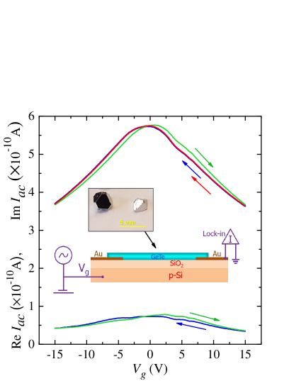
Fig. 1 shows both ac current components for two opposite gate voltage sweep directions. A typical gated sample can be described by RC circuit model, where is the gate capacitance while is the characteristic circuit resistance shash ; khrap ; dorozh . For the chosen ac modulation frequency , we obtain in Fig. 1 with strictly linear dependence within 100 to 1000 Hz frequency range. For this reason, the capacitance dominates in the sample impedance shash ; khrap ; dorozh .
There are two nontrivial experimental observations in Fig. 1 in comparison with usual curves for standard field-effect devices. First, the sample capacitance is monotonously diminishing for both gate voltage polarities with a maximum around zero , so the experimental curves are nearly symmetric.
As the second observation, Fig. 1 shows well-developed hysteresis of the experimental curves with gate voltage sweep direction. It is important, that two experimental curves are well reproducible for the same sweep direction, as it is also depicted in Fig. 1, so the sample is perfectly stable. The hysteresis can not be expected for our electrical circuit, because of the negligible charging constant RC, which is well below for the regime. The hysteresis can not be also connected with standard SiO2 dielectric, which we have verified in the independent tests. Thus, the hysteresis in capacitance should be ascribed to the slow polarization evolution SnSeour1 ; SnSeour2 ; WTeour in GeTe surface layers.
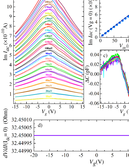
Fig. 2 (a-b) confirms the independence of the measured capacitance on the ac modulation voltage amplitude. Experimental curves are shown for two opposite sweep directions in Fig. 2 (a) for values from 10 to 200 mV. At zero gate voltage, we demonstrate strictly linear dependence in Fig. 2 (b), as it should be expected in a linear regime of Eq. (1), the slope corresponds to pF value. The latter gives effective sample area, which is a reasonable estimation for the 100 m wide GeTe flake.
For every modulation voltage , the hysteresis amplitude can be extracted as the difference between two sweeps , the result is shown in Fig. 2 (c) as the capacitance difference . All the curves are perfectly scaled into the single dependence, so is only determined by the gate voltage sweep direction. Also, does not depend on the magnitude of the sweep, so is not determined by surface degradation. As an additional argument, the latter should affect the geometrical capacitance through the effective thickness , while we demonstrate perfectly linear dependence in Fig. 2 (b).
In contrast to the standard two-dimensional materials like graphene or field-effect transistors, carrier concentration in thick conductive GeTe flakes should not be sensitive to the gate electric field due to the screening of the gate electric field by bulk carriers. Fig. 2 (d) shows constant two-point differential sample resistance in wide gate voltage range. The measured resistance Ohm allows also to estimate the RC circuit constant as s .
We wish to emphasize that, despite significant effect of the gate electric field on the capacitance (i.e. on the density of states in Eq. (1)), it has no effect on the carrier concentration itself. This behavior also indicates the ferroelectric polarization effects SnSeour1 ; SnSeour2 ; WTeour in GeTe surface layers.
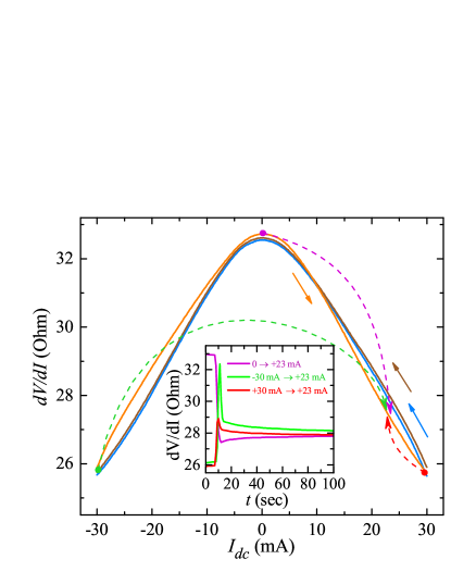
For the two-point resistance measurements, non-linear curves show hysteresis with current sweep direction in Fig. 3, which is a known fingerprint of conductive ferroelectrics WTeour ; SnSeour1 ; SnSeour2 . Current-induced source-drain field shifts the ferroelectric domain walls in the sample, which results in additional polarization current. The latter is connected with lattice deformation in ferroelectrics, and, therefore with slow resistance relaxation. The relaxation can be directly demonstrated by time-dependent curves in the inset to Fig. 3. For this curves, the sample resistance is stabilized for a long time at one of the distinct bias values +30 mA,-30 mA, or 0 mA. Afterward, the bias is abruptly changed to mA and the time-dependent relaxation is recorded for the 100 s interval. The obtained curves indeed show slow relaxation from different starting resistance values to the final one in the inset to Fig. 3. It seems to be important, that relaxation is not monotonic in the inset to Fig. 3: every curve firstly overshoots the final value, and slowly approaches to it afterward. This non-monotonic relaxation is unusual for the trivial discharging -like process, but can be expected for the dynamic (transient) negative capacitance in ferroelectrics NC2 ; NC_SC , so it can reflect the ferroelectric polarization dynamics in GeTe.
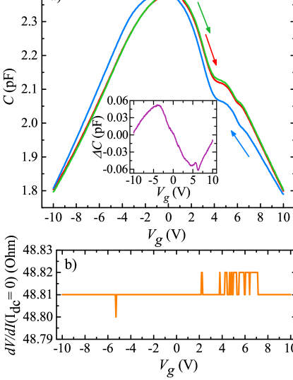
The reported behavior can be well reproduced for a different GeTe sample in Fig. 4. We demonstrate the qualitatively similar results for the symmetric dependence with hysteresis, the hysteresis amplitude, and the gate-independent differential resistance . One can also estimate constant for this GeTe structure as F s from the absolute and values.
IV Discussion
Even qualitative behavior in Figs. 1 and 4 seems to be very unusual because of symmetric diminishing of the capacitance for both gate voltage polarities.
For a two-dimensional electron gas in standard field-effect transistors, is a constant in zero magnetic field because of parabolic energy spectrum for electrons, so the capacitance is independent of the gate electric field Dolgop ; shash ; khrap in Eq. (1). For graphene samples with linear , the capacitance lozovik grows symmetrically to both sides of the charge neutrality point graph1 ; graph2 ; graph3 ; graph4 . Similar growth has been observed also for three-dimensional topological insulators TI1 ; TI2 . In these structures, the capacitance reflects the charge accumulation at the interface (the so called field effect).
In our experiment, we observe symmetric diminishing of the capacitance in Figs. 1 and 4, while there is no any effect of the gate electric field on the carrier concentration in Figs. 2 (d) and 4 (b). The latter still can be estimated in the capacitor approximation as for the sample from Fig. 4 (b). This ratio is quite low due to the high carrier concentration in three-dimensional GeTe ( cm-3) in comparison with two-dimensional systems like monolayers and quantum wells (cm-2 for the typical 10 nm thickness). In a capacitor, the concentration variation is the primary effect of the gate voltage, despite some effect on the mobility can not be also excluded.
In contrast to the mentioned above structures, GeTe is characterized by giant Rashba spin-orbit coupling GeTereview , so the Rashba term is dominant in density of states. Since the carrier concentration is independent of the gate electric field in our samples (see Figs. 2 (d) and 4 (b)), it is the Rashba parameter which defines the behavior in Figs. 1 and 4. The dependence of the Rashba parameter on the ferroelectric polarization is known for giant Rashba splitting in GeTe from theoretical GeTerashba and experimental spin text investigations. Even full reversal of the Rashba parameter can be achieved upon reversal of the electric field GeTerashba .
The total device capacitance should be written as
| (2) |
The first term is a constant (geometrical capacitance), while the second (quantum capacitance) should be responsible for the gate voltage dependence. The total value is diminishing, if the second term () is increasing in Eq,(2) increase with gate voltage. Since we are sure, that carrier concentration is independent on (see above), we can write the quantum capacitance for the dominant Rashba term as
which gives required for the known gate-field dependent giant Rashba splitting in GeTe GeTerashba . For the significant effect, the maximum value of this quantum capacitance should be of the same order as the geometrical one. The latter is estimated above from the experimental data as nF, as well as the effective sample area . The sheet density can be estimated as cm-2 from the GeTe bulk value (cm-3) for the 10 nm effective layer thickness. For these parameters, the criterion is achieved for the known eVÅ for GeTe GeTerashba . This estimation confirms our conclusion on the diminishing in Figs. 1 and 4.
Noteworthy, that Ref.GeTerashba connects the Rashba effect and the hysteretic nature of ferroelectricity. In our experiment, it appears as two different values of capacitance obtained at every for two opposite sweep directions, i.e. for two different ferroelectric polarizations. In other words, the non-zero in Fig. 2 (c) indicates, that the measured capacitance exceeds the geometrically expected value for one of the remanent ferroelectric states. The remnant polarization can be estimated from the distance between two maxima in curves as V/m, where is the 200 nm SiO2 layer thickness. Indeed, is the field, that shifts the maximum from the zero gate voltage for the symmetric curve. In contrast, value is not so straightforward for the analysis if the sample contains multiple ferroelectric domains WTe2_fer . This behavior is known as the dynamic negative capacitance due to the polarization switching NC2 ; NC_SC , so the non-zero demonstrates it for the gated GeTe structure in Figs. 1 and 4.
The effect of dynamic negative capacitance can be directly seen in the time-dependent resistance measurements in Fig. 3 as non-monotonic voltage response to the step-like current pulse. In general, the response should monotonically saturate with time constant for the geometry-defined value. In contrast, curve firstly overshoots the final value in the inset to Fig. 3, which is a direct result of dynamically negative . Thus, the negative capacitance regime can indeed improve performance and, therefore, the energy efficiency of gated electronic devices NC2 .
V Conclusion
As a result, we experimentally investigate capacitance response of a thick ferroelectric GeTe single-crystal flake on the Si/SiO2 substrate, where p-doped Si layer serves as a gate electrode. We confirm by resistance measurements, that for three-dimensional flakes, electron concentration is not sensitive to the gate electric field due to the screening by bulk carriers. Unexpectedly, we observe that sample capacitance is strongly diminishing for both gate field polarities, so is a maximum near the zero gate voltage. Also, we observe well-developed hysteresis with the gate voltage sweep direction for the experimental curves. From our analysis, the capacitance behavior is explained by the known dependence of the Rashba parameter on the electric field for giant Rashba splitting in GeTe. In this case, the hysteresis in capacitance should be ascribed to polarization evolution in GeTe surface layers, which also allows to realize the regime of dynamic negative capacitance. The latter can be directly observed in time-dependent resistive measurements, as non-monotonic evolution of voltage response to the step-like current pulse. Thus, the negative capacitance regime can indeed improve performance and, therefore, the energy efficiency of electronic devices.
VI Acknowledgement
We wish to thank S.S Khasanov for X-ray sample characterization.
References
- (1) N.P. Armitage, E.J. Mele, and A. Vishwanath, Rev. Mod. Phys. 90, 015001 (2018).
- (2) Hongming Weng, Xi Dai and Zhong Fang, J. Phys.: Condens. Matter, 28, 303001 (27pp) (2016).
- (3) Yue-Wen Fang and Hanghui Chen, Communications Materials, 1, 1 (2020).
- (4) Filippetti, A., Fiorentini, V., Ricci, F., Delugas, P. and Iniguez, J. Nat. Commun. 7, 11211 (2016).
- (5) T. H. Kim, D. Puggioni, Y. Yuan, L. Xie, H. Zhou, N. Campbell, P. J. Ryan, Y. Choi, J.-W. Kim, J. R. Patzner, S. Ryu, J. P. Podkaminer, J. Irwin, Y. Ma, C. J. Fennie, M. S. Rzchowski, X. Q. Pan, V. Gopalan, J. M. Rondinelli and C. B. Eom, Nature 533, 68 (2016).
- (6) Benedek, N. A. and Birol, T. J. Mater. Chem. C 4, 4000–4015 (2016).
- (7) Z. Fei, W. Zhao, T. A Palomaki, B. Sun, M. K. Miller, Z. Zhao, J. Yan, X. Xu, D. H. Cobden, Nature 560, 336 (2018).
- (8) R. Landauer, Collect. Phenom. 2, 167–170 (1976).
- (9) Eugene. A. Eliseev, Mykola E. Yelisieiev, Sergei V. Kalinin, Anna N. Morozovska, arXiv:2112.04712 (2021).
- (10) M. Hoffmann, S. Slesazeck and T. Mikolajick, APL Mater. 9, 020902 (2021).
- (11) Malvika, Bijit Choudhuri, Kavicharan Mummaneni, Journal of Electronic Materials, 51, 923–937 (2022).
- (12) A. A. Shashkin, S. Anissimova, M. R. Sakr, S. V. Kravchenko, V. T. Dolgopolov and T. M. Klapwijk, PRL 96, 046409 (2006)
- (13) V. S. Khrapai, A. A. Shashkin, M. G. Trokina, and V. T. Dolgopolov, PRL 100, 196805 (2008).
- (14) V. T. Dolgopolov, A. A. Shashkin, A. V. Aristov, D. Schmerek, W. Hansen, J. P. Kotthaus, and M. Holland Phys. Rev. Lett. 79, 729 (1997).
- (15) S. Drscher, P. Roulleau, F. Molitor, P. Studerus, C. Stampfer, K. Ensslin, and T. Ihn, Appl. Phys. Lett. 96, 152104 (2010).
- (16) Huilong Xu, Zhiyong Zhang and Lian-Mao Penga, Appl. Phys. Lett. 98, 133122 (2011).
- (17) L. A. Ponomarenko, R. Yang, R. V. Gorbachev, P. Blake, A. S. Mayorov, K. S. Novoselov, M. I. Katsnelson, and A. K. Geim, PRL 105, 136801 (2010).
- (18) Gopinadhan Kalon, Young Jun Shin, Viet Giang Truong, Alan Kalitsov, and Hyunsoo Yang, APPLIED PHYSICS LETTERS 99, 083109 (2011).
- (19) F. Xiu , N. Meyer , X. Kou, L. He, M. Lang, Y. Wang, X. Yu, A. V. Fedorov, J. Zou and K. L. Wang, Sci Rep 2, 669 (2012).
- (20) Zhuo B. S., Debashree Ch., Mansoor B. A. Jalil and Banasri B., Scientific Reports, 7, 45016 (2017).
- (21) P. Eisenstein, L. N. Pfeiffer, and K. W. West Phys. Rev. B 50, 1760 (1994).
- (22) S.I. Dorozhkin, R.J.Haug, K.von Klitzing, K.Ploog, Physica B: Condensed Matter, 184, 314-317 (1993).
- (23) A. L. Efros, Solid State Commun. 65, 1281 (1988).
- (24) S. Datta, arxiv 2112.12687 (2021).
- (25) S. Varotto, L. Nessi, S. Cecchi, J. Sławiska, P. Nol, S. Petr, F. Fagiani, A. Novati, M. Cantoni, D. Petti, E. Albisetti, M. Costa, R. Calarco, M. Buongiorno Nardelli, M. Bibes, S. Picozzi, J.-Ph. Attan, L. Vila, R. Bertacco and Ch. Rinaldi, Nature Electronics, 4, 740–747 (2021).
- (26) S. Picozzi, Frontiers in Physics. Condensed Matter Physics, Vol.2, 10 (2014).
- (27) Domenico Di Sante , Paolo Barone , Riccardo Bertacco , and Silvia Picozzi, Adv. Mater., 25, 509–513 (2013).
- (28) Ch. Rinaldi, S. Varotto, M. Asa, J. Sławinska, J. Fujii, G. Vinai, S. Cecchi, D. Di Sante, R. Calarco, I. Vobornik, G. Panaccione, S. Picozzi and R. Bertacco, Nano Lett., 18, 2751–2758 (2018).
- (29) N.N. Orlova, N.S. Ryshkov, A.A. Zagitova, V.I. Kulakov, A.V. Timonina, D.N. Borisenko, N.N. Kolesnikov, and E.V. Deviatov, Phys. Rev. B 101, 235316 (2020).
- (30) N. N. Orlova, A. V. Timonina, N. N. Kolesnikov, and E. V. Deviatov, Physical Review B 104, 045304 (2021).
- (31) N. N. Orlova, A. V. Timonina, N. N. Kolesnikov, and E. V. Deviatov, EPL, 135, 37002 (2021). https://doi.org/10.1209/0295-5075/ac2247
- (32) N.N. Orlova, N.S. Ryshkov, A.V. Timonina, N.N. Kolesnikov, and E.V. Deviatov, JETP Letters, 113, 389 (2021).
- (33) O.O. Shvetsov, A. Kononov, A.V. Timonina, N.N. Kolesnikov, E.V. Deviatov EPL, 124, 47003 (2018), doi: 10.1209/0295-5075/124/47003.
- (34) A. Kononov, O.O. Shvetsov, S.V. Egorov, A.V. Timonina, N.N. Kolesnikov and E.V. Deviatov, EPL, 122, 27004 (2018), doi: 10.1209/0295-5075/122/27004.
- (35) T. Chattopadhyayt, J. X. Boucherlet and H. G. von Schnering, J. Phys. C: Solid State Phys., 20, 1431 (1987).
- (36) Yu. E. Lozovik, A. A. Sokolik and A. D. Zabolotskiy, PHYSICAL REVIEW B 91, 075416 (2015).
- (37) P. Sharma, F.-X. Xiang, D.-F. Shao, et al., Sci. Adv. 5, No.7, eaax5080, (2019).