Strong photoluminescence enhancement in indirect bandgap MoSe2 nanophotonic resonator
Abstract
Transition metal dichalcogenides (TMDs) are promising for new generation nanophotonics due to their unique optical properties. However, in contrast to direct bandgap TMDs monolayers, bulk samples have an indirect bandgap that restricts their application as light emitters. On the other hand, the high refractive index of these materials allows for creating of high-Q resonators. In this work, we proposed a method for nanofabrication of microcavities from the indirect TMD multilayer flakes making possible the pronounced resonant photoluminescence enhancement due to the cavity modes. We demonstrate this effect by the examples of whispering gallery mode (WGM) resonators fabricated from the bulk MoSe2 using scanning probe lithography. Micro-photoluminescence (-PL) investigation revealed WGM spectra of resonators with an enhancement factor up to 100. The characteristic features of WGMs are clearly seen from the scattering experiments and confirmed by numerical simulations. We believe that the suggested approach and structures have great prospectives in nanophotonics.
keywords:
American Chemical Society, LaTeXIR,NMR,UV
1 Introduction
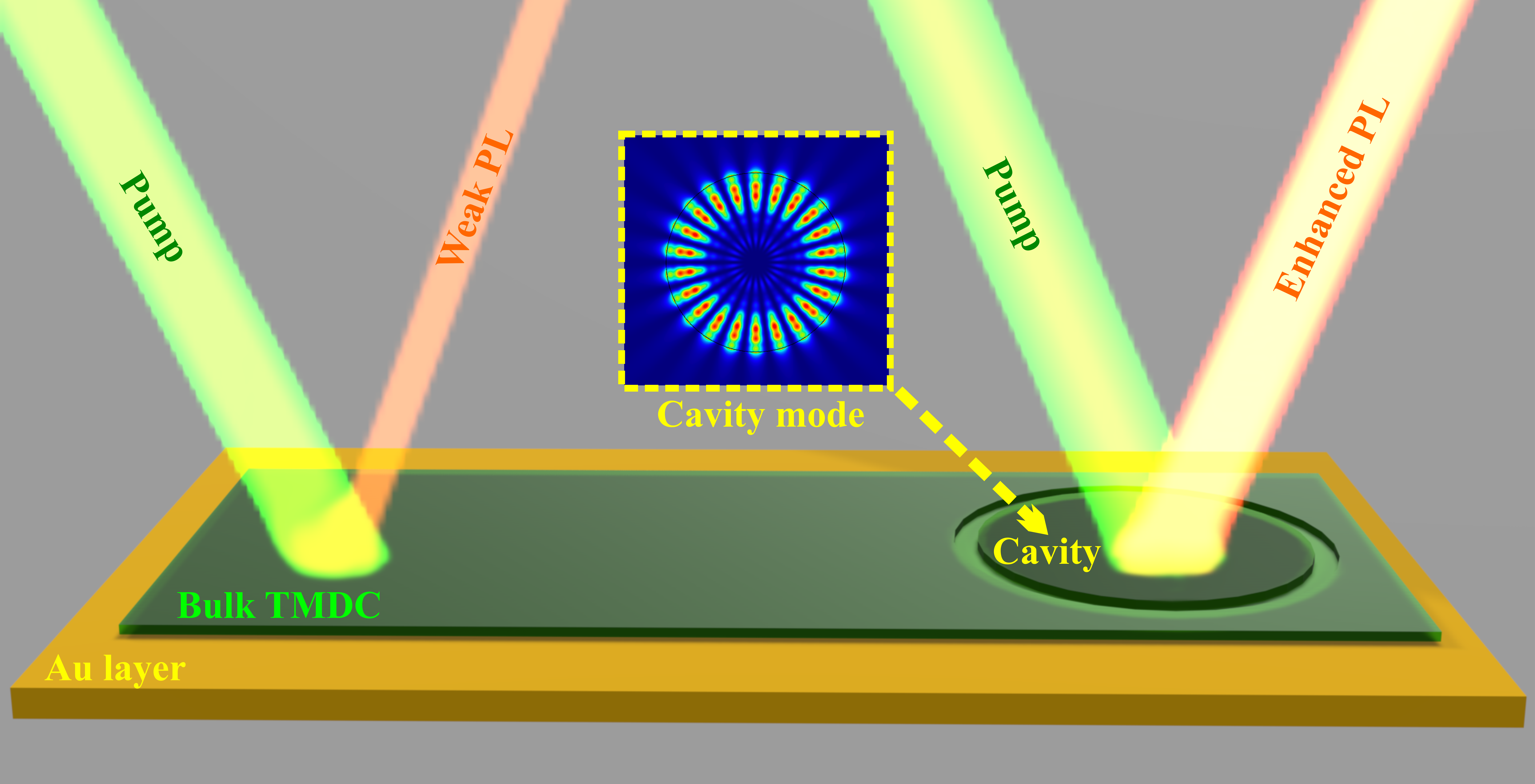
Since the graphene discovery in 20041, layered materials have become one of the most booming topics in many fields, such as materials science2, condensed matter physics3, optoelectronics4, photonics5, etc. The most perspective semiconductive materials seem to be transition metal dichalcogenides (TMDCs). This is due to the unique properties of their monolayers such as extraordinary light absorption6, large exciton binding energy7, 8, strong and tailoring photoluminescence9, 10, 11, the possibility of creating van der Waals heterostructures12, 13, twisting engineering14, 15, 16, etc. Such an active investigation of TMDCs monolayers has revived interest in studying the properties of bulk samples. These materials in their bulk form were actively studied back in the 70s.17, 18, 19, 20 However, today, researchers can take a fresh look at their bulk properties using the progress in understanding physical phenomena and the best modern equipment that allows looking deeper at known properties and finding new ones. Most recent studies revealed many new outstanding properties of multilayered TMDCs, such as giant optical anisotropy21, polarizing effect22, anapole-exciton polaritons23, exciton-plasmon-polaritons24, exciton-polariton transport25, second harmonic generation26, etc. All the above-mentioned make these materials a perfect candidate for a variety of nanophotonic applications including lasers27, 28, waveguides25, 29, 30, high harmonic generation30, 31, 32, bound states in the continuum33, 34, etc. However, there is a significant obstacle in the way of the implementation of light‐emitting nanophotonic devices. Multilayered TMDCs have an indirect bandgap that results in negligible photoluminescence (PL)35. To use some of the unique properties of TMDCs, many researchers integrate direct bandgap TMDC monolayers into external photonic circuits/resonators as a source of excitonic photoluminescence36, 37, 27. However, because of the thickness, monolayers can not accommodate either waveguide or resonant modes in the visible and near-IR ranges. That requires forming photonic circuits and exciton/PL sources using various technological processes and different materials. All this considerably complicates the on-chip integration of TMDCs materials. Another way to solve this problem is to use the Purcell effect to enhance PL intensity of multilayered TMDCs38, 39. This approach was successfully used to enhance light emission of Si in optical cavities40, 41, 42, 43. Although due to strong free charge carriers absorption in Si, the effect was not game-changing44, 45, 46, 47. Owing to an extremely high refractive index in the visible and near-IR ranges (n )48, 49, high-Q nanocavities with a strong Purcell effect and enhanced emissivity might be made from bulk TMDCs (the principle is illustrated in Figure 1).
In this work, we create disk whispering-gallery mode (WGM) optical nanoresonators from multilayered MoSe2. Resistless mechanical probe lithography was used to fabricate nanoresonators so as not to disturb the pristine properties of TMDCs, which are highly sensitive to any contamination or chemical treatment50, 51, 52. The obtained nanocavities demonstrate strongly enhanced (by two orders of magnitude) photoluminescence in the range from 850 to 1050 nm. The spectral features correspond to WGM resonances, which were confirmed by numerical simulations and scattering experiments. The results of the work allow introducing a novel type of stand alone TMDCs nano- and microcavities as a source of excitonic photoluminescence for on-chip integrated nanophotonic circuits.
2 Results and Discussion
2.1 Fabrication of nanocavities
An experimental structure consisted of thin MoSe2 flakes transferred on a Si substrate covered with 50 nm of gold. MoSe2 flakes were obtained by micro-mechanical exfoliation and transferred using a standard approach (i.e., scotch-tape method) without using PDMS to prevent contamination with the polymer51. This process is detailed in Methods. Figure 2a shows the cross-section of the structure used.
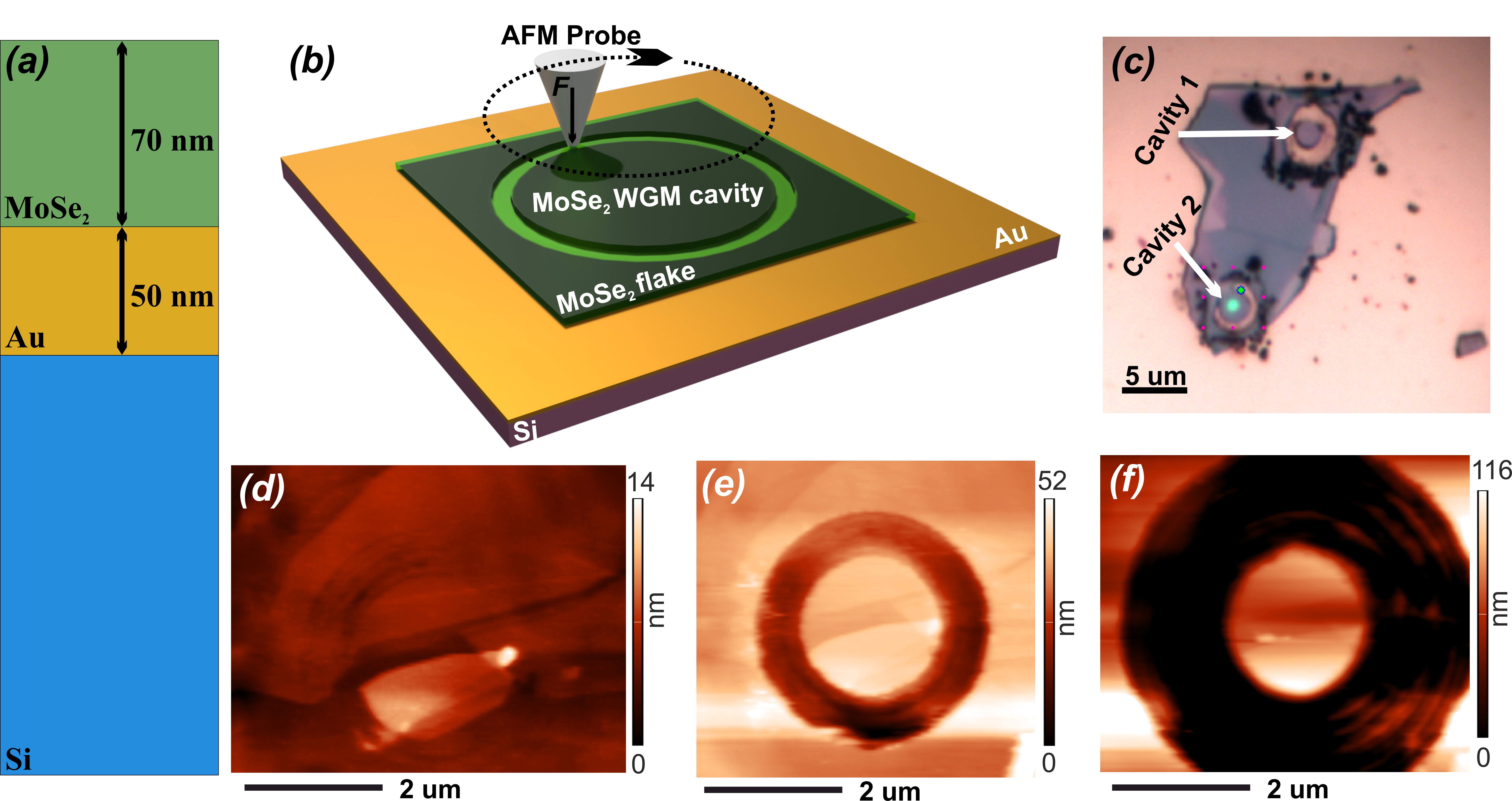
To create a cavity, we firstly found a flake of a thickness about 70-100 nm that is sufficient to accommodate the WGMs. Then we used a frictional scanning probe lithography (f-SPL) to fabricate the cavities53. The scheme of f-SPL is shown in Figure 2b. f-SPL is a resistless method of lithography based on the mechanical influence of an atomic force microscopy (AFM) probe on the sample surface to remove the material (mechanical-SPL). However, while m-SPL conventionally uses high pressure to deepen lithographic patterns (”cutting” regime), f-SPL consists in consequent repetitions of lithographic patterns with small pressure on the sample. Thus, during f-SPL, the material is gradually rubbed out from the surface. This approach allows avoiding the cantilever twisting that prevents the formation of artifacts and makes it possible to maintain high resolution even in the case of thick samples (detailed in Methods). Figure 2c shows an optical image of the processed flake. It can be seen that two circular cavities are formed from the flake, and the removed material is nearby. Figure 2d-f demonstrates AFM images of the cavity creation process. The first is a relatively flat surface of the flake. The second is the surface with a half-thickness trench. The third is the fully separated cavity and the full-thickness trench. The optical properties of such cavities were studied by -PL and dark-field spectroscopy.
2.2 Optical properties of nanocavities
As discussed in the Introduction, TMDs have many peculiar properties that can appear in the optical response of such structures. However, a combination of photoluminescence and scattering investigations is a reliable instrument to determine the nature of observed features. The shape of spectra and peak-to-peak distance are strong evidence of resonant phenomena, whether WGM or Mie resonances. Thus, the optical properties of the cavities were studied using micro-PL and dark-field spectroscopy. Figure 3 demonstrates the results of the PL and experimental dark-field (DF) spectroscopy measurements supported by DF numerical calculations. In the -PL spectrum, we observe a series of peaks (see Figure 3a), which potentially may originate from the whispering gallery mode resonance. Further, we carry out the DF spectroscopy of the cavity previously exposed by PL measurements. Since the DF spectroscopy deals only with optical resonances of a cavity, it allows to unambiguously identify whether PL peaks have the resonant nature or not. The results are shown in Figure 3(b, red curve). One can see that we observe the resonant features in the spectral regions similar to that we get through PL measurements (Figure 3a).
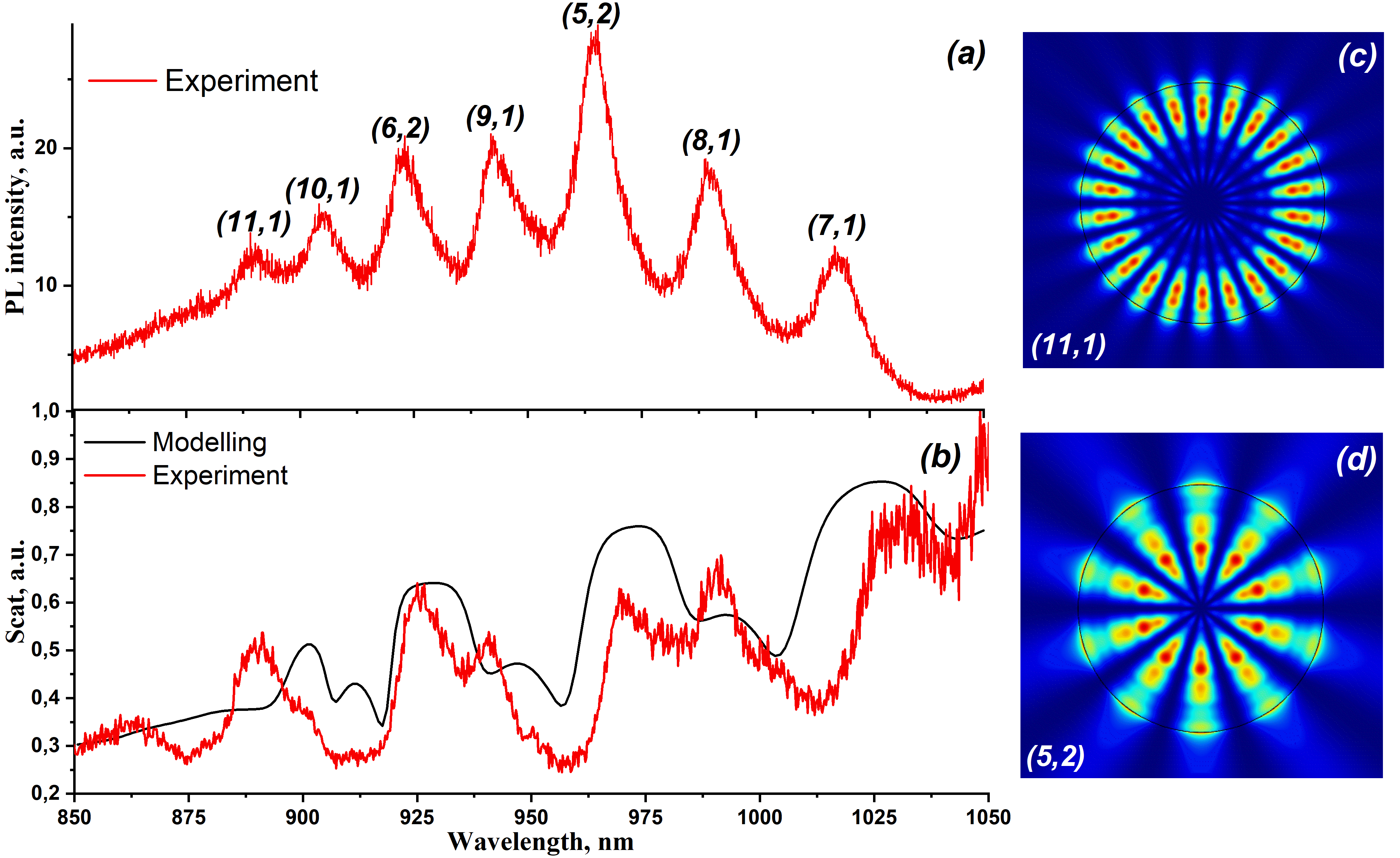
To prove the optical resonance nature of the PL peaks, we prepare comprehensive numerical simulations of optical scattering in COMSOL Multiphysics. We assume a MoSe2 disk on the top of a Si substrate covered by a layer of Au. The permittivities of MoSe2, Si and Au are taken from refs. 54, 18, 55. The disk diameter is 2.2 m, the height is 70 nm, and the thickness of the Au layer is 50 nm. To calculate the scattering spectrum, we illuminate the structure by the s-polarised plane wave with the incident angle of 650 and collect the scattered wave in the numerical aperture of 0.65. The results of the numerical calculation of the DF spectrum are presented in Figure 3(b, black curve). The experimentally obtained DF spectrum is in a good agreement with the numerical one. Based on the resonant behaviour of the DF spectra and peak-to-peak comparison, we conclude that the PL peaks have the optical resonance nature. Figures 3c-d demonstrate electrical field distribution in the cavity for (11, 1) and (5, 2) modes modeled in COMSOL Multiphysics.
Conventionally, when TMDs monolayers are used as light emitters, the external resonator is tuned to the direct exciton transition56, 57, 58 (i.e., 780 nm/1.57 eV in the MoSe2 case)9. In our case, we use a bulk TMD layer simultaneously as a resonator and emitter. Therefore, the absorption of the emitted light is of great importance in our case. Even bulk TMDs have a strong absorbance near the excitonic resonance, while the luminescence is weak19, 59. Thus, to avoid maximum absorption, we should tune our resonators to the long wavelength tail of photoluminescence.
Figure 4 shows the -PL data for cavities of various diameters. The spectra consist of a series of peaks specific for whispering gallery modes. Size variety of the cavities provides different positions of the maxima and enhancement factors. The 2.2 m diameter cavity exhibits significantly enhanced PL with an enhancement factor of up to 100. Additionally, one can notice that the PL maxima of the cavities are shifted to the long-wavelength region comparing to the PL peak of the flake. Such a red-shift of the PL maxima can be explained by the dominant contribution of the cavity modes to the PL in the long-wavelength region (900-1050 nm) and suppression of the cavity radiation due to the significant MoSe2 material losses in the short-wavelength region (800-900 nm). The PL maximum of the bare MoSe2 appears in the highly absorptive wavelength range below 900 nm. Therefore, the cavity modes produce a small PL signal in the short-wavelength region where the absorptive losses are simultaneously resonantly enhanced. For this reason, the disks with smaller diameters of 1.4 and 1.6 m having a high-Q resonances at the shorter wavelengths did not show such a strong enhancement60. Moreover, we created structures of larger diameters (3, 5, and 10 m). The PL data of these structures are presented in Supplementary Information in Figure S1. The 3 m cavity demonstrates some features related to WGMs.
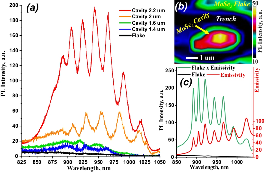
However, these peaks are significantly weaker than in the 2.2 m cavity case, and the flake-like PL peak dominates (see Figure 1S, red curve). With increasing cavity diameter, all WGM features disappear, and only the unmodified flake photoluminescence remains in spectra (see Figure S1, purple and blue curves). Such dependence of PL on cavity diameter can be explained by competition between the gain and material losses. On one hand, a larger cavity should provide higher enhancement due to the high-quality factor of modes with a higher azimuthal number. On the other hand, a longer light path in larger cavities relates to more intensive absorption by indirect bandgap material. Consequently, small cavities have low Q factor but low losses (1.4 and 1.6 m), large cavities have high Q factor but high losses (3, 5, and 10 m), and there is most likely some compromise with satisfying gain and losses (2, and 2.2 m). Thus, we believe that the 2.2 m diameter cavity is a compromise between miniature size and enhancement factor ( ).
The enhanced PL originates from the Purcell effect caused by the whispering gallery modes of the microdisk. The direct measurement of the Purcell factor through time-resolved PL is impeded due to the short (less than 1 ns) lifetime of excited states (see Figure 3S in Supplementary Information). To estimate an impact of the Purcell effect and validate our experimental results, we perform numerical calculations of emissivity of the microdisk in COMSOL Multiphysics61. In order to calculate intensity of the emitted field, we utilize the reciprocity theorem. The reciprocity theorem dictates that the electric field intensity emitted by the current distribution is equal to the intensity necessary for excitation of the this current distribution. As a consequence, the ability of the cavity to absorb the incident energy matches with its ability to emit. Thus, to estimate the emissivity, it is enough to find the energy absorbed in the microdisk. Figure 4(c, red curve) shows the emissivity spectrum of the microdisk with the diameter equal to 2.2 m. The emissivity is calculated as an integral of the field intensity inside the microdisk. Multiplication of the emissivity and the flake PL spectrum gives the PL of the MoSe2 microdisk. The positions of the peaks obtained in the calculations perfectly match with those are experimentally measured.
One can notice that conventionally WGM resonators do not emit vertically. However, the presence of defects might serve as a scatterer or antenna, and a finite aperture of the collecting objective provides simultaneous collection in some angle range. We can see such defects in our structures (e.g., non-uniform thickness in Fig. 2d). In addition, we have noticed that the PL signals strongly depend on a collection spot. Figure 4b demonstrates the PL mapping of one of the structures. It can be seen that the PL intensity is not uniformly distributed, and there are hot spots. So, in our experiments, we chose the spots demonstrating the maximum PL intensity to record the PL spectra.
The nature of PL of such multilayer TMDCs structures is still ambiguous. However, many works point out the optical activity of both direct and indirect transitions in multilayered TMDs62, 63, 64, 65. The common conclusion is that temperature plays a key role in the activation of an indirect transition. In our case, at room temperature, we have a broad PL spectrum modified by a WGM resonator; therefore, its analysis is nontrivial. For this reason, we investigated the temperature dependence of PL for our structures. The results of the investigation are shown in Figure 5.
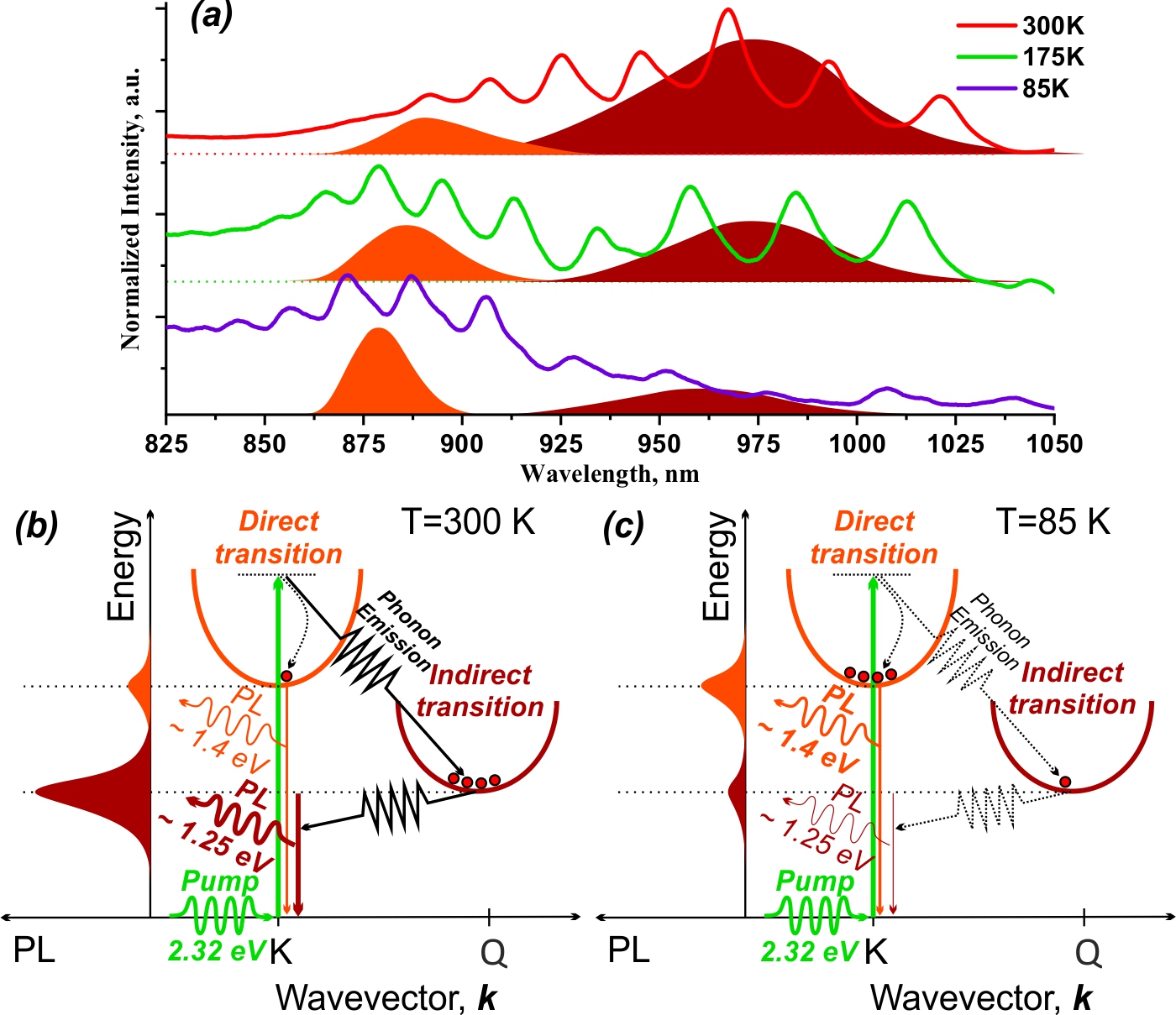
As you can see from Figure 5a, with the decreasing temperature, the broad spectrum at 300 K (see red line) splits into two components at 175 K (see green line), and finally, at 85 K (see violet line), the long-wavelength peak quenches, and short-wavelength one becomes dominant in the spectrum. Based on such behavior of PL, we can assume that observed PL consists of two near peaks. The direct transition is about 1.4 eV, and the indirect transition is about 1.25 eV. The energy of excitation is much higher than both of these (i.e., excitation is non-resonant). Therefore, at room temperature, most of the excited electrons experience phonon-assisted relaxation to the lowest energy state. There, electrons commit radiative phonon-assisted recombination that provides the peak at 1.25 eV. Although, some electrons relax directly to a higher energy state that has a shorter lifetime (i.e., higher oscillator strength) and recombine directly without a phonon that provides the peak at 1.4 eV. This case is illustrated in Figure 5b that corresponds to the spectrum at 300 K (see Fig. 5a). With decreasing temperature, the PL peaks become narrow, and phonons start to freeze out that reduces the effectiveness of the phonon-assisted recombination channel. As a consequence, we can see the separation of direct and indirect peaks and the formation of a ”trough” at 930 nm between them (see Fig. 5a, 175 K). At 85 K, phonons are almost frozen out, and the phonon-assisted channel is ineffective. Therefore, the indirect peak barely can be seen, and the direct channel becomes dominant. This case is illustrated in Figure 5c that corresponds to the spectrum at 85 K (see Fig. 5a). Although, as discussed earlier, the cavities enhance mainly the tails of the PL peaks. So, the actual energies of transitions are probably slightly higher than those we observe here.
3 Conclusions
To conclude, we investigated the optical properties of nanophotonic WGM disk resonators. The resonators were fabricated from bulk indirect bandgap MoSe2 via resistless mechanical scanning probe lithography. The diameter of cavities varied from 1.4 to 10 m, and the thickness was 70 nm. Micro-photoluminescence investigation revealed WGM-like PL spectra with various enhancement factors depending on the cavity diameter. It was shown that the optimal cavity diameter is 2.2 m, which provides enhancement factor of compared to the pristine flake. Scattering experiments and modeling also revealed WGM spectra and confirmed data obtained by micro-PL. Moreover, we investigated the temperature dependence of a cavity PL. The results showed that PL has two components - the short-wavelength ( nm) and the long-wavelength ( nm). With decreasing temperature, the long-wavelength component quenches, while the short-wavelength one becomes dominant. Based on it, we assume that two transitions are simultaneously active in our structures PL - direct ( eV) and indirect ( eV).
Thus, in this work, we demonstrated a novel approach to the fabrication of light-emitting nanophotonic devices based on bulk indirect bandgap TMDs and investigated the optical properties of several. We believe that this approach might be promising to create other light-emitting nanophotonic devices from bulk TMDs and reveal their fascinating properties.
4 Methods
Sample preparation. Thin-film MoSe2 samples were fabricated by mechanical exfoliation with adhesive tape (blue tape, Nitto) from a commercial bulk crystal (obtained from HQ Graphene, Netherland) on top of the Au/Si substrate.
Cavities creation. The cavities were created by resistless frictional mechanical probe lithography. To perform the procedure, we used Ntegra Aura (NT-MDT) atomic force microscope using DCP (NT-MDT) probes with a curvature radius of 100 nm and a spring constant of 30-85 N/m. The multi-pass frictional approach was used to prevent defect formation. The force was about 10 uN, and number of passes amounted to 200 for each resonator. Detailed information on this approach and the cavity creation process is available in our previous works.60, 53
Micro-photoluminescence (-PL) investigation. The optical properties of the structures were investigated by measuring the PL spectra. For these experiments, a multi-functional optical complex Horiba LabRAM HREvo UV-VIS-NIR-Open equipped with a confocal microscope was used. Spectra were obtained with a spectral resolution of 3 cm-1 using a 600 gr/mm grating. We used an Olympus MPLN100 objective lens (NA = 0.9) to obtain information from an area with a diameter of 1 m. Apart from local measurements, PL mapping with spatial resolution of 0.5 m was performed at the same setup using a motorized table. The measurements were performed with continuous-wave (cw) excitation using the 532 nm laser line of a Nd:YAG laser (Laser Quantum Torus). To prevent damage to the structures, the incident laser power was limited to 1 mW.
Scattering experiments. The microdisks were illuminated with white polarised light (Ocean Optics HL-2000-HP in combination with linear polariser) at an incidence angle of 65 degrees with a low-aperture lens Mitutoyo Plan Apo NIR 10x 0.26 NA. The radiation scattered by the disks is collected using the Mitutoyo Plan Apo NIR 50x 0.65 NA which was analysed on a Horiba LabRAM HR 800 UV-VIS-NIR spectrometer. The numerical apertures of the lenses and the angle of incidence are chosen so that pump not pass through the collection channel.
There is no funding to report.
We thank Mikhail M. Glazov and Ivan V. Iorsh for fruitful discussions.
References
- Novoselov et al. 2004 Novoselov, K. S.; Geim, A. K.; Morozov, S. V.; Jiang, D.-e.; Zhang, Y.; Dubonos, S. V.; Grigorieva, I. V.; Firsov, A. A. Electric field effect in atomically thin carbon films. science 2004, 306, 666–669
- Manzeli et al. 2017 Manzeli, S.; Ovchinnikov, D.; Pasquier, D.; Yazyev, O. V.; Kis, A. 2D transition metal dichalcogenides. Nature Reviews Materials 2017, 2, 1–15
- Kennes et al. 2021 Kennes, D. M.; Claassen, M.; Xian, L.; Georges, A.; Millis, A. J.; Hone, J.; Dean, C. R.; Basov, D.; Pasupathy, A. N.; Rubio, A. Moiré heterostructures as a condensed-matter quantum simulator. Nature Physics 2021, 17, 155–163
- Jing et al. 2020 Jing, Y.; Liu, B.; Zhu, X.; Ouyang, F.; Sun, J.; Zhou, Y. Tunable electronic structure of two-dimensional transition metal chalcogenides for optoelectronic applications. Nanophotonics 2020, 9, 1675–1694
- Mak and Shan 2016 Mak, K. F.; Shan, J. Photonics and optoelectronics of 2D semiconductor transition metal dichalcogenides. Nature Photonics 2016, 10, 216–226
- Bernardi et al. 2013 Bernardi, M.; Palummo, M.; Grossman, J. C. Extraordinary sunlight absorption and one nanometer thick photovoltaics using two-dimensional monolayer materials. Nano letters 2013, 13, 3664–3670
- Ugeda et al. 2014 Ugeda, M. M.; Bradley, A. J.; Shi, S.-F.; Felipe, H.; Zhang, Y.; Qiu, D. Y.; Ruan, W.; Mo, S.-K.; Hussain, Z.; Shen, Z.-X., et al. Giant bandgap renormalization and excitonic effects in a monolayer transition metal dichalcogenide semiconductor. Nature materials 2014, 13, 1091–1095
- Hanbicki et al. 2015 Hanbicki, A.; Currie, M.; Kioseoglou, G.; Friedman, A.; Jonker, B. Measurement of high exciton binding energy in the monolayer transition-metal dichalcogenides WS2 and WSe2. Solid State Communications 2015, 203, 16–20
- Tonndorf et al. 2013 Tonndorf, P.; Schmidt, R.; Böttger, P.; Zhang, X.; Börner, J.; Liebig, A.; Albrecht, M.; Kloc, C.; Gordan, O.; Zahn, D. R., et al. Photoluminescence emission and Raman response of monolayer MoS 2, MoSe 2, and WSe 2. Optics express 2013, 21, 4908–4916
- Tongay et al. 2013 Tongay, S.; Zhou, J.; Ataca, C.; Liu, J.; Kang, J. S.; Matthews, T. S.; You, L.; Li, J.; Grossman, J. C.; Wu, J. Broad-range modulation of light emission in two-dimensional semiconductors by molecular physisorption gating. Nano letters 2013, 13, 2831–2836
- Benimetskiy et al. 2019 Benimetskiy, F.; Sharov, V.; Alekseev, P.; Kravtsov, V.; Agapev, K.; Sinev, I.; Mukhin, I.; Catanzaro, A.; Polozkov, R.; Alexeev, E., et al. Measurement of local optomechanical properties of a direct bandgap 2D semiconductor. APL Materials 2019, 7, 101126
- Geim and Grigorieva 2013 Geim, A. K.; Grigorieva, I. V. Van der Waals heterostructures. Nature 2013, 499, 419–425
- Fan et al. 2020 Fan, S.; Vu, Q. A.; Tran, M. D.; Adhikari, S.; Lee, Y. H. Transfer assembly for two-dimensional van der Waals heterostructures. 2D Materials 2020, 7, 022005
- Michl et al. 2021 Michl, J.; Tarasenko, S.; Lohof, F.; Gies, G.; von Helversen, M.; Sailus, R.; Tongay, S.; Taniguchi, T.; Watanabe, K.; Heindel, T., et al. Intrinsic circularly-polarized exciton emission in a twisted van-der-Waals heterostructure. arXiv preprint arXiv:2105.09948 2021,
- Tran et al. 2020 Tran, K.; Choi, J.; Singh, A. Moiré and beyond in transition metal dichalcogenide twisted bilayers. 2D Materials 2020,
- Shabani et al. 2021 Shabani, S.; Halbertal, D.; Wu, W.; Chen, M.; Liu, S.; Hone, J.; Yao, W.; Basov, D. N.; Zhu, X.; Pasupathy, A. N. Deep moiré potentials in twisted transition metal dichalcogenide bilayers. Nature Physics 2021, 17, 720–725
- Goldberg et al. 1975 Goldberg, A.; Beal, A.; Levy, F.; Davis, E. The low-energy absorption edge in 2H-MoS2 and 2H-MoSe2. Philosophical Magazine 1975, 32, 367–378
- Beal and Hughes 1979 Beal, A.; Hughes, H. Kramers-Kronig analysis of the reflectivity spectra of 2H-MoS2, 2H-MoSe2 and 2H-MoTe2. Journal of Physics C: Solid State Physics 1979, 12, 881
- Wilson and Yoffe 1969 Wilson, J. A.; Yoffe, A. The transition metal dichalcogenides discussion and interpretation of the observed optical, electrical and structural properties. Advances in Physics 1969, 18, 193–335
- Anedda and Fortin 1980 Anedda, A.; Fortin, E. Exciton spectra in MoSe2. Journal of Physics and Chemistry of Solids 1980, 41, 865–869
- Ermolaev et al. 2021 Ermolaev, G.; Grudinin, D.; Stebunov, Y.; Voronin, K. V.; Kravets, V.; Duan, J.; Mazitov, A.; Tselikov, G.; Bylinkin, A.; Yakubovsky, D., et al. Giant optical anisotropy in transition metal dichalcogenides for next-generation photonics. Nature communications 2021, 12, 1–8
- Berahim et al. 2019 Berahim, N.; Amiri, I. S.; Anwar, T.; Azzuhri, S. R.; Nasir, M. M.; Zakaria, R.; Chong, W. Y.; Lai, C. K.; Lee, S. H.; Ahmad, H., et al. Polarizing effect of MoSe2-coated optical waveguides. Results in Physics 2019, 12, 7–11
- Verre et al. 2019 Verre, R.; Baranov, D. G.; Munkhbat, B.; Cuadra, J.; Käll, M.; Shegai, T. Transition metal dichalcogenide nanodisks as high-index dielectric Mie nanoresonators. Nature nanotechnology 2019, 14, 679–683
- Zhang et al. 2020 Zhang, H.; Abhiraman, B.; Zhang, Q.; Miao, J.; Jo, K.; Roccasecca, S.; Knight, M. W.; Davoyan, A. R.; Jariwala, D. Hybrid exciton-plasmon-polaritons in van der Waals semiconductor gratings. Nature communications 2020, 11, 1–9
- Hu et al. 2017 Hu, F.; Luan, Y.; Scott, M.; Yan, J.; Mandrus, D.; Xu, X.; Fei, Z. Imaging exciton–polariton transport in MoSe 2 waveguides. Nature Photonics 2017, 11, 356–360
- Busschaert et al. 2020 Busschaert, S.; Reimann, R.; Cavigelli, M.; Khelifa, R.; Jain, A.; Novotny, L. Transition metal dichalcogenide resonators for second harmonic signal enhancement. ACS Photonics 2020, 7, 2482–2488
- Ye et al. 2015 Ye, Y.; Wong, Z. J.; Lu, X.; Ni, X.; Zhu, H.; Chen, X.; Wang, Y.; Zhang, X. Monolayer excitonic laser. Nature Photonics 2015, 9, 733–737
- Li et al. 2017 Li, Y.; Zhang, J.; Huang, D.; Sun, H.; Fan, F.; Feng, J.; Wang, Z.; Ning, C.-Z. Room-temperature continuous-wave lasing from monolayer molybdenum ditelluride integrated with a silicon nanobeam cavity. Nature nanotechnology 2017, 12, 987–992
- Fei et al. 2016 Fei, Z.; Scott, M.; Gosztola, D.; Foley IV, J.; Yan, J.; Mandrus, D.; Wen, H.; Zhou, P.; Zhang, D.; Sun, Y., et al. Nano-optical imaging of WS e 2 waveguide modes revealing light-exciton interactions. Physical Review B 2016, 94, 081402
- Munkhbat et al. 2022 Munkhbat, B.; Küçüköz, B.; Baranov, D. G.; Antosiewicz, T. J.; Shegai, T. O. Nanostructured transition metal dichalcogenide multilayers for advanced nanophotonics. arXiv preprint arXiv:2202.04898 2022,
- Khan et al. 2022 Khan, A. R.; Zhang, L.; Ishfaq, K.; Ikram, A.; Yildrim, T.; Liu, B.; Rahman, S.; Lu, Y. Optical Harmonic Generation in 2D Materials. Advanced Functional Materials 2022, 32, 2105259
- Autere et al. 2018 Autere, A.; Jussila, H.; Dai, Y.; Wang, Y.; Lipsanen, H.; Sun, Z. Nonlinear optics with 2D layered materials. Advanced Materials 2018, 30, 1705963
- Muhammad et al. 2021 Muhammad, N.; Chen, Y.; Qiu, C.-W.; Wang, G. P. Optical bound states in continuum in MoS2-based metasurface for directional light emission. Nano Letters 2021, 21, 967–972
- Bernhardt et al. 2020 Bernhardt, N.; Koshelev, K.; White, S. J.; Meng, K. W. C.; Froch, J. E.; Kim, S.; Tran, T. T.; Choi, D.-Y.; Kivshar, Y.; Solntsev, A. S. Quasi-BIC resonant enhancement of second-harmonic generation in WS2 monolayers. Nano Letters 2020, 20, 5309–5314
- Tongay et al. 2012 Tongay, S.; Zhou, J.; Ataca, C.; Lo, K.; Matthews, T. S.; Li, J.; Grossman, J. C.; Wu, J. Thermally driven crossover from indirect toward direct bandgap in 2D semiconductors: MoSe2 versus MoS2. Nano letters 2012, 12, 5576–5580
- Wang et al. 2019 Wang, L.; Zhou, X.; Yang, S.; Huang, G.; Mei, Y. 2D-material-integrated whispering-gallery-mode microcavity. Photonics Research 2019, 7, 905–916
- Krasnok et al. 2018 Krasnok, A.; Lepeshov, S.; Alú, A. Nanophotonics with 2D transition metal dichalcogenides. Optics express 2018, 26, 15972–15994
- Purcell 1995 Purcell, E. M. Confined Electrons and Photons; Springer, 1995; pp 839–839
- Eswaramoorthy et al. 2021 Eswaramoorthy, L.; Mokkapati, S.; Kumar, A. Engineering Purcell factor anisotropy for dark and bright excitons in two dimensional semiconductors. arXiv preprint arXiv:2108.10680 2021,
- Cho et al. 2013 Cho, C.-H.; Aspetti, C. O.; Park, J.; Agarwal, R. Silicon coupled with plasmon nanocavities generates bright visible hot luminescence. Nature photonics 2013, 7, 285–289
- Fujita 2013 Fujita, M. Nanocavity brightens silicon. Nature Photonics 2013, 7, 264–265
- Valenta et al. 2019 Valenta, J.; Greben, M.; Dyakov, S.; Gippius, N.; Hiller, D.; Gutsch, S.; Zacharias, M. Nearly perfect near-infrared luminescence efficiency of Si nanocrystals: A comprehensive quantum yield study employing the Purcell effect. Scientific reports 2019, 9, 1–9
- Gong et al. 2010 Gong, Y.; Ishikawa, S.; Cheng, S.-L.; Gunji, M.; Nishi, Y.; Vučković, J. Photoluminescence from silicon dioxide photonic crystal cavities with embedded silicon nanocrystals. Physical Review B 2010, 81, 235317
- Kekatpure and Brongersma 2008 Kekatpure, R. D.; Brongersma, M. L. Quantification of free-carrier absorption in silicon nanocrystals with an optical microcavity. Nano Letters 2008, 8, 3787–3793
- Fauchet 1998 Fauchet, P. M. The integration of nanoscale porous silicon light emitters: materials science, properties, and integration with electronic circuitry. Journal of luminescence 1998, 80, 53–64
- Elliman et al. 2007 Elliman, R.; Forcales, M.; Wilkinson, A.; Smith, N. Waveguiding properties of Er-implanted silicon-rich oxides. Nuclear Instruments and Methods in Physics Research Section B: Beam Interactions with Materials and Atoms 2007, 257, 11–14
- Ridley 2013 Ridley, B. K. Quantum processes in semiconductors; Oxford university press, 2013
- Hsu et al. 2019 Hsu, C.; Frisenda, R.; Schmidt, R.; Arora, A.; de Vasconcellos, S. M.; Bratschitsch, R.; van der Zant, H. S.; Castellanos-Gomez, A. Thickness-dependent refractive index of 1L, 2L, and 3L MoS2, MoSe2, WS2, and WSe2. Advanced Optical Materials 2019, 7, 1900239
- Jung et al. 2019 Jung, G.-H.; Yoo, S.; Park, Q.-H. Measuring the optical permittivity of two-dimensional materials without a priori knowledge of electronic transitions. Nanophotonics 2019, 8, 263–270
- Du et al. 2008 Du, X.; Skachko, I.; Barker, A.; Andrei, E. Y. Approaching ballistic transport in suspended graphene. Nature nanotechnology 2008, 3, 491–495
- Schwartz et al. 2019 Schwartz, J. J.; Chuang, H.-J.; Rosenberger, M. R.; Sivaram, S. V.; McCreary, K. M.; Jonker, B. T.; Centrone, A. Chemical identification of interlayer contaminants within van der Waals heterostructures. ACS applied materials & interfaces 2019, 11, 25578–25585
- Garcia et al. 2014 Garcia, R.; Knoll, A. W.; Riedo, E. Advanced scanning probe lithography. Nature nanotechnology 2014, 9, 577–587
- Borodin et al. 2021 Borodin, B.; Benimetskiy, F.; Alekseev, P. Mechanical frictional scanning probe lithography of TMDCs. Journal of Physics: Conference Series. 2021; p 012090
- Schinke et al. 2015 Schinke, C.; Christian Peest, P.; Schmidt, J.; Brendel, R.; Bothe, K.; Vogt, M. R.; Kröger, I.; Winter, S.; Schirmacher, A.; Lim, S., et al. Uncertainty analysis for the coefficient of band-to-band absorption of crystalline silicon. AIP Advances 2015, 5, 067168
- Johnson and Christy 1972 Johnson, P. B.; Christy, R.-W. Optical constants of the noble metals. Physical review B 1972, 6, 4370
- Ardizzone et al. 2019 Ardizzone, V.; De Marco, L.; De Giorgi, M.; Dominici, L.; Ballarini, D.; Sanvitto, D. Emerging 2D materials for room-temperature polaritonics. Nanophotonics 2019, 8, 1547–1558
- Li et al. 2021 Li, M.; Sinev, I.; Benimetskiy, F.; Ivanova, T.; Khestanova, E.; Kiriushechkina, S.; Vakulenko, A.; Guddala, S.; Skolnick, M.; Menon, V. M., et al. Experimental observation of topological Z2 exciton-polaritons in transition metal dichalcogenide monolayers. Nature communications 2021, 12, 1–10
- Sinev et al. 2021 Sinev, I.; Li, M.; Benimetskiy, F.; Ivanova, T.; Kiriushechkina, S.; Vakulenko, A.; Guddala, S.; Krizhanovskii, D.; Samusev, A.; Khanikaev, A. Strong light-matter coupling in topological metasurfaces integrated with transition metal dichalcogenides. Journal of Physics: Conference Series. 2021; p 012142
- Dong et al. 2015 Dong, N.; Li, Y.; Feng, Y.; Zhang, S.; Zhang, X.; Chang, C.; Fan, J.; Zhang, L.; Wang, J. Optical limiting and theoretical modelling of layered transition metal dichalcogenide nanosheets. Scientific reports 2015, 5, 1–10
- Borodin et al. 2021 Borodin, B.; Benimetskiy, F.; Davydov, V. Y.; Eliseyev, I.; Lepeshov, S.; Bogdanov, A.; Alekseev, P. Mechanical scanning probe lithography of nanophotonic devices based on multilayer TMDCs. Journal of Physics: Conference Series. 2021; p 012020
- Dyakov et al. 2021 Dyakov, S. A.; Stepikhova, M. V.; Bogdanov, A. A.; Novikov, A. V.; Yurasov, D. V.; Shaleev, M. V.; Krasilnik, Z. F.; Tikhodeev, S. G.; Gippius, N. A. Photonic bound states in the continuum in Si structures with the self-assembled Ge nanoislands. Laser & Photonics Reviews 2021, 15, 2000242
- Shubina et al. 2019 Shubina, T. V.; Remškar, M.; Davydov, V. Y.; Belyaev, K. G.; Toropov, A. A.; Gil, B. Excitonic emission in van der Waals nanotubes of transition metal dichalcogenides. Annalen der Physik 2019, 531, 1800415
- Malic et al. 2018 Malic, E.; Selig, M.; Feierabend, M.; Brem, S.; Christiansen, D.; Wendler, F.; Knorr, A.; Berghäuser, G. Dark excitons in transition metal dichalcogenides. Physical Review Materials 2018, 2, 014002
- Smirnova et al. 2020 Smirnova, O.; Eliseyev, I.; Rodina, A.; Shubina, T. Temperature activation of indirect exciton in nanostructures based on MoS2. Journal of Physics: Conference Series. 2020; p 012038
- Brem et al. 2020 Brem, S.; Ekman, A.; Christiansen, D.; Katsch, F.; Selig, M.; Robert, C.; Marie, X.; Urbaszek, B.; Knorr, A.; Malic, E. Phonon-assisted photoluminescence from indirect excitons in monolayers of transition-metal dichalcogenides. Nano letters 2020, 20, 2849–2856