Operation of Cs-Sb-O activated GaAs in a high voltage DC electron gun at high average current
Abstract
Negative Electron Affinity (NEA) activated GaAs photocathodes are the most popular option for generating a high current ( 1 mA) spin-polarized electron beam. Despite its popularity, a short operational lifetime is the main drawback of this material. Recent works have shown that the lifetime can be improved by using a robust Cs-Sb-O NEA layer with minimal adverse effects. In this work, we operate GaAs photocathodes with this new activation method in a high voltage environment to extract a high current. We observed spectral dependence on the lifetime improvement. In particular, we saw a 45% increase in the lifetime at 780 nm for Cs-Sb-O activated GaAs compared to Cs-O activated GaAs.
I Introduction
An electron source capable of sustaining high-intensity production of spin-polarized electrons is highly desired for nuclear and high energy physics applications.cardman2018 ; adolphson2011large Furthermore, electron microscopy technologies can utilize spin-polarized electrons to study magnetization in materials and nanostructures.suzuki2010_RealTimeMagnetic ; kuwahara2012_30kVSpinpolarizedTransmission ; vollmer2003 A Negative Electron Affinity (NEA) activated GaAs in a high voltage electron gun is the only viable option to produce a highly spin-polarized electron beam at a high current. However, the extreme vacuum sensitivity of the NEA layer is the main drawback that results in rapid Quantum Efficiency (QE) degradation over time; hence it has a short operational lifetime compared to other types of photocathodes.grames2011_ChargeFluenceLifetime ; bae2018_RuggedSpinpolarizedElectron ; bae2020_ImprovedLifetimeHigh ; cultrera2020_LongLifetimePolarized
Quantum mechanical selection rules in optically stimulated electronic transition must be leveraged to achieve the photoemission of spin-polarized electrons from bulk GaAs.pierce1976 ; liu2017_ComprehensiveEvaluationFactors Using circularly polarized light with photon energy slightly larger than the bandgap, electrons can be excited from the top of the valence band to the bottom of the conduction band with polarization up to a theoretical limit of 50%.pierce1976 Extracting these electrons from the photocathode requires a vacuum interface with NEA condition. As in bulk GaAs, most layered GaAs-based photocathodes can be designed to achieve a sufficiently large QE and high electron spin polarization when excited with wavelengths close to 780 nm.liu2016_RecordlevelQuantumEfficiency Therefore, the operational lifetime at 780 nm is crucial for large accelerator facilities applications.
Three main mechanisms are responsible for the rapid degradation of QE: ion back-bombardment,grames2011_ChargeFluenceLifetime ; cultrera2011_PhotocathodeBehaviorHigh ; liu2016_EffectsIonBombardmenta chemical poisoning,chanlek2014_DegradationQuantumEfficiency and thermal desorption of the activation layer.kuriki2011_DarklifetimeDegradationGaAs Ion back-bombardment occurs when the electron beam ionizes the residual gases in the vacuum. The positively charged ions are accelerated towards the cathode and degrade the cathode performance.grames2011_ChargeFluenceLifetime ; cultrera2011_PhotocathodeBehaviorHigh Chemical poisoning of the cathode happens as the NEA activation layer chemically reacts with the residual gases in the vacuum.chanlek2014_DegradationQuantumEfficiency As ion back-bombardment and chemical poisoning degrade the QE during beam operation, a higher laser intensity is required to maintain the beam current at the same level, and the increased laser power might further accelerate the thermal desorption of the NEA layer. Among the three mechanisms, the ion back-bombardment is considered the most significant contributor to performance degradation during high current operations. It has been shown that such a process can be minimized by extracting electrons a few mm off from the electrostatic center, limiting the photocathode active area, increasing the laser spot size, and applying a positive bias to the anode.grames2011_ChargeFluenceLifetime ; yoskowitz2021_IMPROVINGOPERATIONALLIFETIME
Ion back bombardment can degrade QE by three different processes. High energy ions ( 5 keV) can interact with lattice atoms and create vacancies, directly damaging the GaAs structure.biswas2019_StudyPhotocathodeSurfacea ; liu2016_EffectsIonBombardmenta Lower energy ions ( 500 eV) can penetrate the cathode surface and create interstitial defects near the vacuum interface. These defects will affect the diffusion length of electrons and hence lower the escape probability of photoelectrons.liu2016_EffectsIonBombardmenta The last possibility is that ions between 500 eV and 5 keV can interact with atoms on the surface and remove the NEA activation layer via sputtering.biswas2019_StudyPhotocathodeSurfacea The QE degradation is expected to be a convolution of these three processes, but the relative contribution of each is not well understood and left to be explored. Understanding the convolution would be critical to potential mitigation.
Traditional NEA activation layers such as Cs-O2 and Cs-NF3 form a submonolayer that is chemically reactive and weakly bound to the surface.kuriki2011_DarklifetimeDegradationGaAs ; chanlek2014_DegradationQuantumEfficiency A study found that using two alkali species, Cs and Li, for NEA activation could improve the chemical stability of GaAs photocathode under CO2 exposure.mulhollan2008_EnhancedChemicalImmunity ; sun2009_SurfaceActivationLayer ; kurichiyanil2019test Recently, multiple research groups reported significantly improved lifetime using a few nm thick semiconductor activation layer with elements that form more robust photocathodes, such as Cs, Sb, Te, O.kuriki2019_NegativeElectronAffinity ; biswas2021_HighQuantumEfficiency ; rahman2019_NewActivationTechniques We reported a factor of 5 improvements in charge lifetime at 532 nm wavelength with Cs-Te activation layerbae2018_RuggedSpinpolarizedElectron and a factor of 7 improvements at 780 nm with Cs-Sb-O layer.bae2020_ImprovedLifetimeHigh Moreover, these layers showed a minimal adverse effect on spin-polarization.bae2018_RuggedSpinpolarizedElectron ; bae2020_ImprovedLifetimeHigh ; cultrera2020_LongLifetimePolarized However, these photoemission measurements were done with a 10’s of eV bias and 100’s of nA beam current, which is significantly different from the harsh environment of an electron gun that operates on the scale of 100’s of keV. Specifically, the amount of current extracted and the energy-dependent residual gas ionization cross-sections are orders of magnitude different.grames2011_ChargeFluenceLifetime Furthermore, the primary QE degradation mechanism was chemical poisoning in our previous works as opposed to ion back bombardment.cultrera2020_LongLifetimePolarized In this work, we operated Cs-Sb-O and Cs-O activated GaAs photocathodes in the High ElectRon Average Current for Lifetime ExperimentS (HERACLES) beamline at Cornell University in order to make a direct comparison of their performance at 200 keV beam energy at 1 mA average current. We saw a spectral dependence on lifetime improvement between the two types of samples and observed 45% improvement in charge lifetime at 780 nm.
II Growth
Highly p-doped (Zn cm-3) GaAs (100) wafers were cleaved in air with a diamond scribe. Cleaved samples were rinsed in de-ionized water and solvent cleaned with isopropanol. We performed wet-etching with 1% HF acid for 30 s, and then the samples were loaded into the vacuum for heat cleaning at C∘ for hours. Cs-O activation was performed in a vacuum chamber directly connected to the back of the electron gun that has a pressure of Torr. Resistively heated dispensers from SAES Getters were used for the Cs source, and O2 was injected with a mechanical leak valve. We activated GaAs samples with the Cs-O2 codeposition method at room temperature.
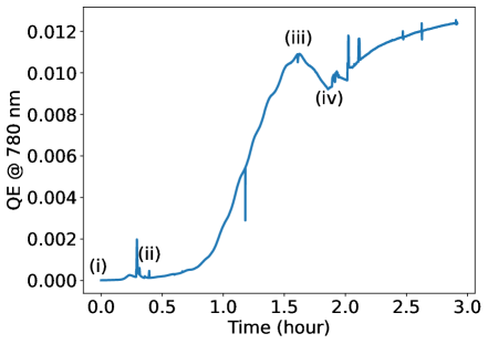
For Cs-Sb-O activation, the growth was performed in a separate vacuum system located in another laboratory, and the cathodes were subsequently transported with a vacuum suitcase. The growth chamber has a pressure of Torr, and single filament effusion cells were installed as Cs and Sb sources. Shutters in front of each source act as an on/off control of the flux. We leaked O2 into the chamber with a mechanical leak valve similar to the Cs-O activation chamber. The temperature of the samples was kept at C∘ during the growth. QE at 780 nm was monitored during the growth with a diode laser ( 10 W) under 18 V negative bias.feng2019_activation Fig. 1 demonstrates the QE at 780 nm during the growth process. (i) Samples were initially activated with just Cs until QE peaks and started decreasing. (ii) As soon as the QE decrease was observed, O2 was leaked into the chamber. (iii) the Sb shutter was opened when QE saturated to a percent level. Cs, Sb, and O2 are all being deposited simultaneously during Sb deposition. (iv) Sb shutter was closed after depositing 0.2 nm. The heater was turned off, the O2 leak valve was closed, and the Cs shutter was closed soon after. The Sb deposition amount and flux ( atoms/cm2/s) were estimated using a quartz crystal microbalance. The decreased QE during Sb deposition recovered while cooling down of the sample. The activated cathodes were transported to the gun using a custom ultrahigh vacuum suitcase that has a base pressure of Torr.galdi2020_EffectsOxygeninducedPhase The suitcase was constantly pumped by a compact 400 l/s non-evaporative getter during the transport, and an 8 l/s ion pump was turned on once it was attached to the load-lock chamber of HERACLES. We typically pumped the load-lock chamber overnight before transporting the cathodes into the gun.
III Instrument
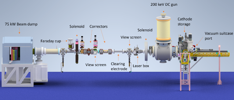
The HERACLES beamline consists of a 200 keV electron gun and a 75 kW beam dump (See Fig. 2). The gun was originally fabricated for the Cornell Electron Recovery Linac (ERL) program. It was used to demonstrate the record highest average current obtained from a photocathode.dunham2013_RecordHighaverageCurrent Recently, the gun, beam dump, and some of the beamline components were moved to the same building as the Cornell Photocathode laboratory to enable an experimental program for producing and testing long-lived photocathodes at high average beam currents. In the current configuration, beyond the gun, the HERACLES beamline comprises two solenoids, three horizontal/vertical corrector pairs, three BeO pneumatically mounted view screens, a faraday cup for low current (100 nA) measurements, an emittance measuring system, and a quadrant detector for beam position monitoring at high currents. The beam dump is composed of 16 chilled water lines that are independently monitored with thermocouples that serve as a further diagnostic during high-current running. The beamline also includes two sets of clearing electrodes to reduce ion-back bombardment.
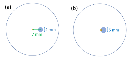
During the high current runs presented in this work, we used Sabre Innova Argon gas laser by Coherent operated in the visible at 488 nm. A 1-to-1 imaging system consisting of a single 750 mm lens is used to image a 1.2 mm diameter pinhole onto the cathode active area. A small portion of the laser light is split off into a diagnostics optics path to allow the power to be monitored during the run. The laser spot was positioned on the 7 mm off-centered active area on the cathode that has 4 mm diameter (see Fig. 3 (a)). Our control system is EPICS-based.dalesio1991epics For running at 100 A or more, the beam current is inferred from the current drawn by the gun power supply. During a charge lifetime measurement, the laser power is adjusted to maintain a constant current via a proportional-integral feedback loop implemented in Python with PYEPICS.
Two vacuum chambers are connected behind the HERACLES gun. The first chamber has a mechanical arm for placing and removing cathodes in the gun, a vacuum attachment port for accepting cathodes via a vacuum suitcase, and has the capacity to store up to three cathodes. The second chamber, dubbed the QE-mapping chamber, has a cesium source and oxygen leak valve to enable Cs-O activation of GaAs. In this chamber, the saddle is electrically isolated and can be negatively biased to allow for photocurrent to be monitored during an activation. Outside this chamber, a diode laser is mounted to a 2D motorized stage to obtain transverse maps of the cathode’s QE (Fig. 5). Such a diagnostic is critical for an examination of the cathode after a high-current run to identify the main driver(s) of the cathode’s performance degradation.
IV Results and Discussion
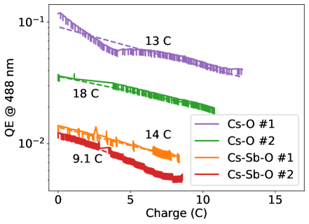
Charge lifetime is defined as the amount of charge extracted until QE drops to 1/e of the initial value.grames2011_ChargeFluenceLifetime ; bae2018_RuggedSpinpolarizedElectron In Fig. 4, QE at 488 nm was monitored during 200 keV operation at 1 mA. We obtained charge lifetimes around 15 C for the reference Cs-O activated GaAs photocathodes. It must be noted that this value is two orders of magnitude lower than the ones achieved at the Thomas-Jefferson lab.grames2011_ChargeFluenceLifetime We believe there are two main reasons. First, the pressure of the DC gun at Cornell is typically around Torr in a standby mode, and it can rise up to Torr during an operation. On the other hand, the electron gun in the Jefferson Lab is operated under mid Torr pressure.grames2011_ChargeFluenceLifetime Secondly, it has been found that a high voltage photogun can produce unwanted photoelectrons from the edge of an active area that is not properly transported away.grames2011_ChargeFluenceLifetime ; sinclair2007_DevelopmentHighAverage These electrons follow extreme trajectories and strike the anode or beam pipe wall, resulting in vacuum degradation and, consequently, QE loss due to increased rates of vacuum poisoning and ion-bombardment. Jefferson lab showed improvements in charge lifetime by limiting the size of the active area to 5 mm and positioning the active area near the electrostatic center.grames2011_ChargeFluenceLifetime They achieved the largest charge lifetime when the laser spot was positioned at the furthest spot of the active area (5 mm). A comparison of the active area geometry is demonstrated in Fig. 3. Although our active area has a similar size to that of the Jefferson Lab, the active area is far off from the center and can cause vacuum and QE degradation. When the active area has a 12.8 mm diameter size positioned near the electrostatic center, the Jefferson Lab was able to achieve only 10’s of C for charge lifetime.grames2011_ChargeFluenceLifetime Considering the geometry, 15 C of charge lifetime agrees with measurements from the Jefferson Lab within an order of magnitude. This agreement suggests that the HERACLES beamline is appropriate to perform comparison studies between the standard activated GaAs and Cs-Sb-O activated GaAs.
In Fig. 4, we report the QE at 488 nm as a function of extracted charge measurements for two Cs-Sb-O activated samples and two Cs-O activated samples. Regardless of the initial QE differences between the two types of activation layers, the charge lifetimes at 488 nm are within a factor of 2 of each other. The initial QE of Cs-Sb-O activated samples are smaller compared to the standard Cs-O activated samples for two reasons. First, in our previous works, we observed roughly a factor 2-3 smaller QE when Sb was used during the activation procedure.cultrera2020_LongLifetimePolarized Secondly, the growths of Cs-Sb-O activated GaAs were done in a separate chamber, and the transport was done with a vacuum suitcase. This transport process takes about 24 hours, and we observed that the QE decreased by a factor of 3 after the transport was completed. On the other hand, the standard Cs-O activations are done in an attached chamber to the electron gun, and the samples were operated soon after the growths. Because of the smaller QE, the average laser intensity during the Cs-Sb-O runs was necessarily higher, and, consequently, the rate of thermal desorption was faster. According to the thermal analysis found in reference kuriki2011_DarklifetimeDegradationGaAs, , the temperature of the GaAs would have increased by a few Kelvin at most during the run. This same paper reports a few degree temperature rises have a negligible impact on the dark lifetime of GaAs activated with Cs-O. If we assume Cs-Sb-O to be equally robust to temperature, it is unlikely the lower QE impacted our lifetime measurements compared to ion back bombardment. However, thermal analysis is one of the topics for future works as it heavily depends on the geometry and materials.mammei2013_ChargeLifetimeMeasurements
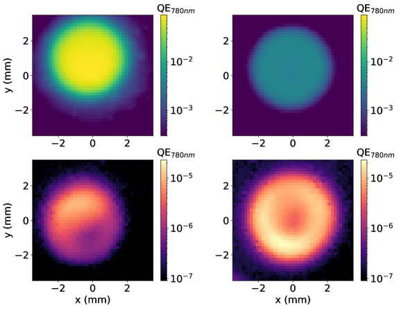
Postmortem QE maps were obtained with 780 nm light for the Cs-O activated sample #1 and Cs-Sb-O activated sample #2 in Fig. 5. The QE map demonstrates non-uniform damage on the surface, indicating that high current beam extraction caused the damage as opposed to vacuum poisoning, which we would expect to be uniform. Despite one order of magnitude lower initial QE at 780 nm, we measured a higher final QE at 780 nm for Cs-Sb-O activated sample at the damaged area () compared to that of the Cs-O activated sample (). This suggests that the Cs-Sb-O layer formed a more robust NEA layer in terms of chemical stability. Although the charge lifetime at 780 nm was not measured directly, based on the amount of charge extracted during operation () and the initial and final QE (QEi,f), we can estimate the charge lifetime at 780 nm () by assuming an exponential decay:
| (1) | |||
In Table 1, the charge lifetimes at 780 nm are estimated for the four samples. The estimated charge lifetime at 780 nm is 1.6 0.4 C for Cs-Sb-O activated GaAs and 1.1 0.1 C for Cs-O activated GaAs. Our results show that the ratio of charge lifetimes of Cs-Sb-O and Cs-O is wavelength-dependent. While it is evident from Fig. 4 that there is no improvement at 488 nm, we observe enhanced lifetimes for the former at 780 nm.
| Activation method | Initial QE at 780 nm | Final QE at 780 nm | Extracted charge (C) | Lifetime at 780 nm (C) |
| Cs-O2 #1 | ||||
| Cs-O2 #2 | ||||
| Cs-Sb-O #1 | 1.9 | |||
| Cs-Sb-O #2 | 1.3 |
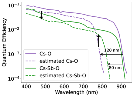
This paragraph attempts to qualitatively explain the spectral dependence of lifetime improvement based on spectral response measurements we performed in previous work.cultrera2020_LongLifetimePolarized ; bae2020_ImprovedLifetimeHigh Assuming the QE degradation is mainly due to damage done to the NEA layer, we can model the spectral response to simply shift horizontally during beam operation because of the increased work function. Based on this assumption, estimated shifts in spectral response (QE) are plotted in Fig. 6. The solid lines are the spectral response curves of Cs-O activated GaAs and Cs-Sb-O activated GaAs from our previous measurements.cultrera2020_LongLifetimePolarized ; bae2020_ImprovedLifetimeHigh The dashed lines have been obtained by simply shifting the same curves along the wavelength axis until the QE at 488 nm drops to the estimated QE after a 5 C extraction. Note 5 C is about half of what we extracted in Fig. 4. The charge lifetimes at 488 nm in Fig. 4 were used (15 C for Cs-O activated GaAs and 12 C for Cs-Sb-O activated GaAs). It is estimated that the spectral response would shift 120 nm for Cs-O activated GaAs and 80 nm for Cs-Sb-O activated GaAs. Despite a shorter lifetime at 488 nm for the Cs-Sb-O layer, the horizontal shift, or the work function increase, was smaller. This is because the log slope of spectral response () at 488 nm was steeper for Cs-Sb-O activated sample (/nm) compared to that of Cs-O activated sample (/nm). In other words, the sensitivity of the work function is the culprit for the shorter lifetime at 488 nm of the Cs-Sb-O activated sample, but the work function increase itself was smaller. Since the work function increased less due to the robust NEA layer, the final QE at 780 nm was greater than that of the standard activated GaAs.
V Conclusion
In this work, we operated Cs-O and Cs-Sb-O activated GaAs photocathodes at 200 keV with 1 mA average beam current to observe if a more chemically robust activation layer translated into an improvement in the charge lifetime under a high voltage environment. We observed a 45% improvement in charge lifetime at 780 nm for the Cs-Sb-O activated GaAs. This improvement at infrared wavelength does not correspond to an improvement at 488 nm, where instead, the lifetime was shorter. These results are interpreted in terms of work function increase induced by ion-back-bombardment. The larger lifetime at 780 nm suggests a smaller work function increase for the Cs-Sb-O case. Our results show that lifetime measurements at a single wavelength are not sufficient to fully characterize the robustness of NEA layers in operational conditions.
For future work, characterizing spectral response during the beam operation can help understand the nature of spectral dependence of lifetime improvements. The effect of thermal desorption also needs to be identified. Lastly, Cs-Sb-O activated GaAs can have a high initial QE by activating in a chamber connected to the beamline.
VI Acknowledgments
This work was supported by the Department of Energy under Grant No.DE-SC0021425 and the National Science Foundation under Grant No.PHY-1549132, the Center for Bright Beams. The authors would like to acknowledge Joe Grames for valuable discussions.
References
- [1] Lawrence S. Cardman. The PEPPo method for polarized positrons and PEPPo II. AIP Conference Proceedings, 1970(May), 2018.
- [2] C Adolphson. A large hadron electron collider at cern, physics, machine, detector. Technical report, LHeC-Note-2011-003-GEN, 2011.
- [3] Masahiko Suzuki, Michihiro Hashimoto, Tsuneo Yasue, Takanori Koshikawa, Yasuhide Nakagawa, Taro Konomi, Atsushi Mano, Naoto Yamamoto, Makoto Kuwahara, Masahiro Yamamoto, Shoji Okumi, Tsutomu Nakanishi, Xiuguang Jin, Toru Ujihara, Yoshikazu Takeda, Teruo Kohashi, Takashi Ohshima, Takashi Saka, Toshihiro Kato, and Hiromichi Horinaka. Real Time Magnetic Imaging by Spin-Polarized Low Energy Electron Microscopy with Highly Spin-Polarized and High Brightness Electron Gun. Applied Physics Express, 3(2):026601, January 2010.
- [4] M. Kuwahara, S. Kusunoki, X. G. Jin, T. Nakanishi, Y. Takeda, K. Saitoh, T. Ujihara, H. Asano, and N. Tanaka. 30-kV spin-polarized transmission electron microscope with GaAs–GaAsP strained superlattice photocathode. Applied Physics Letters, 101(3):033102, July 2012.
- [5] R. Vollmer, M. Etzkorn, P. S.Anil Kumar, H. Ibach, and J. Kirschner. Spin-polarized electron energy loss spectroscopy of high energy, large wave vector spin waves in ultrathin fcc co films on cu(001). Physical Review Letters, 91(14):1–4, 2003.
- [6] J. Grames, R. Suleiman, P. A. Adderley, J. Clark, J. Hansknecht, D. Machie, M. Poelker, and M. L. Stutzman. Charge and fluence lifetime measurements of a dc high voltage GaAs photogun at high average current. Physical Review Special Topics - Accelerators and Beams, 14(4):043501, April 2011.
- [7] Jai Kwan Bae, Luca Cultrera, Philip DiGiacomo, and Ivan Bazarov. Rugged spin-polarized electron sources based on negative electron affinity GaAs photocathode with robust Cs 2 Te coating. Applied Physics Letters, 112(15):154101, April 2018.
- [8] Jai Kwan Bae, Alice Galdi, Luca Cultrera, Frank Ikponmwen, Jared Maxson, and Ivan Bazarov. Improved lifetime of a high spin polarization superlattice photocathode. Journal of Applied Physics, 127(12):124901, March 2020.
- [9] Luca Cultrera, Alice Galdi, Jai Kwan Bae, Frank Ikponmwen, Jared Maxson, and Ivan Bazarov. Long lifetime polarized electron beam production from negative electron affinity GaAs activated with Sb-Cs-O: Trade-offs between efficiency, spin polarization, and lifetime. Physical Review Accelerators and Beams, 23(2):023401, February 2020.
- [10] Daniel Pierce and Felix Meier. Photoemission of spin-polarized electrons from GaAs. Physical Review B, 13(12), 1976.
- [11] Wei Liu, Matt Poelker, Xincun Peng, Shukui Zhang, and Marcy Stutzman. A comprehensive evaluation of factors that influence the spin polarization of electrons emitted from bulk GaAs photocathodes. Journal of Applied Physics, 122(3):035703, July 2017.
- [12] Wei Liu, Yiqiao Chen, Wentao Lu, Aaron Moy, Matthew Poelker, Marcy Stutzman, and Shukui Zhang. Record-level quantum efficiency from a high polarization strained GaAs/GaAsP superlattice photocathode with distributed Bragg reflector. Applied Physics Letters, 109(25):252104, December 2016.
- [13] Luca Cultrera, Jared Maxson, Ivan Bazarov, Sergey Belomestnykh, John Dobbins, Bruce Dunham, Siddharth Karkare, Roger Kaplan, Vaclav Kostroun, Yulin Li, Xianghong Liu, Florian Löhl, Karl Smolenski, Zhi Zhao, David Rice, Peter Quigley, Maury Tigner, Vadim Veshcherevich, Kenneth Finkelstein, Darren Dale, and Benjamin Pichler. Photocathode behavior during high current running in the Cornell energy recovery linac photoinjector. Physical Review Special Topics - Accelerators and Beams, 14(12):120101, December 2011.
- [14] Wei Liu, Shukui Zhang, Marcy Stutzman, and Matt Poelker. Effects of ion bombardment on bulk GaAs photocathodes with different surface-cleavage planes. Physical Review Accelerators and Beams, 19(10):103402, October 2016.
- [15] N Chanlek, J D Herbert, R M Jones, L B Jones, K J Middleman, and B L Militsyn. The degradation of quantum efficiency in negative electron affinity GaAs photocathodes under gas exposure. Journal of Physics D: Applied Physics, 47(5):055110, February 2014.
- [16] M. Kuriki, C. Shonaka, H. Iijima, D. Kubo, H. Okamoto, H. Higaki, K. Ito, M. Yamamoto, T. Konomi, S. Okumi, M. Kuwahara, and T. Nakanishi. Dark-lifetime degradation of GaAs photo-cathode at higher temperature. Nuclear Instruments and Methods in Physics Research Section A: Accelerators, Spectrometers, Detectors and Associated Equipment, 637(1):S87–S90, May 2011.
- [17] J T Yoskowitz, G A Krafft, G Palacios-Serrano, S Wijethunga, J Grames, J Hansknecht, C Hernandez-Garcia, M Poelker, M Stutzman, and R Suleiman. IMPROVING THE OPERATIONAL LIFETIME OF THE CEBAF PHOTO- GUN BY ANODE BIASING. Proceedings of the 12th International Particle Accelerator Conference, IPAC2021, 2021.
- [18] Jyoti Biswas, Omer Rahman, and Erdong Wang. Study of Photocathode Surface Damage due to Ion Back-Bombardment in High Current DC Gun. Proceedings of the North American Particle Accelerator Conference, NAPAC2019, 2019.
- [19] G. A. Mulhollan and J. C. Bierman. Enhanced chemical immunity for negative electron affinity GaAs photoemitters. Journal of Vacuum Science & Technology A: Vacuum, Surfaces, and Films, 26(5):1195–1197, September 2008.
- [20] Y. Sun, R. E. Kirby, T. Maruyama, G. A. Mulhollan, J. C. Bierman, and P. Pianetta. The surface activation layer of GaAs negative electron affinity photocathode activated by Cs, Li, and NF3. Applied Physics Letters, 95(17):174109, October 2009.
- [21] N. Kurichiyanil, J. Enders, Y. Fritzsche, and M. Wagner. A test system for optimizing quantum efficiency and dark lifetime of gaas photocathodes. Journal of Instrumentation, 14(08):P08025, 2019.
- [22] Masao Kuriki and Kazunari Masaki. Negative Electron affinity GaAs Cathode Activation with CsKTe Thin Film. Journal of Physics: Conference Series, 1350(1):012047, November 2019.
- [23] Jyoti Biswas, Erdong Wang, Mengjia Gaowei, Wei Liu, Omer Rahman, and Jerzy T. Sadowski. High quantum efficiency GaAs photocathodes activated with Cs, O 2 , and Te. AIP Advances, 11(2):025321, February 2021.
- [24] Omer Rahman, Jyoti Biswas, Mengjia Gaowei, Wei Liu, and Erdong Wang. New Activation Techniques for Higher Charge Lifetime from GaAs Photocathodes. Proceedings of the 10th Int. Particle Accelerator Conf., IPAC2019, 2019.
- [25] Cheng Feng, Yijun Zhang, Yunsheng Qian, Jian Liu, Jingzhi Zhang, Feng Shi, Xiaofeng Bai, and Jijun Zou. Improved quantum efficiency and stability of GaAs photocathode using favorable illumination during activation. Ultramicroscopy, 202(April):128–132, 2019.
- [26] Alice Galdi, William J. I. DeBenedetti, Jan Balajka, Luca Cultrera, Ivan V. Bazarov, Jared M. Maxson, and Melissa A. Hines. The effects of oxygen-induced phase segregation on the interfacial electronic structure and quantum efficiency of Cs 3 Sb photocathodes. The Journal of Chemical Physics, 153(14):144705, October 2020.
- [27] Bruce Dunham, John Barley, Adam Bartnik, Ivan Bazarov, Luca Cultrera, John Dobbins, Georg Hoffstaetter, Brent Johnson, Roger Kaplan, Siddharth Karkare, Vaclav Kostroun, Yulin Li, Matthias Liepe, Xianghong Liu, Florian Loehl, Jared Maxson, Peter Quigley, John Reilly, David Rice, Daniel Sabol, Eric Smith, Karl Smolenski, Maury Tigner, Vadim Vesherevich, Dwight Widger, and Zhi Zhao. Record high-average current from a high-brightness photoinjector. Applied Physics Letters, 102(3):034105, January 2013.
- [28] Leo R Dalesio, AJ Kozubal, and MR Kraimer. Epics architecture. Technical report, Los Alamos National Lab., NM (United States), 1991.
- [29] C. K. Sinclair, P. A. Adderley, B. M. Dunham, J. C. Hansknecht, P. Hartmann, M. Poelker, J. S. Price, P. M. Rutt, W. J. Schneider, and M. Steigerwald. Development of a high average current polarized electron source with long cathode operational lifetime. Physical Review Special Topics - Accelerators and Beams, 10(2):023501, February 2007.
- [30] R. R. Mammei, R. Suleiman, J. Feingold, P. A. Adderley, J. Clark, S. Covert, J. Grames, J. Hansknecht, D. Machie, M. Poelker, T. Rao, J. Smedley, J. Walsh, J. L. McCarter, and M. Ruiz-Osés. Charge lifetime measurements at high average current using a K 2 CsSb photocathode inside a dc high voltage photogun. Physical Review Special Topics - Accelerators and Beams, 16(3):033401, March 2013.