Fully Automatic In-Situ Reconfiguration of RF Photonic Filters in a CMOS-Compatible Silicon Photonic Process
Abstract
Automatic reconfiguration of optical filters is the key to novel flexible RF photonic receivers and Software Defined Radios (SDRs). Although silicon photonics (SiP) is a promising technology platform to realize such receivers, process variations and lack of in-situ tuning capability limits the adoption of SiP filters in widely-tunable RF photonic receivers. To address this issue, this work presents a first ‘in-situ’ automatic reconfiguration algorithm and demonstrates a software configurable integrated optical filter that can be reconfigured on-the-fly based on user specifications. The presented reconfiguration scheme avoids the use of expensive and bulky equipment such as Optical Vector Network Analyzer (OVNA), does not use simulation data for reconfiguration, reduces the total number of thermo-optic tuning elements required and eliminates several time consuming configuration steps as in the prior art. This makes this filter ideal in a real world scenario where user specifies the filter center frequency, bandwidth, required rejection filter type (Butterworth, Chebyshev, etc.) and the filter is automatically configured regardless of process, voltage temperature (PVT) variations. We fabricated our design in AIM Photonics’ Active SiP process and have demonstrated our reconfiguration algorithm for a second-order filter with 3dB bandwidth of 3 GHz, 2.2 dB insertion loss and 30 dB out-of-band rejection using only two reference laser wavelength settings. Since the filter photonic integrated circuit (PIC) is fabricated using a CMOS-compatible SiP foundry, the design is manufacturable with repeatable and scalable performance suited for its integration with electronics to realize complex chip-scale RF photonic systems.
Index Terms:
Silicon photonics, optical filter, automatic tuning, integrated optics, thermal crosstalk, programmable photonics, reconfigurable optics, calibration, tuning algorithm, feedback control.I Introduction
Integrated radio-frequency (RF) photonics is rapidly emerging as a technology enabler of demanding application scenarios which require capabilities beyond those of traditional electronic systems. These capabilities include ultra-wide bandwidth, exceptional low latency, long-distance routing and immunity to electromagnetic interference (EMI) [1, 2, 3, 4, 5, 6]. For any RF photonic integrated circuit (IC), optical filters are essential building blocks. The desirable feature that distinguishes RF photonic filters from their electronic, microwave and micro-electromechanical systems (MEMS) counterparts is their tunability over a very wide range of center frequencies (1 to 100s of GHz) and very wide bandwidth. Consequently, RF photonic filters offer unprecedented reconfiguration capabilities (center frequency, bandwidth, filter type, and rejection) that is inconceivable with electronic ICs alone [2, 6]. However, for their wider adoption in frequency-agile RF photonic receivers or Software Defined Radios (SDR), filter reconfiguration has to be rapid and in-situ, i.e., automatic and free from any manual intervention [7].
Traditionally, RF photonic systems have been implemented using discrete and bulky photonic components that are power inefficient, expensive and most importantly, are not amenable to integration of complex systems. Silicon Photonics, on the other hand, leverages the unique capabilities of photonic signal processing while takes full advantage of the mature CMOS-like fabrication processes developed by the semiconductor industry [8, 9, 7]. This means, an optical filter realized in a silicon photonic platform is area and power efficient, robust, scalable and can be manufactured on large-scale at a lower cost. However, due to process-induced random variations, any filter designed in a silicon photonic process will deviate from its intended characteristics. Therefore, a scheme is required that not only reconfigures the filter automatically but also is robust against process, voltage and temperature (PVT) variations.
Reconfiguration and tuning of integrated optical filters has been pursued in the literature. In ref. [10], only center frequency tuning was addressed whereas in refs. [11, 12, 13, 14], both center frequency and bandwidth were tunable. However, none of these works pursued out-of-band rejection tuning in the filter. Moreover, the filter reconfiguration was not fully automatic and heavily relied upon manual tuning. The first fully automatic tuning of silicon photonic filter was recently demonstrated in a path-breaking work by Choo et. al. in ref. [7]. However, the reconfiguration process involved the use of bulky and cost prohibitive equipment, i.e., an Optical Vector Network Analyzer (OVNA) to extract ring losses using Jones Matrix based method [7, 15].
The fundamental novelty of this work is that it achieves a truly in-situ automatic optical filter reconfiguration solution that has been experimentally demonstrated using a CMOS-compatible silicon-on-insulator (SOI) photonic process. We present an algorithm different from the one in ref. [7] which precludes the use of OVNA and eliminates several time consuming steps during the reconfiguration process. In addition, our filter also uses less number of thermal tuning elements than [7]. The designed filter has a compact form factor and is the first such filter fabricated in AIM Photonics’ Active Photonic process. Furthermore, a simplified analytical framework for the design of reconfigurable filters using analog switch-based couplers is provided and the filter PIC simulation leverages our open-source simulation code [16].
II Filter design, fabrication and Packaging
II-A Filter Topology
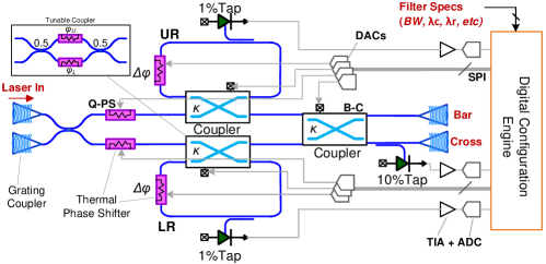
The schematic of the second-order filter topology used in this work is shown in Fig. 1. The input continuous-wave (CW) laser is fed to both arms of an outer Mach Zehnder Interferometer (MZI) through a 3dB coupler. Each arm of the MZI is loaded with a microring (UR/LR) via a tunable coupler (UR-C/LR-C) and quadrature phase-shifter (Q-PS). The two tunable couplers are in turn realized using a MZI switch as shown in the inset of Fig. 1. Another tunable coupler (Back coupler, B-C) is used at the end of the MZI to allow control over the residual imbalance in the optical field between the two arms of MZI caused by process variations. To monitor the ring resonance, a 1% tap followed by an on-chip Ge-photodetector (PD) is used in each ring. Although this directly translates to increased passband loss of the filter, these taps are an integral part of the automatic software reconfiguration algorithm [7]. Another 10% monitor tap is used at the cross port of the filter for out-of-band rejection tuning. The automatic calibration and tuning algorithm are implemented with the help of on-chip thermo-optic phase-shifters or microheaters. Both arms of the outer MZI, both the rings, and all three tunable couplers employ microheaters.
As mentioned earlier, the three tunable couplers used in the RF photonic filter are realized using analog MZI switches. The coupling matrix, , for these switches is expressed as [17]
| (1) | |||
| (2) |
Here, is the common-mode phase shift, is the differential phase shift, and and are the cross and through optical power coupling coefficients respectively. The additional phase is due to the propagation delay, , in the switch due to its physical length. Here, is the effective index. Moreover, and , are the phase shifts induced in the upper and lower arm microheaters in the switch respectively. By tuning , we obtain the power cross-coupling coefficient
| (3) | ||||
| (4) |
and the through-coupling coefficient, . The (cross-)coupling coefficient is tuned by applying microheater electrical power, , to one of the two microheaters in the switch (i.e. and ). This implies the common-mode phase shift is given by
| (5) |
Also, in Eq. 4, represents the random phase offset in the switch and is a proportionality constant relating the applied power to the thermo-optic phase-shifter.
The z-domain through (all-pass) and drop (bandpass) transfer functions of a single ring in the filter seen in Fig. 1 are derived as-
| (6) |
| (7) |
where and are the cross- and through-coupling coefficients for the 1% monitor, and is the loss factor in the ring and is the ring length. Here, , where the single-mode SOI waveguide loss is 2-2.5dB/cm [18].
A desired filter polynomial, G(z), can be synthesized using the coupled all-pass decomposition (APD) method by employing sum and difference of two all-pass filters (APF), and , as and . For even-order filters, we have [19, 20]. The -order APD filter seen in Fig. 1 had two ring APF arms and the sum or difference is realized using the back-coupler, B-C. The resulting filter output bar and cross transfer functions are
| (8) |
In our notation, and are the power coupling coefficient and phase shift in the ring, and are the back-coupler cross and through coupling coefficients, and is the quadrature phase shift.
II-B Filter Synthesis
Filter design starts with the synthesis of a polynomial, G(z), for the specified filter type and specifications. Then the denominators of the coupled all-pass polynomials, , corresponding to G(z), and constant phase were obtained using the tf2ca function in Matlab™. Then numerators were obtained using and . This yielded the two all-pass transfer functions and . Next, the all-pass transfer functions are mapped to the (cascade of) ring resonators in the upper and lower arms. If the roots of denominators , i.e. the poles of , are , then the cross-coupling coefficients are determined using and . The phase . The quadrature phase shift for the upper arm is obtained as . The lower arm coupling coefficients are identical to those of the upper arm, and and are of opposite sign, representing the conjugate APF responses. In this work, we used a -order Butterworth response with a normalized cutoff frequency of . The synthesized filter coefficients for the filter specifications are listed in Table I.
| Ring (n) | |||
|---|---|---|---|
| 1 (UR) | 0.4385 | -0.2969 | Top: -1.6137 |
| 2 (LR) | 0.4385 | 0.2969 | Bot: 1.6137 |
II-C PIC Design and Fabrication
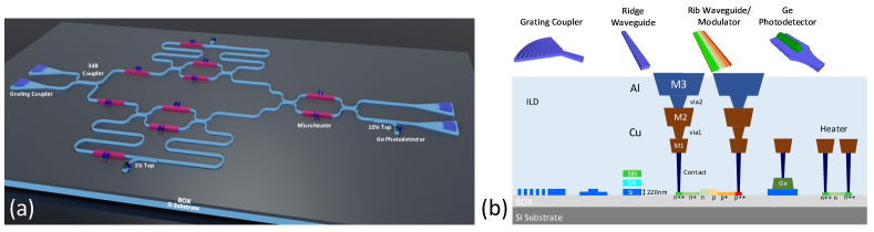
The filter was designed and fabricated in AIM Photonics foundry’s 300mm Active Photonics process [21]. This design was a part of AIM’s MPW run in June, 2019. Fig. 2 shows a 3D visualization of the filter schematic seen in Fig. 1, and the process cross-section. This process features silicon-on-insulator (SOI) rib and ridge waveguides, silicon nitride waveguides, escalators, modulator doping, Germanium (Ge) detectors, and three metal layers for routing [21, 22, 23]. The PIC layout employed several process-optimized components from the PDK library [18, 22, 23]. Grating couplers (GC) were used for vertical coupling of light into the PIC. Single-mode silicon waveguides of 480nm width and 220nm height were used for routing and interconnecting the optical components in TE polarization. The analog switches were realized using doped silicon waveguide microheater sections and 3-dB couplers [24], and with a measured thermo-optic time-constant of s. The physical lengths of the microheaters and switches are around 100 and 550, respectively.
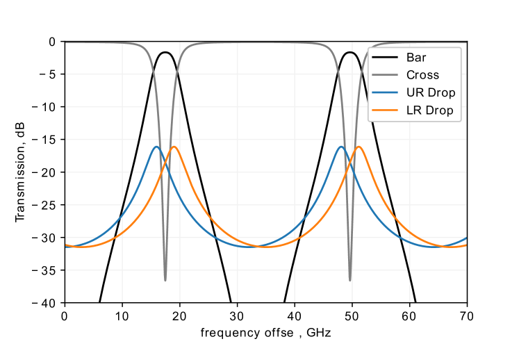
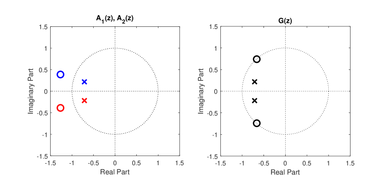
The filter was simulated using Lumerical Interconnect [25] with the AIM PDK library, as well as our open-source Python-based PIC simulator [16] built using the PhotonTorch photonic simulation framework [26]. Fig. 3(a) shows the simulated bar and cross responses of the filter after including all PIC parameters including the losses and delays. The peak of the optical monitors are aligned to the desired resonance frequency (or wavelength), corresponding to the ring phase, , for each of the rings. The simulated passband loss using the synthesized filter coefficients was 2.2 dB due to the ring losses with a 3dB bandwidth (BW) of 3 GHz and an out-of-band rejection of 30dB. The pole-zero plots for APFs, and bar and cross responses, i.e. and respectively, are shown in Fig. 3(b).
(a)
 (b)
(b)
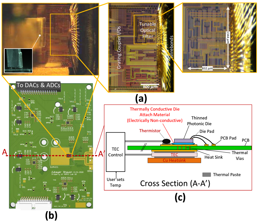
The filter layout was compacted as much as possible to share the photonic chip with other RF photonic circuits. The rings were routed in a compact serpentine fashion with a 30m bend radius for lower loss and reflections. The resulting total physical length of the rings were 2200 each, with a corresponding free-spectral range (FSR) of around 31GHz. The monitor taps were realized using 1% and 10% couplers, Ge waveguide detectors and waveguide terminations. The filter die micrograph is shown in Fig. 4(a). The filter core layout occupied 1.12 mm2 area on this chip.
II-D Packaging and Electronic Back-end
The fabricated PIC die was polished down to 150 and packaged in a chip-on-bard (COB) assembly as shown in Fig. 4(b & c). A Peltier cell and thermistor were used along with a thermo-electric cooler (TEC) controller in a closed-loop to stabilize the temperature of the chip and to minimize the thermal crosstalk among the on-chip tuning elements. The combination of die thinning and TEC at the bottom of the die provides effective thermal isolation by creating a prominent thermal gradient in the vertical direction [7].
The electrical pads were placed on two rows on the East edge of the PIC which were wire-bonded with two rows of PCB pads. The optical monitors were connected to the on-board transimpedance amplifiers (TIAs), whose outputs were interfaced with commercial off the shelf (COTS) 16-bit analog-to-digital converters (ADCs) using a ribbon cable. These pads provide 16-bit digital-to-analog converters (DACs) interfaces to the microheaters. All the DACs and ADCs communicate via SPI interface with a microcontroller, which provides a software abstraction to the algorithm code.
The operating voltage range of the microheaters is from 0 to 5V and requires a power of mW for an optical phase shift of . These voltage ranges are CMOS-compatible and the microheater driver circuits can be implemented using stacked high-voltage I/O transistors with a 5V supply voltage in 65nm CMOS (or similar) process technology [27, 28]. The TIA interface with the PDs and the 16-bit DACs and ADCs can be designed using the standard transistors in CMOS, allowing future integration of all electronics on the same chip.
III In-Situ Component Parameter Extraction
To reconfigure the SiP filter, device parameters such as the coupling ratio of the tunable couplers () and the ring phase bias () for the selected center wavelength () need to be configured. Here, stands for the ring number. These parameters are controlled by the DAC voltage (or power). Due to PVT variations in the photonic chip, there is a significant variation in the response of the tunable couplers and the phase shifters with respect to the applied power. Thus, no two couplers (or phase shifters) produce the same coupling (phase shift) for a given applied DAC voltage.
The phase shift, , produced by the microheaters linearly depends upon the applied electrical power, , as
| (9) |
However, the microheater resistance, , exhibits nonlinearity due to self-heating. Thus, applied electrical power has a nontrivial nonlinear dependence on the applied DAC voltage, . This vs characteristics must also be extracted so that we can accurately configure component parameters on the chip using the DACs. This necessitates an one-time in-situ pre-characterization of each of these components, and subsequently the configuration of them, as they are used. In this section, we provide algorithms for these pre-characterization routines and configuration.
Each of these component characterization have two steps- Part I and II. The first part, Part I, for either or extraction represents the component pre-characterization phase. On the other hand, during the automatic reconfiguration phase, this pre-characterized data is used for in-situ estimation and configuration of and parameters in the on-chip filter. Part II algorithms for both and represent these in-situ estimation and configuration.
It is important to note that Part I is a one-time operation and does not need to be repeated again as long as the filter ambient temperature is kept the same as the filter pre-characterization temperature. This is ensured by using the TEC setup seen in Fig. 4. On the other hand, Part II algorithms are invoked each time the filter is reconfigured or tuned to a different center frequency (or wavelength).
III-A Coupling Ratio () Extraction
During the initial pre-characterization routine, Algorithm 1 is executed for each of the rings in the filter. Here, to be able to configure the desired coupling ratio () of the tunable coupler of the nth ring, the wavelength response of the ring drop-port is recorded (using the monitor PDs) for a range of coupler input voltages (). From this data, the voltage () corresponding to the maximum coupling ratio () is recorded. The maximum coupling is identified by observing the quality factor (Q) of the ring drop-port resonance. Optical cavity dynamics dictate that as coupling ratio approaches unity, ring Q decreases [29]. This provides the basis for identifying the by observing the minimum Q (as shown in the bottom-right inset of Fig. 5). On the other hand, zero-coupling voltage () is identified simply by finding the corresponding to lowest monitor output at a fixed (any wavelength within one FSR in the wavelength range of interest, i.e. ). This is possible due the to very low optical power coming through the drop-port when zero-coupling is in place (as shown in the top-left inset of Fig. 5). Afterwards, the power () delivered to nth coupler microheater at different is recorded using a Keysight B2902A source measurement unit (SMU), and thus the vs characteristics are obtained. The SMU can also be realized using on-board electronics for portability [30].
Utilizing this data rather than simply relying on the quadratic relationship between voltage and power [31] ensures that the algorithm is insensitive to the electrical non-linearity of on-chip microheaters. Subsequently, the zero-coupling power () and max-coupling heater power () are obtained, and thus the power () required to obtain a phase shift in the coupler microheaters is determined as . This will subsequently serve as a reference value for the tuning algorithm to operate at different wavelengths within the FSR of the rings. It is important to note that by utilizing zero and maximum coupling rather than the critical coupling as in [7], we avoid repeated re-centering of the ring resonance at the filter center frequency () during the extraction step. Also as mentioned earlier, use of an OVNA is avoided by precluding the ring loss measurements at critical coupling for each of the rings as in the prior art in [7]. This considerably speeds up the extraction step in the filter reconfiguration algorithm (2X reduction in time) and enables in-situ tuning that can be implemented using PCB-level or chip-scale electronics.
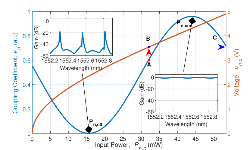
During the in-situ reconfiguration routine in Algorithm 2, first the is recorded, and depending on the , this may not be the same as the seen in Algorithm 1. Then, the raised-cosine coupling ratio vs power curve of the tunable coupler [7] from Eq. 4 and illustrated in Fig. 5 is fitted to the (, 0) & (, ) data points. From this fitted curve, power () required to set any desired coupling ratio () is estimated as shown in Fig. 5. Afterwards, from the pre-characterization vs data, the DAC voltage () needed to set a desired is determined. Here, is the maximum coupling coefficient and due to the intrinsic loss in the coupler, it never reaches unity. For our tunable coupler, it is found to be 0.959 from the foundry PDK. Furthermore, for the purpose of the filter and its usable frequency range for a free-spectral range (FSR) of 31 GHz (or 0.249 nm), the couplers can be considered broadband. Thus, all the extracted parameters are usable at any frequency (or wavelength) within the FSR.
III-B Ring Phase () Extraction
Now we describe the one-time pre-characterization routine (i.e. Algorithm 3) for the ring phase bias. First, all the rings except for the nth ring are detached from the filter by setting their corresponding couplers to zero-coupling. This ensures that the cross-port of the filter only shows the resonance response of the nth ring. Then, the voltage () required for a phase shift in the ring microheater was extracted by monitoring the cross port of the filter and shifting the resonance by full FSR (corresponding to phase-shift in the ring) for the applied voltage. Afterwards, the power () delivered to nth ring heater at different is recorded using the SMU and is obtained. As mentioned before, utilizing vs data ensures that the algorithm is insensitive to the process-dependent electrical nonlinearity of the on-chip microheaters.
During the automatic calibration routine in Algorithm 4, pre-characterized , and vs characteristics of the ring microheater is utilized. Then, from the phase-shift desired by the user, , the required microheater power change, , is estimated using Eq. 9 as
| (10) |
Meanwhile, the voltage () for which the nth ring resonance is aligned with is obtained by sweeping the ring microheater voltage () and finding the maximum drop port response. From this data, the power () at which ring resonance is aligned with is obtained. Then, the power () required to set the ring at desired is estimated as and the corresponding ring microheater voltage () is applied.
IV Automatic Tuning of Filters
The filter tuning algorithm (Algorithm 5) starts off with the user specifying the desired filter specifications. The APD filter synthesis algorithm [20, 32, 33] translates these user-defined specifications (filter type, order, bandwidth, center frequency, out-of-band suppression) to filter parameters (, & ) for all rings and MZI arms. Then the routine from Algorithm 2 is invoked and desired coupling coefficients for all ring couplers are configured by setting the microheater voltages of the ring tunable couplers to . Next, the routine from Algorithm 4 is invoked to set all the ring biases () with respect to the at their desired values. It’s important to note that due to thermal crosstalk between on-chip microheaters, every time a ring phase () is set, previously aligned rings get de-tuned and several iterations are required accurately to set all the values.
To improve the out-of-band rejection of the filter, we maximize the 10% monitor tap placed at the cross-port of the filter at by tuning the MZI quadrature-phase-shifter (Q-PS) and the back-coupler (B-C). Here, is the wavelength where a null in the filter response can be enforced.
However, the out-of-band-rejection calibration via Q-PS and B-C microheaters shifts the resonance of the previously tuned rings, thus altering the center wavelength (or frequency) of the filter response. To perform center-wavelength correction, rings, Q-PS and B-C are tuned subsequently and several iterations of tuning ( rings, Q-PS and B-C) are needed to reach the thermal steady-state of the PIC. When the required voltage stimulus is stabilized within a tolerance range (indicating a thermal steady-state), the filter tuning is complete.
It’s important to note that the coupling ratio of the tunable couplers are relatively stable in presence of thermal perturbation. This is due to the fact that thermal perturbation coming from other microheaters affect both microheaters of the tunable couplers almost equally, thus inducing a ‘common-mode’ phase shift that does not alter the coupling ratios which only depends upon the differential phase (). Therefore, it is not required to include ring coupler tuning inside the iteration loop, which in turn speeds up the reconfiguration process. Another key aspect of this algorithm is that it precludes the use of ‘outer ring’ for out-of-band rejection in [7], thus further reducing configuration time for ‘outer ring’ resonance alignment and also results in a smaller layout area.
V Experimental Results
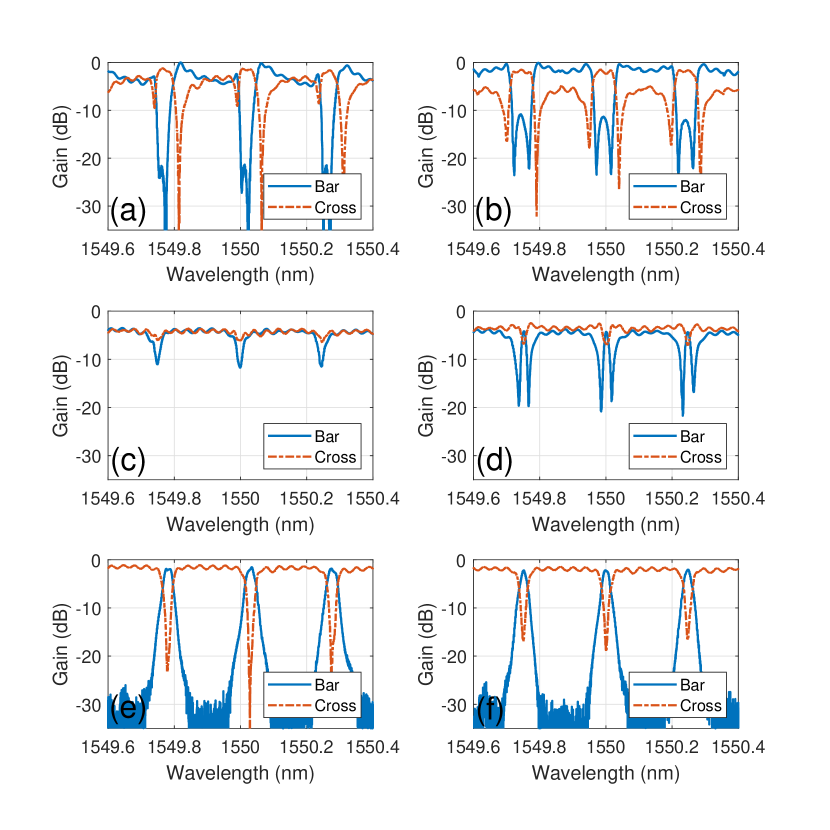
To demonstrate the functionality and efficacy of the proposed reconfiguration algorithm, the -order Butterworth filter was experimentally reconfigured using the coefficients from Table I. This filter is intended for 30dB out-of-band rejection, an insertion loss (IL) of 2.2 dB, and the 3dB bandwidth (BW) of 3 GHz at 1550nm wavelength. The 1550nm CW laser and input/outputs were coupled into the PIC using a 4-channel polarization maintaining fiber array. The fiber array was automatically aligned to the on-chip GCs.
The experimentally measured response of the filter at different stages of reconfiguration is illustrated in Fig. 6. The observed GC response exhibited 0.8dB ripple in the passband response, and the passband GC losses were de-embedded from the filter response. Unlike [7], here in this work, as soon as the Q-PS and/or B-C microheater is tuned, the previously locked UR LR rings get de-tuned due to thermal crosstalk and the center frequency of the filter shifts from its intended (in this case, = 1550 nm) as demonstrated in Fig. 6(d) and (e). Therefore, several iterations are required for automatic tuning of the filter.
Since DACs set the microheater voltages (or power), the convergence of the tuning algorithm can be observed in the settling of the DAC output voltages. In Fig. 7, the transient evolution of DAC voltages for all relevant microheaters during the tuning process is presented. Fig. 7 also shows the laser wavelength settings ( and ) that are applied to the filter input. Key events that occur during the automatic tuning process are labeled in Fig. 7 and explained in Table II. This figure shows three iterations to tune the filter (rings, Q-PS & B-C), and the time taken for the iteration progressively decreases as the filter gets closer to the thermal steady-state during tuning. In our filter layout, the Q-PS and B-C coupler were in close proximity to the rings resulting in substantial thermal crosstalk. The fabricated -order filter takes around 725 seconds to tune for the first time. The long configuration times are primarily determined by the thermal crosstalk between the components and can be significantly reduced by spreading out the layout and by employing microheaters with undercut for thermal isolation [34, 35].
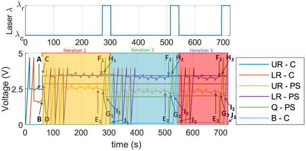
| Event | Details |
|---|---|
| Upper Ring coupler (UR-C) is set to zero coupling after a coarse and fine search. | |
| Lower Ring coupler (LR-C) is set to zero coupling after a coarse and fine search. | |
| Upper Ring coupler (UR-C) is set to desired coupling ratio based on Algorithm 2. | |
| Lower Ring coupler (LR-C) is set to desired coupling ratio based on Algorithm 2. | |
| iteration of Upper Ring phase-shifter (UR-PS) resonance alignment to after coarse and fine search. | |
| iteration of Lower Ring phase-shifter (LR-PS) resonance alignment to after coarse and fine search. | |
| iteration of configuring Upper Ring phase-shifter (UR-PS) phase bias based on Algorithm 4. | |
| iteration of configuring Lower Ring phase-shifter (LR-PS) phase bias based on Algorithm 4. | |
| iteration of maximizing 10 monitor tap output by tuning Quadrature phase-shifter (Q-PS). | |
| iteration of maximizing 10 monitor tap output by tuning Back-coupler (B-C). |
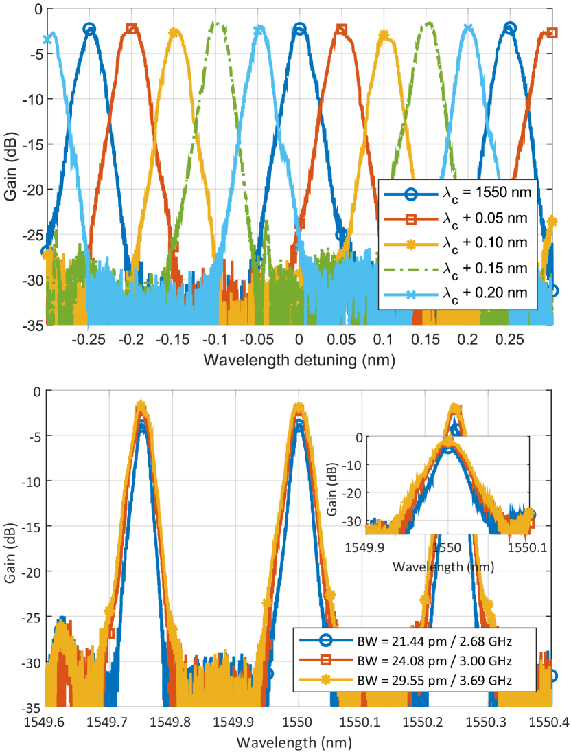
As mentioned earlier, for software defined radios (SDR) and flexible RF photonic receivers, it is vital to have filters with agile center-frequency and bandwidth tunability. To demonstrate such capability, we reconfigured the filter at 5 different center frequencies () with 0.05nm (6.25 GHz) spacing as shown in Fig. 8 (top). It’s important to note that the center frequency tuning is continuous and any center wavelength () can be configured as long as it is within the FSR of the rings. This means that the fabricated filter can be reconfigured at any frequency between DC and 31 GHz. To cover higher frequency bands, the filter can be redesigned with smaller rings (i.e. larger FSR). On the other hand, the bandwidth (BW) tunability of our proposed filter is shown in Fig. 8 (bottom) for BW = 2.68, 3 and 3.69 GHz. A trade-off can be observed in Fig. 8 (bottom), whereby as the BW is reduced, the passband insertion loss increases [13]. This becomes even more prominent when sub-GHz 3dB bandwidth settings are attempted. This is due to the losses in the rings, and can be mitigated by adopting low-loss multimode waveguide design [36] and/or utilizing the upcoming ultra low-loss PDK from AIM Photonics [21].
In Table III, a comprehensive comparison of this work with other related work such as -order APD filter [7], -order APD filter [7], -order CROW filter [10], -order CROW filter [11], -order APD filter [13], Benes switch matrix based filter [37], filter based on phase-to-intensity modulation conversion [38] and higher order vernier filter [39] is provided. As evident from the comparison, this work presents a first fully-automatic filter tuning scheme with in-situ reconfiguration capability and a significant step towards a portable solution.
| Metric |
|
|
|
|
|
|
|
|
|
|||||||||||||||||||
| Technology | AIM |
|
|
|
|
|
SiP | SiP |
|
|||||||||||||||||||
| Architecture | APD | APD | APD | CROW | CROW | APD | Benes | PM-IM | Vernier | |||||||||||||||||||
| Order | 2 | 2 | 4 | 5 | 2 | 4 | 2, 4 | - | 4 | |||||||||||||||||||
| FSR (nm) |
|
|
|
|
|
|
|
- |
|
|||||||||||||||||||
| BW (GHz) | 3 | 6.89 | 5 | 30.9 | 33.4 | 1 | 46, 56 | 1.93 | 39 | |||||||||||||||||||
| Rejection (dB) | 30 | 32 | 33 | 50 | 25 | 25 | 16, 23.4 | 18 | 50 | |||||||||||||||||||
| Passband Insertion Loss (dB) | 2.2 | 2.3 | 4.67 | 2.64 | 2.11 | 6 | 10.3, 11.2 | 38.9 | 4.5 | |||||||||||||||||||
| Reconfigurability | Y | Y | Y | Y | Y | Y | Y | Y | Y | |||||||||||||||||||
| BW | Y | Y | Y | N | Y | Y | Y | N | N | |||||||||||||||||||
| Rejection | Y | Y | Y | N | N | Y | N | N | N | |||||||||||||||||||
| Automatic Reconfiguration | Y | Y | Y | Y | Y | N | N | N | Y | |||||||||||||||||||
| BW | Y | Y | Y | N | Y | N | N | N | N | |||||||||||||||||||
| Rejection | Y | Y | Y | N | N | N | N | N | N | |||||||||||||||||||
| Portability |
|
|
|
- | - | - | - | - | - | |||||||||||||||||||
VI Conclusion and Future Work
This work presented a robust silicon photonic filter for RF photonic applications with an improved reconfiguration algorithm that is insensitive to PVT variations. By utilizing proposed in-situ configuration algorithm with simpler pre-characterization steps (i.e. without requiring an OVNA), we have experimentally shown that the filter can be configured to any desired center frequency, bandwidth and rejection as per the user specifications with high fidelity. Moreover, the filter is a first of its class to be fabricated in AIM photonics’s CMOS compatible Active Photonic process, making the filter widely manufacturable at low cost for next-generation RF photonic systems. The proposed coupling coefficient extraction and configuration algorithm provides upto 2X improvement in configuration time over the prior art.
Further improvements such as sub-GHz bandwidth with low insertion loss can potentially be achieved by incorporating multimode low-loss waveguide designs [36] and 1 monitor taps in the rings, and/or leveraging the planned ultra-low-loss PDK and MPW runs from AIM Photonics [21]. The current -order filter initial reconfiguration time is around 725s. With our optimized algorithm and a low thermal crosstalk design where back-coupler and quadrature phase shifter tuning does not affect the ring bias () as in [7], the filter reconfiguration time can be as fast as 300s. This can be achieved by careful planning of PIC layout where the thermo-optic phase-shifters (microheaters) are placed further apart from sensitive waveguides (rings) at the expense of a larger footprint. Achieving rapid filter reconfiguration on the order of seconds in frequency-agile SDRs will require even higher thermal isolation between on-chip photonic components. This can potentially be achieved by integration of microheaters with undercut [35] in the SiP foundry process. In summary, by taking full advantage of the large-volume low-cost manufacturing of a CMOS-compatible photonic process, the presented RF photonic filters and improved reconfiguration algorithm provide a way forward for wider adoption in high-performance RF and microwave photonic transceivers.
VII Acknowledgment
The authors gratefully acknowledge the generous funding support from the Air Force Office of Sponsored Research (AFOSR) YIP Award FA9550-17-1-0076 and DARPA YFA Award HR00112110001.
References
- [1] J. Capmany, G. Li, C. Lim, and J. Yao, “Microwave photonics: current challenges towards widespread application,” Optics express, vol. 21, no. 19, pp. 22 862–22 867, 2013.
- [2] V. J. Urick, K. J. Williams, and J. D. McKinney, Fundamentals of microwave photonics. John Wiley & Sons, 2015.
- [3] X. Yi, S. X. Chew, S. Song, L. Nguyen, and R. Minasian, “Integrated microwave photonics for wideband signal processing,” in Photonics, vol. 4. Multidisciplinary Digital Publishing Institute, 2017, p. 46.
- [4] R. A. Minasian, E. Chan, and X. Yi, “Microwave photonic signal processing,” Optics Express, vol. 21, no. 19, pp. 22 918–22 936, 2013.
- [5] D. Marpaung, C. Roeloffzen, R. Heideman, A. Leinse, S. Sales, and J. Capmany, “Integrated microwave photonics,” Laser & Photonics Reviews, vol. 7, no. 4, pp. 506–538, 2013.
- [6] W. Zhang and J. Yao, “Silicon-based integrated microwave photonics,” IEEE Journal of Quantum Electronics, vol. 52, no. 1, pp. 1–12, 2015.
- [7] G. Choo, S. Cai, B. Wang, C. K. Madsen, K. Entesari, and S. Palermo, “Automatic Monitor-Based Tuning of Reconfigurable Silicon Photonic APF-Based Pole/Zero Filters,” Journal of Lightwave Technology, vol. 36, no. 10, pp. 1899–1911, 2018.
- [8] R. Won, “Integrating silicon photonics,” Nature photonics, vol. 4, no. 8, pp. 498–499, 2010.
- [9] W. Bogaerts and L. Chrostowski, “Silicon photonics circuit design: methods, tools and challenges,” Laser & Photonics Reviews, vol. 12, no. 4, p. 1700237, 2018.
- [10] J. C. Mak, W. D. Sacher, T. Xue, J. C. Mikkelsen, Z. Yong, and J. K. Poon, “Automatic resonance alignment of high-order microring filters,” IEEE Journal of Quantum Electronics, vol. 51, no. 11, pp. 1–11, 2015.
- [11] J. C. Mak, A. Bois, and J. K. Poon, “Programmable multiring butterworth filters with automated resonance and coupling tuning,” IEEE Journal of Selected Topics in Quantum Electronics, vol. 22, no. 6, pp. 232–240, 2016.
- [12] B. Guan, S. S. Djordjevic, N. K. Fontaine, L. Zhou, S. Ibrahim, R. P. Scott, D. J. Geisler, Z. Ding, and S. B. Yoo, “Cmos compatible reconfigurable silicon photonic lattice filters using cascaded unit cells for rf-photonic processing,” IEEE Journal of Selected Topics in Quantum Electronics, vol. 20, no. 4, pp. 359–368, 2013.
- [13] M. S. Rasras, D. M. Gill, S. S. Patel, K.-Y. Tu, Y.-K. Chen, A. E. White, A. T. Pomerene, D. N. Carothers, M. J. Grove, D. K. Sparacin, J. Michel, M. A. Beals, and L. C. Kimerling, “Demonstration of a fourth-order pole-zero optical filter integrated using CMOS processes,” Journal of Lightwave Technology, vol. 25, no. 1, pp. 87–92, 2007.
- [14] S. Liao, Y. Ding, C. Peucheret, T. Yang, J. Dong, and X. Zhang, “Integrated programmable photonic filter on the silicon-on-insulator platform,” Optics Express, vol. 22, no. 26, pp. 31 993–31 998, 2014.
- [15] J. Kim, W. J. Sung, O. Eknoyan, and C. K. Madsen, “Linear photonic frequency discriminator on as 2 s 3-ring-on-ti: Linbo 3 hybrid platform,” Optics Express, vol. 21, no. 21, pp. 24 566–24 573, 2013.
- [16] V. Saxena, “PICTorch: Photonic Integrated Circuit Simulator,” 2022. [Online]. Available: https://github.com/AMPIC/PICTorch
- [17] J. Capmany and D. Pérez, Programmable Integrated Photonics. Oxford University Press, 2020.
- [18] “AP SUNY Component Library.” [Online]. Available: https://www.aimphotonics.com/apsuny-component-library
- [19] P. A. Regalia, S. K. Mitra, and P. Vaidyanathan, “The digital all-pass filter: A versatile signal processing building block,” Proceedings of the IEEE, vol. 76, no. 1, pp. 19–37, 1988.
- [20] C. Madsen, “Efficient architectures for exactly realizing optical filters with optimum bandpass designs,” Photonics Technology Letters, IEEE, vol. 10, no. 8, pp. 1136–1138, 1998.
- [21] “Aim photonics, url: http://www.aimphotonics.com/pdk/.” [Online]. Available: http://www.aimphotonics.com/pdk/
- [22] E. Timurdogan, Z. Su, C. V. Poulton, M. J. Byrd, S. Xin, R.-J. Shiue, B. R. Moss, E. S. Hosseini, and M. R. Watts, “Aim process design kit (aimpdkv2. 0): Silicon photonics passive and active component libraries on a 300mm wafer,” in Optical Fiber Communication Conference. Optical Society of America, 2018, pp. M3F–1.
- [23] N. M. Fahrenkopf, C. McDonough, G. L. Leake, Z. Su, E. Timurdogan, and D. D. Coolbaugh, “The aim photonics mpw: A highly accessible cutting edge technology for rapid prototyping of photonic integrated circuits,” IEEE Journal of Selected Topics in Quantum Electronics, vol. 25, no. 5, pp. 1–6, 2019.
- [24] M. R. Watts, J. Sun, C. DeRose, D. C. Trotter, R. W. Young, and G. N. Nielson, “Adiabatic thermo-optic mach–zehnder switch,” Optics letters, vol. 38, no. 5, pp. 733–735, 2013.
- [25] Ansys, “Lumerical interconnect.” [Online]. Available: https://www.lumerical.com/products/interconnect/
- [26] F. Laporte, J. Dambre, and P. Bienstman, “Highly parallel simulation and optimization of photonic circuits in time and frequency domain based on the deep-learning framework pytorch,” Scientific reports, vol. 9, no. 1, pp. 1–9, 2019.
- [27] C. Li, K. Yu, J. Rhim, K. Zhu, N. Qi, M. Fiorentino, T. Pinguet, M. Peterson, V. Saxena, and S. Palermo, “A 3d-integrated 56 gb/s nrz/pam4 reconfigurable segmented mach-zehnder modulator-based si-photonics transmitter,” in 2018 IEEE BiCMOS and Compound Semiconductor Integrated Circuits and Technology Symposium (BCICTS). IEEE, 2018, pp. 32–35.
- [28] K. Zhu, V. Saxena, X. Wu, and W. Kuang, “Design considerations for traveling-wave modulator-based cmos photonic transmitters,” IEEE Transactions on Circuits and Systems II: Express Briefs, vol. 62, no. 4, pp. 412–416, 2015.
- [29] W. Bogaerts, P. De Heyn, T. Van Vaerenbergh, K. De Vos, S. Kumar Selvaraja, T. Claes, P. Dumon, P. Bienstman, D. Van Thourhout, and R. Baets, “Silicon microring resonators,” Laser & Photonics Reviews, vol. 6, no. 1, pp. 47–73, 2012.
- [30] EasySMU: I2C Address Translator and Simple Multichannel Source Measurement Unit, Analog Devices, 2021. [Online]. Available: https://www.analog.com/en/design-center/evaluation-hardware-and-software/evaluation-boards-kits/dc2591a.html
- [31] H. Li, G. Balamurugan, M. Sakib, R. Kumar, H. Jayatilleka, H. Rong, J. Jaussi, and B. Casper, “12.1 a 3d-integrated microring-based 112gb/s pam-4 silicon-photonic transmitter with integrated nonlinear equalization and thermal control,” in 2020 IEEE International Solid-State Circuits Conference-(ISSCC). IEEE, 2020, pp. 208–210.
- [32] M. J. Shawon and V. Saxena, “Rapid simulation of photonic integrated circuits using verilog-a compact models,” in 2019 IEEE 62nd International Midwest Symposium on Circuits and Systems (MWSCAS). IEEE, 2019, pp. 424–427.
- [33] ——, “Rapid simulation of photonic integrated circuits using verilog-a compact models,” IEEE Transactions on Circuits and Systems I: Regular Papers, vol. 67, no. 10, pp. 3331–3341, 2020.
- [34] A. Masood, M. Pantouvaki, G. Lepage, P. Verheyen, J. Van Campenhout, P. Absil, D. Van Thourhout, and W. Bogaerts, “Comparison of heater architecture for thermal control of silicon photonics circuits,” in IEEE Group IV Photonics, 2013, pp. 83–84.
- [35] D. Coenen, H. Oprins, Y. Ban, F. Ferraro, M. Pantouvaki, J. Van Campenhout, and I. De Wolf, “Thermal modelling of silicon photonic ring modulator with substrate undercut,” Journal of Lightwave Technology, 2022.
- [36] D. Onural, H. Gevorgyan, B. Zhang, A. Khilo, and M. A. Popović, “Ultra-high q resonators and sub-ghz bandwidth second order filters in an soi foundry platform,” in Optical Fiber Communication Conference. Optical Society of America, 2020, pp. W1A–4.
- [37] L. Shen, L. Lu, Z. Guo, L. Zhou, and J. Chen, “Silicon optical filters reconfigured from a 16 16 benes switch matrix,” Optics Express, vol. 27, no. 12, pp. 16 945–16 957, 2019.
- [38] W. Zhang and J. Yao, “On-chip silicon photonic integrated frequency-tunable bandpass microwave photonic filter,” Optics Letters, vol. 43, no. 15, pp. 3622–3625, 2018.
- [39] H. Jayatilleka, R. Boeck, M. AlTaha, J. Flueckiger, N. A. Jaeger, S. Shekhar, and L. Chrostowski, “Automatic tuning and temperature stabilization of high-order silicon vernier microring filters,” in Optical Fiber Communication Conference. Optical Society of America, 2017, pp. Th1G–4.