Scale-dependent optimized homoepitaxy of InAs(111)A
Abstract
We combined in-situ scanning tunneling microscopy (STM) with the conventional growth characterization methods of atomic force microscopy (AFM) and reflection high energy electron diffraction (RHEED) to simultaneously assess atomic scale impurities and the larger scale surface morphology of molecular beam epitaxy (MBE) grown homoepitaxial InAs(111)A. By keeping a constant substrate temperature and indium flux while increasing the As2 flux, we find two differing MBE growth parameter regions for optimized surface roughness on the macro- and atomic scale. In particular, we show that a pure step-flow regime with strong suppression of hillock formation can be achieved, even on substrates without intentional offcut. On the other hand, an indium adatom deficient, low atomic defect surface can be observed for a high hillock density. We identify the main remaining point defect on the latter surface by comparison to STM simulations. Furthermore, we provide a method for extracting root-mean-square surface roughness values and discuss their use for surface quality optimization by comparison to scale dependent, technologically relevant surface metrics. Finally, mapping the separately optimized regions of the growth parameter space should provide a guide for future device engineering involving epitaxial InAs(111)A growth.
![[Uncaptioned image]](/html/2205.11132/assets/Figures/schematic.png)
1 Introduction
MBE growth of (001) oriented substrates is well studied in literature, while the (110) and (111)A, B orientations of InAs are examined in much less detail. The main reason being the formation of so-called hillocks, faceted surface protrusions of varying shape appearing for wide ranges of growth conditions. Formation of these is often attributed to lower arsenic sticking coefficients to the latter three crystal orientations, as stated in a recent review 1. Using few degrees off-cut substrates has repeatedly been shown to help in reducing hillocks and opening up the growth windows, however, often resulting in large atomic steps, so-called ”macrosteps”.1
Recently, the interest for (111) oriented substrates has increased due to a manifold of benefits over the (001) standard. (111)-oriented III-V compound semiconductors were proposed as growth templates for high quality V2-VI3 topological insulators due to a smaller lattice mismatch 2. InAs(111) in particular, has been under investigation as a material for novel n-channel metal-oxide-semiconductor field-effect transistors (nMOSFETs), where access to the L-valley conduction is believed to improve the technology 3. Furthermore, epitaxial heterostructures of narrow-gap IV-VI and III-V semiconductors are a promising candidate for mid-infrared photonics, where the main benefits are the lattice constant matching, mechanical strength, chemical stability, and thermal conductivity as compared to the currently used substrates 4. InAs is also the compound semiconductor of choice for building a hybrid semiconductor-superconductor based topological quantum bit, due to its unique combination of electronic properties such as e.g. large spin-orbit interaction and a narrow direct bandgap 5. InAs(111) forms a low strain interface with GaSb and AlSb, other technologically relevant III-V compound semiconductors, as well as several II-VI compound semiconductors. Hence, a better understanding of the growth of InAs(111)A would open up a range of new device architectures. Herein, we focus on A-polar samples as hillock formation has been demonstrated to be suppressed compared to B-polar substrates. The wider triangular hillocks found on the B side generally lead to poorer optical and electrical properties.1
The resurfaced interest for InAs(111)A has led to efforts of systematically mapping the MBE growth parameter space by Vallejo and coworkers in 2019 6. Optimized MBE growth conditions are reported operating with As4 species, based on reduction of root mean square (RMS) line roughness (Rq) values, extracted from large-scale (11 and 55 ) ambient AFM topographies and an increase in integrated photoluminescence intensities. With the constant miniaturization of devices, however, the atomic scale morphology and atomic impurities are becoming more important and reports on these are still rare. Commonly employed growth characterization tools such as ambient AFM, lack atomic resolution. Electron-based methods such as reflective high-energy electron diffraction (RHEED) or transmission electron microscopy (TEM) average over too large areas or volumes to yield a representative image of atomic impurities. STM on III-V materials on the other hand, provides the atomic resolution and additionally yields elemental contrast 7, allows detection of charge impurities 8 and probes the electronic properties with atomic lateral precision 9, 10. By employing an MBE with an in-situ STM, alongside conventional characterization methods we examine the MBE growth parameter space for the InAs(111)A MBE homoepitaxy to find areas of optimized surface quality on the atomic- and large-scale.
A series of samples with increasing As2 flux, based around the previously found optimal conditions for As4-based homoepitaxy 6 reveals two scale-dependent regimes, by optimization of carefully extracted root-mean-square surface roughness (Sq) values. One regime on the small scale, as probed by STM, at an As2/In flux ratio of 15 where the atomic scale surface only contains a single type of vacancy impurity alongside native charge impurities. We identified this impurity as an additional In-vacancy by comparison to density functional theory (DFT) based STM simulations and extract an approximate density of these of cm-2. Another regime on the large scale we expose an optimized pure step-flow regime at an As2/In flux ratio of 26 by AFM imaging. Furthermore, we provide a method for employing the root-mean-square surface roughness Sq as a metric for surface quality on both scales and qualify it by comparison to technologically relevant metrics. Finally, we map these results to the growth parameter space to outline areas of interest for future investigations.
2 Experimental
2.1 Molecular Beam Epitaxy
Samples were grown and analyzed in an ultra-high vacuum (UHV) cluster tool, details of which can be found in the Supplemental Material 11. A series of six InAs(111)A samples was grown by homoepitaxial MBE. Four samples with increasing As2/In flux ratio (3,15,26 and 33), keeping the indium flux constant at a corresponding growth rate of 0.07 ML/s and at a substrate temperature of TC (Samples 1-4) and two at fixed As2/In flux ratio with C offset from the initial sample temperature (Samples 5, 6). Each sample consisted of a 1010 mm2 cleaved piece of single-side polished InAs(111)A wafers (Wafer Technology Ltd., n-doped, miscut). The pieces were gallium-glued to sample plates. After an initial ten hour degas in the main tunnel loadlock at 200∘C the samples were further degassed in a dedicated heater station at 250∘C for one hour. The surface oxide was removed by ten minutes of atomic hydrogen cleaning 12 at the same temperature and with a hydrogen background pressure of mbar. This procedure resulted in sharp RHEED patterns of the only stable 22 surface reconstruction even before any buffer growth 13. Samples were kept at elevated temperatures (200∘C) until the background pressure had recovered to mbar and were then transferred to the MBE chamber.
Effective As2 fluxes for As2/In flux ratio calculations were calibrated using the GaAs(001)-(2×4)/(4×2) RHEED transition at a pyrometer sample temperature of 600∘C. Effective indium fluxes were calibrated by RHEED oscillations on InAs(001). Growth rates herein are given in monolayers (ML) of InAs(001) per second. The substrate temperature was ramped up with fully open arsenic-valve and measured using a pyrometer. The nominal thickness of the grown InAs(111)A buffer was 50 nm, with the exception of sample 2 which has a nominal thickness of 120 nm. The low indium determined growth rate of 0.07 ML/s was necessary to achieve the high As2/In flux ratio and was kept constant for all experiments to avert rate-dependent effects.
To observe the growth mode transition from islands growth to a step flow regime, RHEED intensity oscillations were recorded on a quarter of a similar 2-inch wafer for increasing arsenic flux. Due to suppressed island nucleation in a pure step-flow regime the vanishing of RHEED oscillations with increasing arsenic flux indicates the mentioned growth mode transition 14. The transition onset value of the As2/In flux ratio was estimated by linear extrapolation of the maximum oscillation amplitude with increasing flux ratio to zero. The details of which are included in the Supplemental Material 11.
It is generally known that the final ramp down can have an influence on the atomic scale cleanliness. Therefore, the procedure to ramp down the sample temperature after growth used in this study is inspired by the ramp for GaAs(001) homoepitaxy by LaBella et al. where the goal was to achieve a well-ordered surface for STM. 15 The basic principle is to ramp the sample temperature as well as As-background down as soon as the growth is done. A similar procedure was shown to preserve the adatoms densities at growth conditions 16. We chose to keep the As background pressure at growth conditions value and ramp the temperature from the value during growth to 350∘C at a rate of 2∘C/s. At this point the As valve and shutter were closed, immediately followed by ramping the substrate temperature to 250∘C at the same rate.
2.2 Scanning Probe Microscopy
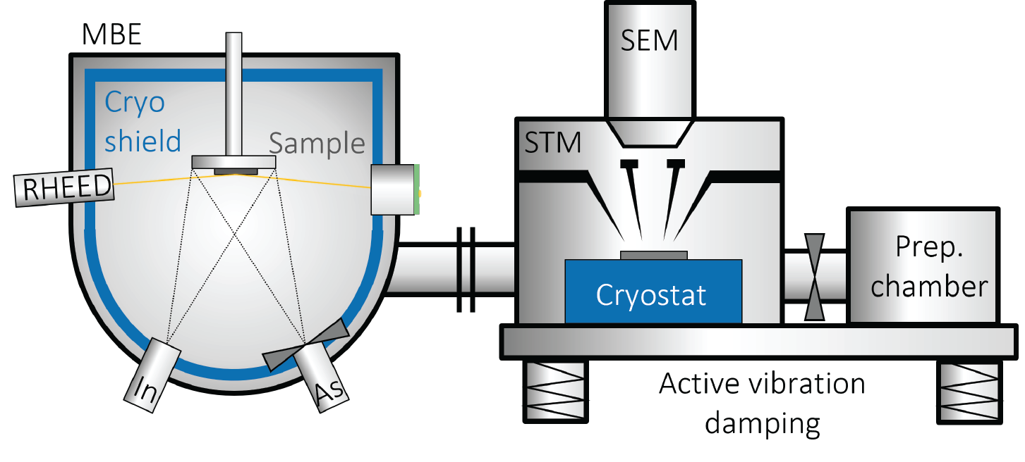
STM topographic images were recorded at liquid helium or nitrogen temperatures (4.3K or 78K), employing commercially available, electrochemically etched tungsten tips. Typical scan parameters for the topographic images consisted of a tip bias of V0.5-2.0V and tunnel current set-point of I 70-100 pA for typical scan sizes of m2 to nm2. The details of the STM (Scienta Omicron LT Nanoprobe 4P) can be found in the Supplemental Material 11. Impurity densities were extracted using the thresholding particle analysis tool in the MountainsSPIP™ software produced by Image Metrology A/S.
An AFM (Dimension Icon, Bruker), operating in ambient conditions and using Bruker’s exclusive PeakForce quantitative nanoscale mechanical characterization (QNM) mode was used to characterize the topography of samples after they were removed from the STM. Representative large scale overviews of the sample surface were acquired. Scan sizes of maximal 1010m were taken on one to three locations (see Table in Supplemental Material 11) spread evenly over the sample surface or at representative locations as determined manually by optical microscopy. Terrace widths () were extracted by manually measuring line the width of 10 consecutive terraces perpendicular to the step edges for at least 10 different local areas using MountainsSPIP™.
2.3 Computational Methods
Density functional theory (DFT) calculations were performed using the Vienna Ab-Initio Simulation Package (VASP) code 17, 18, 19, 20, 21 with the projector-augmented wave (PAW) method.22, 23 To describe the exchange-correlation interactions between electrons, the generalized gradient approximation (GGA) of Perdew, Burke, and Ernzerhof (PBE) 24 was used with a Hubbard U correction within Dudarev’s formalism 25 applied to the p-orbitals of both In and As. values were determined using a Bayesian optimization method 26, and were found to be -0.5 eV and -7.5 eV for In and As, respectively. These values have been used successfully for various simulations of InAs surfaces and interfaces.27, 26, 28 Spin orbit coupling was applied throughout 29 and a dipole correction was applied along the z-axis of the surface.30 For all self consistent field (SCF) and density of states (DOS) calculations, -centered Monkhorst-Pack k-point grids with densities of 551, and a cutoff energy of 350 eV were used.
STM simulations were performed using the Tersoff and Hamann approximation, which states that the tunneling current is proportional to the local density of states (LDOS).31 To generate the pristine 22 surface reconstruction, an In-terminated InAs(111) surface was constructed with 40Å of vacuum, using an InAs lattice parameter of 6.0584Å. Pseudo-hydrogen atoms with charges of 0.75 e- were appended to the bottom surface to passivate the dangling bonds that result from cleaving of the surface 32, and a single In atom was then removed from the top surface. Next, ionic relaxation of the top four atomic layers and the pseudo-hydrogen positions was performed until the Hellman-Feynman forces acting on ions were below 0.001 eV/Å. During relaxation the As atoms in the second atomic layer moved to 0.09Å below the top In atoms, putting them on approximately the same plane, correctly reproducing the expected surface reconstruction.33 After the relaxation finished, it was found that As dimers formed near the site of the defect. To model the In-vacancy, the relaxed InAs(111)A-(22) surface was used as a starting point and an additional In atom was removed from the center of a 44 surface unit cell. For the InAs(111)A-(22) surface model and the In-vacancy surface 16 and 10 atomic layers were used, respectively.
3 Results and Discussions
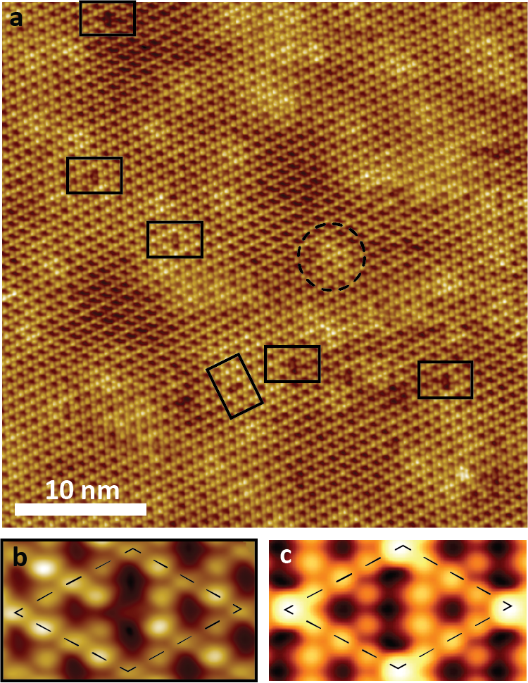
The combination of an MBE with in-situ transfer to an STM has enabled us to identify a set of MBE growth parameters for the InAs(111)A homoepitaxy, resulting in negligible amounts of indium adatoms and a low density of point defects as displayed in Figure 1. Comparing the STM topographic image to DFT based simulated STM images we were able to identify the remaining impurity. Figure 1a shows a representative atomically resolved STM topographic image of the InAs(111)A surface where black rectangles mark the positions of the singular type of observed surface impurity. Additionally, local variations in the brightness (example marked with a dashed circle in Figure 1a) hint at charge accumulation areas 8, most likely caused by indium antisites native to the InAs(111)A homoepitaxial growth 34. In Figure 1b a close-up of the marked prevailing defect in the InAs(111)A-(22) In-vacancy reconstruction is shown and the 44 surface unit cell of this defect is marked with a black dashed rhombus. The comparison to a simulated STM image of an extra indium-vacancy impurity in the InAs(111)A-(22) reconstruction in Figure 1c shows a good agreement. We can, therefore, add this extra indium vacancy to the list of stable impurities of the MBE grown InAs(111)A surface, along with the indium and As2 adsorbates 35 and the previously mentioned indium antisites. Within the limited field-of-view of STM imaging, we calculated the density of these remaining impurities to be on the order of cm-2 by manually counting them in multiple selected areas of 4040 nm2, spread over the sample. For comparison, in a recent publication by Chung and coworkers 36 an impurity density in GaAs of was considered a low-density regime where defects are purely due to MBE source impurities. Post STM, ex situ AFM revealed that the larger scale topography of the atomically clean surface contains a large amount of hillocks. This could be the reason for the vanishing of native indium adatoms by preferential incorporation into the hillock sites of remaining indium adatoms during the ramp-down of sample temperature.
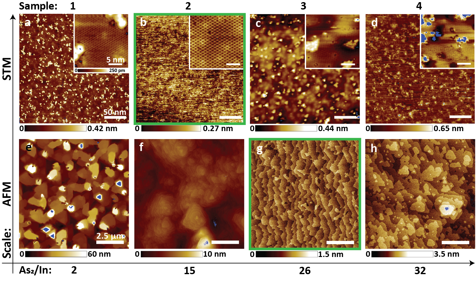
To identify the optimal growth conditions for both atomically and large scale smooth surfaces the surfaces with increasing arsenic flux were probed first with in-situ STM followed by ex-situ AFM. For an overview of the respective imaging conditions and growth details, consult the table in the Supplemental Material 11. The As2 flux was set to result in As2/In flux ratios of approximately 2, 15, 26 and 32 while keeping the In flux and the substrate temperature roughly constant (samples 1-4). Representative STM and AFM images of each sample are show in in Figure 2. The top row (Fig. 2a-d) contains 250250 nm2 STM topographic images and the insets show 2020 nm2 zoom-ins with atomic resolution. Surface impurities change in amount and type with increasing As2 flux (from left to right). In sample 1, adatom clusters and holes prevail while sample 2 is the optimised surface, as discussed previously in Figure 1. Sample 3 contains both In- and As-adatoms and many small often triangular shaped islands. Finally, sample 4 contains In-adatoms and amorphous clusters of particles of unknown origin, most probably indium adatom clusters. The small scale impurities of sample 1 and 4 are comparable in type and amount. We notice that the different appearance of the surface reconstruction in the atomically resolved insets (hexagons in Figure 2a, c and the ”true” 22 in Figure 2b) is attributed to slight changes in STM tip shape and imaging quality which depends also partly on the surface quality.
Focusing on the classic AFM growth analysis in the bottom row of Figure 2, we found a different set of optimal growth parameters, marked by a green frame, at which the amount of hillocks is greatly reduced. The representative AFM topographies shown have a size of 1010m2.
A steady increase in terrace width from few tenths of nanometer to more than half a micrometer with increasing As2 flux was extracted from manual measurements on zoomed-in versions and are visualized in the plot in Figure 3d. The terrace width at optimized step flow conditions (Fig. 2g) was found to be 500 nm. If we compare this to the average width of a terrace on the vicinal surface of an epi-ready InAs(111)A wafer the assumption that we grew in pure step flow is reasonable. Assuming formation of steps of one monolayer (ML) height with nm, following simple trigonometry, the typical miscut uncertainty of the used wafers will result at maximum in an average terrace width of nm. Therefore, the miscut of the wafer of the sample grown in step-flow mode with 500 nm wide terraces (Fig. 2a) would correspond to a miscut of , well within the margin of error. Regarding the formation of hillocks we observe an initial increase of hillock density with a peak at sample 2, followed by a reduced hillock density to levels on the order of initial larger scale defects on the bare wafer. This can also be observed easily by optical microscopy. Optical microscope images of both the bare wafer and samples 1-3 can be found in the Supplemental Material 11. It is noteworthy that this finding implies that by reducing the initial surface defects with e.g. a superlattice structure the appearance of hillocks in this regime might be able to be fully suppressed.
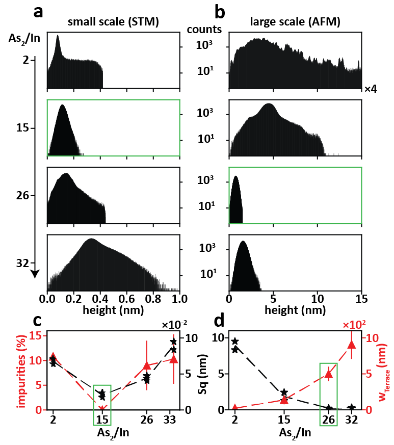
The distribution of heights in least-square (LS) plane leveled surfaces is a good indicator for the surface quality. A narrow, normal-distributed heights histogram corresponds to a smooth surface. Histograms of the STM and AFM topographies in Figures 2a-d and e-h, respectively are shown in Figure 3a, b with the ordinates in a logarithmic scale to enhance the contributions from impurities (shoulders). The two optimized surfaces, marked by green boxes, show the narrowest distributions and lack significant shoulders when fitted by a normal distribution (not shown). To convert this visually encoded information into a single metric the surface roughness can be calculated.
We now focus on the extraction method for the surface roughness and its use as a metric for surface quality. Previous reports by Vallejo et al. relied on the metric of averaged root-mean-square (RMS) line roughness (Rq) as an indicator for high surface quality. We argue here, that RMS surface roughness (Sq) is less prone to being influenced by uni-directional defects such as the step edges at the atomic scale we are interested to quantify. The question remains, whether a carefully extracted Sq value can be used as a single metric to determine both atomic scale and larger scale surface quality as compared to the technologically relevant parameters of impurity density and terrace width, respectively. Sq would have the benefit of being easily deducible compared to the latter parameters. Therefore, in Figure 3c (d) we plot the extracted Sq values from the STM (AFM) topographies in Figure 2a-d (e-h) alongside the impurity density (extracted terrace width).
The small scale Sq values in Figure 3c show a clear correlation with the surface density of impurities. For the large scale Sq values, we observe an anti-correlated behavior i.e. the surface roughness Sq decreases with increasing terrace width.
We ensured the relevance of the Sq values by excluding step edges. In case there is no terrace wide enough, masking of the other terraces was applied. Still, a direct inference of adatoms densities from the roughness values is not feasible due to multiple factors. Firstly, the quantity and quality of impurities has to be inferred from a topographic image and can not be captured in a single metric. And secondly, STM topographies always comprise a mix of topographic and electronic information. On the one hand this opens up a multitude of possibilities, on the other hand it makes it hard to deconvolute the two components. A solution can be to apply a high bias voltage, where electronic influences of the electronic structure on the topography are reduced.
The employed method to ensure the accuracy and relevance of the large scale Sq values consisted of a simple LS plane leveling. For very rough surfaces with many hillocks and wedding cake formation the observed anti-correlation may break down. In general, only the sum of multiple topographic images at different magnification will truly capture all the details of the surface quality in its complexity but the Sq values as extracted herein can aid as a fast, single-metric feedback for surface optimization.
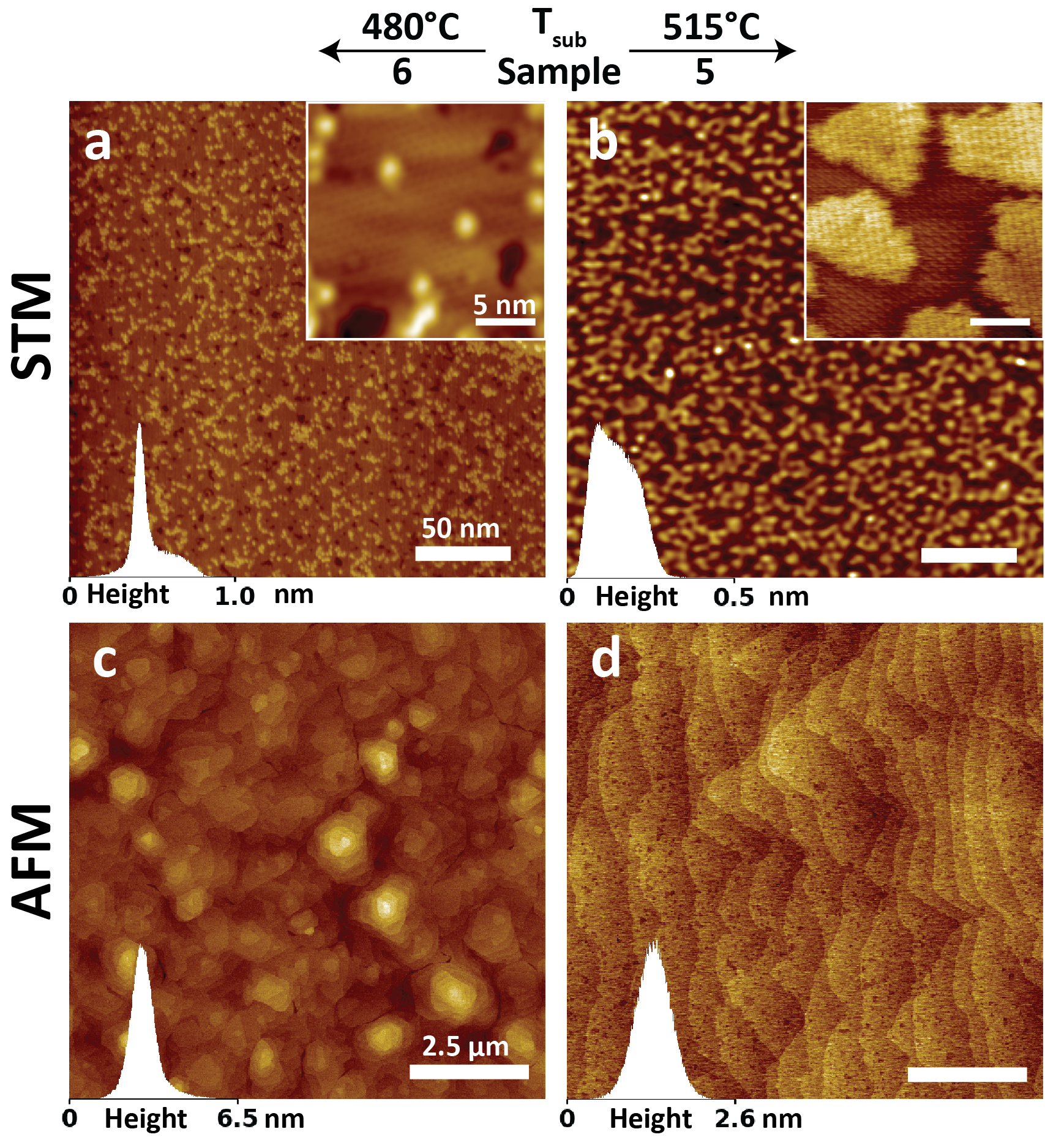
Next, we investigate the temperature range around the previously found optimal substrate temperature of 500∘C to explore the extend of the discovered step-flow region horizontally in the growth parameter space. Figures 4a, b (c, d) contain the STM (AFM) investigation at an increased and decreased substrate temperature, respectively for approximately constant As2/In flux ratio values. Generally, we observe surfaces decrease in quality for these significant deviations of the optimal growth temperature of TC. On the atomic scale (Fig. 4a, b), an increase in surface impurities for deviations in either direction from the optimal growth temperature are noted. At a lower temperature (Fig. 4a) a mix of few nanometre small holes and clusters of adatoms are observed, similar to growth results over large ranges of growth parameters outside the optimal region, compare e.g. Ref. 6. At an increased TC (Fig. 4b) the formation of a dense array of InAs islands of equivalent diameter of 5-10 nm are recorded. No such structures have been reported before and their appearance can likely be attributed to highly increased chances of decomposition of the In-As bonds above a temperature of . Such conditions, in combination with the low growth rates employed, would then lead to an effective negative flux of indium atoms and the formation and growth of a network of vacancies which could appear like islands. It may then be argued whether any growth is effectively achieved.
At a reduced TC, AFM reveals that the step-flow regime is exited and formation of wedding cake structures commences (Fig. 4c), indicating the lower boundary for step-flow in Tsub must be between 480-500∘C. The AFM topography at elevated TC (Fig. 4d) still exhibits a step-flow like surface structure with unidirectional steps of reduced terrace width and smoother step edges as compared to TC.
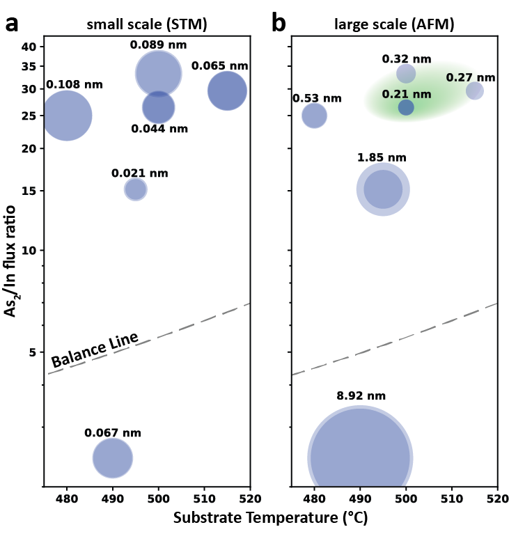
Finally, we map the extracted surface roughness values for all growths to a MBE growth parameter space to define regions of interest for future studies. This is shown in Figure 5a,b for the small and large scale Sq values, respectively. The size of the circles corresponds to the surface roughness values and multiple circles (darker blue)) indicate multiple extracted values. The areas of smallest roughness (smallest circle diameter) have clearly different centers, depending on the scale one focuses on. RHEED studies by Nomura and coworkers who experimentally found the transition from arsenic flux limited growth to indium flux limited growth (often called detailed balance line) on InAs(111)A for MBE with As2 species 37 are added to indicate the regions of indium and arsenic flux dependent growth rate regions. To validate the position of the detailed balance line for our setup we repeated similar RHEED measurements which can be found in the Supplemental Material 11. A good agreement between the balance line position we extracted and the Nomura et al. data was found. Furthermore, the region where step-flow growth was observed is marked with a green shaded area in Figure 5b. The sharper transition at a As2/In flux ratio of about 25 is argued for by the vanishing of RHEED oscillations at this value (results see Supplemental Material 11), further indicating the onset of the step-flow region. It is, therefore, believed that no single set of growth parameters exists where the two optimized regions overlap.
4 Conclusions
In conclusion, we have demonstrated the special capabilities of an in-situ MBE-SPM combination as a feedback loop for atomic scale engineering of surfaces. We showed that at different scales surface optimization results in differing MBE growth parameters, implying the need for more atomic scale analysis during growth optimization for (111) substrate based nanoscale devices. The two regions of optimized large- and small-scale surfaces are achieved at substrate growth temperatures of 500∘C and 495∘C and As2/In flux rations of 26 and 15. The former exhibits a pure step flow regime with unidirectional terraces of 500 nm and the latter up to 250 nm wide terraces with no indium adatoms and an extra indium vacancy as single prevailing surface impurity. We demonstrate the correlation of RMS surface roughness (Sq) values extracted in a careful manner with the technologically relevant metrics of terrace width and impurity density. The growth temperature space around the step flow yielding growth parameters was also probed and a dependence on the substrate temperature was observed with the surface structure changing noticeably for deviations of C. Finally, maps indicating the respective optimized regions in the MBE growth parameter space are provided as a base for focused engineering of a surface tailored to a specific application.
5 Contributions
S.Z. prepared the samples, recorded most of the STM and all AFM topographies, analyzed the data and wrote the paper. R.B. contributed to study design, recorded some of the STM topographies and contributed to editing the paper. D.D. and N.M. contributed the DFT calculations and the editing of the related parts of the text. K.G.-R. and P.K. contributed to formulating the research question and editing of the paper.
S.Z. acknowledges support from Microsoft Research, Microsoft Quantum initiative, Collaborative Project Description. Work at CMU was funded by the National Science Foundation (NSF) through grant OISE-1743717. The computer simulations used resources of the National Energy Research Scientific Computing Center (NERSC), a U.S. Department of Energy Office of Science User Facility operated under Contract No. DE-AC02-05CH11231.
References
- Yerino et al. 2017 Yerino, C. D.; Liang, B.; Huffaker, D. L.; Simmonds, P. J.; Lee, M. L. Review Article: Molecular beam epitaxy of lattice-matched InAlAs and InGaAs layers on InP (111)A, (111)B, and (110). Journal of Vacuum Science & Technology B 2017, 35, 010801
- Zeng et al. 2013 Zeng, Z.; Morgan, T. A.; Fan, D.; Li, C.; Hirono, Y.; Hu, X.; Zhao, Y.; Lee, J. S.; Wang, J.; Wang, Z. M.; Yu, S.; Hawkridge, M. E.; Benamara, M.; Salamo, G. J. Molecular beam epitaxial growth of Bi2Te3 and Sb2Te3 topological insulators on GaAs(111) substrates: a potential route to fabricate topological insulator p-n junction. AIP Advances 2013, 3, 072112
- Sumita et al. 2021 Sumita, K.; Toprasertpong, K.; Takenaka, M.; Takagi, S. Proposal and Experimental Demonstration of Ultrathin-Body (111) InAs-On-Insulator nMOSFETs With L Valley Conduction. IEEE Transactions on Electron Devices 2021, 68, 2003–2009
- Haidet et al. 2021 Haidet, B. B.; Nordin, L.; Muhowski, A. J.; Vallejo, K. D.; Hughes, E. T.; Meyer, J.; Simmonds, P. J.; Wasserman, D.; Mukherjee, K. Interface structure and luminescence properties of epitaxial PbSe films on InAs(111)A. Journal of Vacuum Science & Technology A 2021, 39, 023404
- Thomas et al. 2018 Thomas, C.; Hatke, A. T.; Tuaz, A.; Kallaher, R.; Wu, T.; Wang, T.; Diaz, R. E.; Gardner, G. C.; Capano, M. A.; Manfra, M. J. High-mobility InAs 2DEGs on GaSb substrates: A platform for mesoscopic quantum transport. Physical Review Materials 2018, 2, 1–8
- Vallejo et al. 2019 Vallejo, K. D.; Garrett, T. A.; Sautter, K. E.; Saythavy, K.; Liang, B.; Simmonds, P. J. InAs(111)A homoepitaxy with molecular beam epitaxy. Journal of Vacuum Science & Technology B 2019, 37, 061810
- Timm et al. 2009 Timm, R.; Feenstra, R. M.; Eisele, H.; Lenz, A.; Ivanova, L.; Lenz, E.; Dähne, M. Contrast mechanisms in cross-sectional scanning tunneling microscopy of GaSb/GaAs type-II nanostructures. Journal of Applied Physics 2009, 105, 093718
- Ebert 2003 Ebert, H. P. Imaging defects and dopants. Materials Today 2003, 6, 36–43
- Suzuki et al. 2019 Suzuki, K.; Onomitsu, K.; Kanisawa, K. Tunneling spectroscopy of an indium adatom precisely manipulated on the cross-sectional surface of InAs/GaSb quantum structures. Physical Review B 2019, 100
- Batabyal et al. 2022 Batabyal, R.; Zelzer, S.; Dardzinski, D.; Romagosa, A. P.; Krogstrup, P. unpublished
- 11 See Supplemental Material at supp.com for an overview table of the samples respective growth and measurement parameters, a detailed description of the MBE and STM systems used and additional optical microscope and RHEED data.
- Khatiri et al. 2004 Khatiri, A.; Ripalda, J. M.; Krzyzewski, T. J.; Bell, G. R.; McConville, C. F.; Jones, T. S. Atomic hydrogen cleaning of GaAs(0 0 1): A scanning tunnelling microscopy study. Surface Science 2004, 548, 0–5
- Veal and McConville 2000 Veal, T. D.; McConville, C. F. Controlled oxide removal for the preparation of damage-free InAs(110) surfaces. Applied Physics Letters 2000, 77, 1665–1667
- Neave et al. 1985 Neave, J. H.; Dobson, P. J.; Joyce, B. A.; Zhang, J. Reflection high-energy electron diffraction oscillations from vicinal surfaces - A new approach to surface diffusion measurements. Applied Physics Letters 1985, 47, 100–102
- La Bella et al. 1999 La Bella, V. P.; Yang, H.; Bullock, D. W.; Thibado, P. M.; Kratzer, P.; Scheffler, M. Atomic structure of the GaAs(001)-(2x4) surface resolved using scanning tunneling microscopy and first-principles theory. Physical Review Letters 1999, 83, 2989–2992
- Kanisawa 2013 Kanisawa, K. Correlation between adatom dynamics and electron accumulation at the epitaxial InAs(111)A surface. Journal of Crystal Growth 2013, 378, 8–12
- Joubert 1999 Joubert, D. From ultrasoft pseudopotentials to the projector augmented-wave method. Physical Review B 1999, 59, 1758–1775
- Kresse and Furthmüller 1996 Kresse, G.; Furthmüller, J. Efficient iterative schemes for ab initio total-energy calculations using a plane-wave basis set. Physical Review B 1996, 54, 11169–11186
- Kresse and Furthmüller 1996 Kresse, G.; Furthmüller, J. Efficiency of ab-initio total energy calculations for metals and semiconductors using a plane-wave basis set. Computational Materials Science 1996, 6, 15–50
- Kresse and Hafner 1993 Kresse, G.; Hafner, J. Ab initio molecular dynamics for open-shell transition metals. Physical Review B 1993, 48, 13115–13118
- Kresse and Hafner 1994 Kresse, G.; Hafner, J. Ab initio molecular-dynamics simulation of the liquid-metalamorphous- semiconductor transition in germanium. Physical Review B 1994, 49, 14251–14269
- Blöchl 1994 Blöchl, P. E. Projector augmented-wave method. Physical Review B 1994, 50, 17953
- Kresse and Joubert 1999 Kresse, G.; Joubert, D. From ultrasoft pseudopotentials to the projector augmented-wave method. Physical Review B 1999, 59, 1758–1775
- Perdew et al. 1996 Perdew, J. P.; Burke, K.; Ernzerhof, M. Generalized gradient approximation made simple. Physical Review Letters 1996, 77, 3865
- Dudarev et al. 1998 Dudarev, S. L.; Botton, G. A.; Savrasov, S. Y.; Humphreys, C. J.; Sutton, A. P. Electron-energy-loss spectra and the structural stability of nickel oxide: An LSDA+U study. Physical Review B 1998, 57, 1505–1509
- Yu et al. 2020 Yu, M.; Yang, S.; Wu, C.; Marom, N. Machine learning the Hubbard U parameter in DFT+U using Bayesian optimization. npj Computational Materials 2020, 6, 180
- Yang et al. 2021 Yang, S.; Dardzinski, D.; Hwang, A.; Pikulin, D. I.; Winkler, G. W.; Marom, N. First-principles feasibility assessment of a topological insulator at the InAs/GaSb interface. Physical Review Materials 2021, 5, 084204
- Yu et al. 2021 Yu, M.; Moayedpour, S.; Yang, S.; Dardzinski, D.; Wu, C.; Pribiag, V. S.; Marom, N. Dependence of the electronic structure of the EuS/InAs interface on the bonding configuration. Physical Review Materials 2021, 5, 064606
- Steiner et al. 2016 Steiner, S.; Khmelevskyi, S.; Marsmann, M.; Kresse, G. Calculation of the magnetic anisotropy with projected-augmented-wave methodology and the case study of disordered alloys. Physical Review B 2016, 93, 224425
- Neugebauer and Scheffler 1992 Neugebauer, J.; Scheffler, M. Adsorbate-substrate and adsorbate-adsorbate interactions of Na and K adlayers on Al (111). Physical Review B 1992, 46, 16067
- Tersoff and Hamann 1985 Tersoff, J.; Hamann, D. R. Theory of the Scanning Tunneling Microscope. Phys. Rev. B 1985, 31, 805–813
- Dardzinski et al. 2022 Dardzinski, D.; Yu, M.; Moayedpour, S.; Marom, N. Best practices for first-principles simulations of epitaxial inorganic interfaces. Journal of Physics: Condensed Matter 2022, 34, 233002
- Bohr et al. 1985 Bohr, J.; Feidenhans, R.; Nielsen, M.; Toney, M.; Johnson, R.; Robinson, I. Model-independent structure determination of the InSb (111) 2 2 surface with use of synchrotron X-ray diffraction. Physical review letters 1985, 54, 1275
- Kanisawa and Fujisawa 2008 Kanisawa, K.; Fujisawa, T. Mechanism of Electron Accumulation Layer Formation at the MBE-grown InAs(111)A Surface. Surface Science 2008, 29, 747–757
- Taguchi and Kanisawa 2006 Taguchi, A.; Kanisawa, K. Stable reconstruction and adsorbates of InAs(111)A surface. Applied Surface Science 2006, 252, 5263–5266
- Chung et al. 2021 Chung, Y. J.; Villegas Rosales, K. A.; Baldwin, K. W.; Madathil, P. T.; West, K. W.; Shayegan, M.; Pfeiffer, L. N. Ultra-high-quality two-dimensional electron systems. Nature Materials 2021, 20, 632–637
- Nomura et al. 1995 Nomura, T.; Kamiya, I.; Fahy, M.; Neave, J.; Joyce, B. A. A RHEED study of the growth of InAs on InAs(111)A. Compound Semiconductors 1995. 1995; pp 115–120
- Giessibl 2019 Giessibl, F. J. The qPlus sensor, a powerful core for the atomic force microscope. Review of Scientific Instruments 2019, 90, 011101
6 The UHV Cluster Tool
The used parts of the larger cluster consist of a MBE reactor with separate heater station, connected to the main tunnel (all Dr. Eberl MBE-Komponenten GmbH), and an STM (Omicron LT Nanoprobe 4P). Figure 6 shows a schematic drawing of the relevant parts of the cluster tool for this study. The MBE reactor is dedicated to planar growth of III-V semiconductors and amongst others equipped with an effusion cell for indium and a valved As source with cracker. Additionally, the RHEED gun and fluorescent screen are shown as well as the detachable UHV connection tunnel to the STM chamber.
6.1 Samples
Table 1 contains a summary of all samples considered in this paper along selected parameters and metrics of the STM and AFM measurements.
| Growth | STM | AFM | ||||||
| Sample | Tsub | As2/In | 250250 nm2 | TSTM | Vbias | IT | 1010 m2 | No. of |
| No. | [∘C] | flux ratio | Sq [nm] | [K] | [V] | [pA] | Sq [nm] | locations |
| 1 | 490 | 2.4 | 0.067 | 4.3 | 2.0/2.5 | 1000/100 | 8.92 | 2 |
| 2 | 495 | 15.0 | 0.021 | 300 | 1.0/0.4 | 80/100 | 1.85 | 2 |
| 3 | 500 | 26.4 | 0.044 | 78 | 0.5/-1.0 | 20/50 | 0.21 | 3 |
| 4 | 500 | 32.3 | 0.127 | 78 | 1.0/1.0 | 70/50 | 0.32 | 1 |
| 5 | 515 | 29.6 | 0.065 | 78 | 0.9/0.7 | 70/200 | 0.27 | 1 |
| 6 | 480 | 25.0 | 0.108 | 4.3 | 2.0/2.5 | 100/70 | 0.53 | 2 |
6.2 Sample transfer
Samples were transferred in-situ at pressures in the low mbar to mid mbar region to the STM chamber. Transfer took up to 20 min. No correlation of transfer times, pressure and atomic scale roughness or impurities was detected.
6.3 LT Nanoprobe 4P STM
The STM is equipped with four independently operating piezo scanners and provides a scanning electron microscope (SEM) top view for basic SEM imaging and aligning the tips on nano-structures. One of the scanners can take up a qPlus sensor 38 allowing atomically resolved non-contact atomic force microscopy (NC-AFM). Seamless switching between STM and NC-AFM allows to distinguish between topographic features and electronic information. Four additional internal electrical contacts allow for advanced device characterization methods being implemented in the future, such as e.g. scanning gate microscopy on devices during operation. The STM chamber can be physically separated from the UHV tunnel and rests on an active vibration damping platform. In addition, the STM stage is suspended from springs and Eddy-current damped to reduce mechanical vibrations to a minimum. A bath cryostat allows operating temperatures of 4.3K, 77.4K or room-temperature depending on the used liquid gas. In the adjacent preparation chamber, which also features the loadlock for externally loading samples and tips, typical STM reference samples can be prepared by Ar-sputter-anneal cycles. The chamber also offers a cold stage (140K) with a custom cleaving mechanism to enable cross-sectional STM. A tip preparation tool (Ferrovac) enables deoxidation of in-house wet-etched tungsten tips and control of the tip apex radius via field-emission measurements. In-situ tip treatment consisted of voltage pulses up to 10V and gentle tip forming by driving the tip apex into the surface.
7 RHEED
7.1 Step-Flow Transition
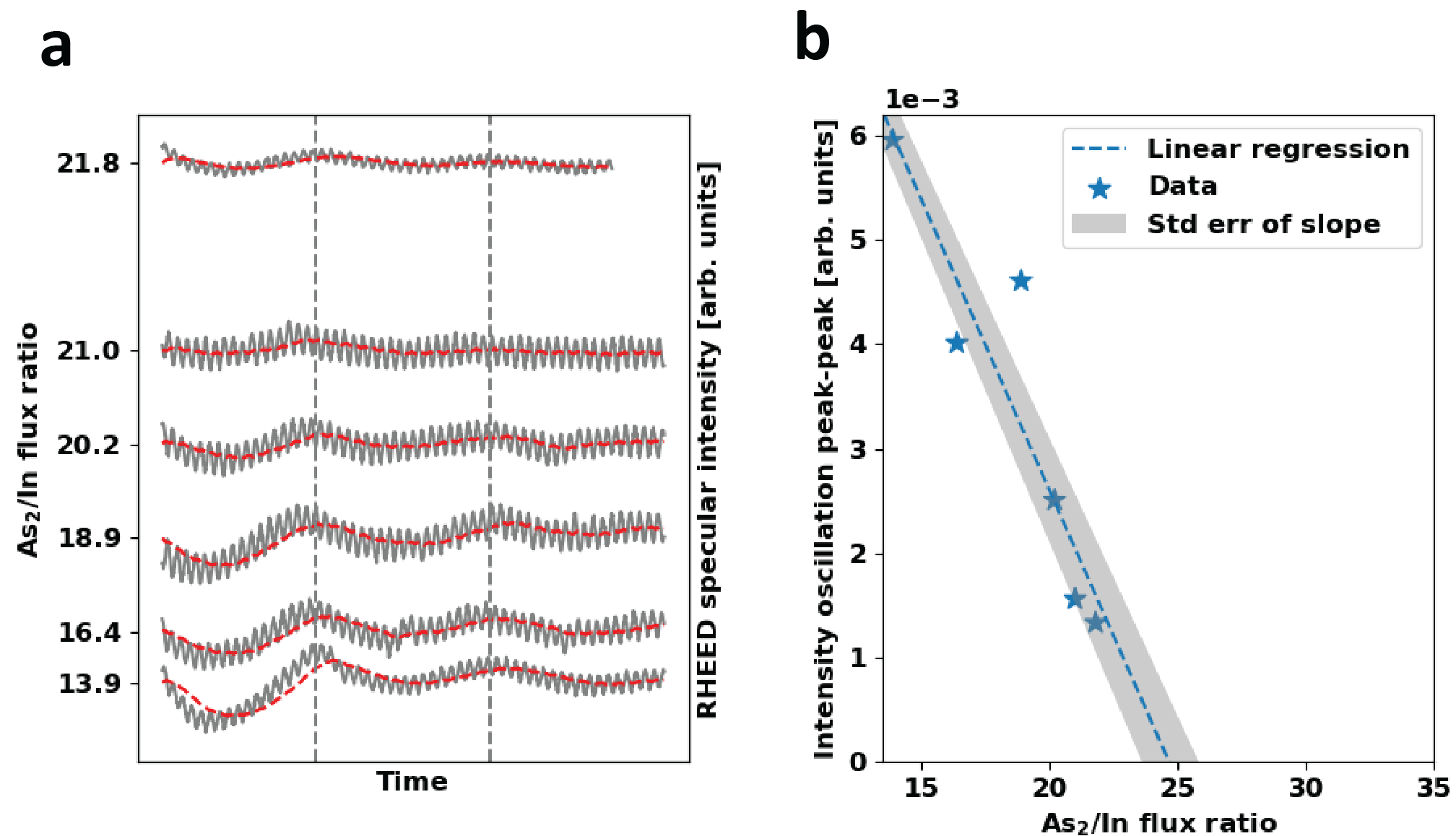
The growth parameter space that results in step-flow like growth on the other hand is comparably small, involves high As to In flux rations and is centered around about 500∘C substrate temperature. Due to a limit to the highest achievable As flux (especially in our system but generally for all valved cracker sources) the group III limited growth rate must be kept low (below 0.1 ML/s) to enable these high As2/In flux ratios which is coincidentally to the benefit of the quality of the grown surfaces 6 but might post a drawback for device fabrication. We experimentally probed the transition from step flow like growth to the onset of 2D nucleation by the appearance of RHEED oscillations upon ramping down the As flux at a fixed substrate temperature. The lack of a sharply defined transition was attributed to the low growth rates and subsequent low response time of the RHEED signal. At 0.06 ML/s formation of a single ML takes 16.6 seconds which is difficult to detect in the RHEED signal. Figure 7 shows the results of such a RHEED oscillation series for the most relevant substrate temperature (Tsub) of 500∘C. It can be observed that the maximal observed peak to peak oscillation amplitude in Figure 7a decreases with increasing As2/In flux ratio. When plotted against each other as shown in Figure 7b and extended to zero we gain a range of As2/In flux ratios of the transition region to step flow growth mode centered around the conditions for which we found the smallest roughness values.
7.2 Balance Line Detection
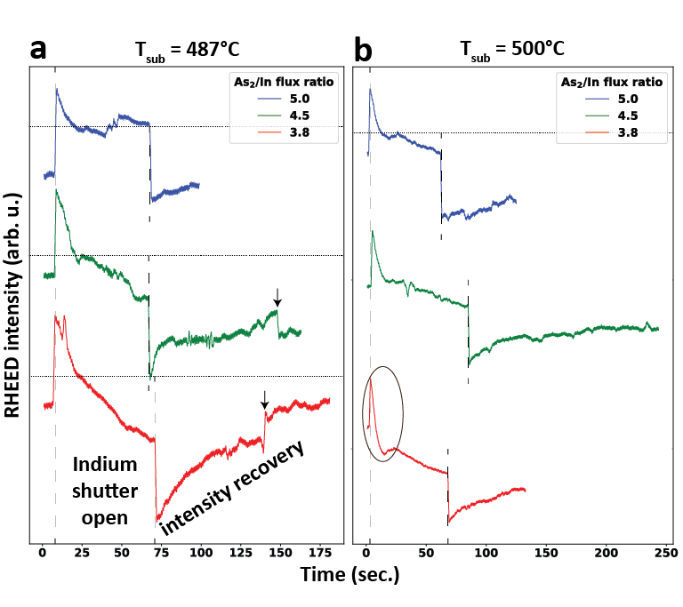
The so-called detailed balance line for the InAs(111)A homoepitaxy is the border in the growth parameter space between group V and group III limited growth regimes. With increasing substrate temperature the arsenic will first start desorbing from the InAs(111)A surface from about 350∘C on and from about 520∘C on indium atoms will also start absorbing. Therefore, two regimes should be expected. An exponential increase in arsenic flux is needed from 350∘C to 520∘C to stabilize the surface, after which a stark increase would be expected to be needed to furthermore counter indium desorption, in other words, bury the surface to stabilize it. The balance line for InAs(111)A was recorded by RHEED intensity measurements by Nomura et al. already in 1995 37. To confirm the validity of this data for the MBE in this study, we repeated such measurements for two points of the substrate temperature (478 and 500∘C) and three As2/In flux ratio values, which should be crossing the balance line. We indeed found a change from almost constant RHEED intensity during a short growth period to a decrease in intensity as presented in Figure 8. Horizontal dotted lines show the level of RHEED intensity ignoring the typical initial growth related decrease in intensity, marked by a solid oval in Figure 8b after opening the In-shutter to grow approximately 5 ML of InAs(111)A at a rate of 0.076 ML/s, after which the In shutter is closed again and possible recovery of RHEED intensity is recorded. The opening and closing of the In shutter is visible in the RHEED signal as a sharp increase and decrease in intensity, respectively and is marked additionally with dashed vertical lines. Arrows in Figure 8a mark often observed shifting artifacts in the data that could not be assigned an origin. By these considerations, we estimate the balance line to be located between As2/In flux ratios of 4.5 and 5 at TC and slightly above 5 for TC in good agreement with the Nomura data set where the respective values are 4.8 and 5.5.
8 Optical Microscopy
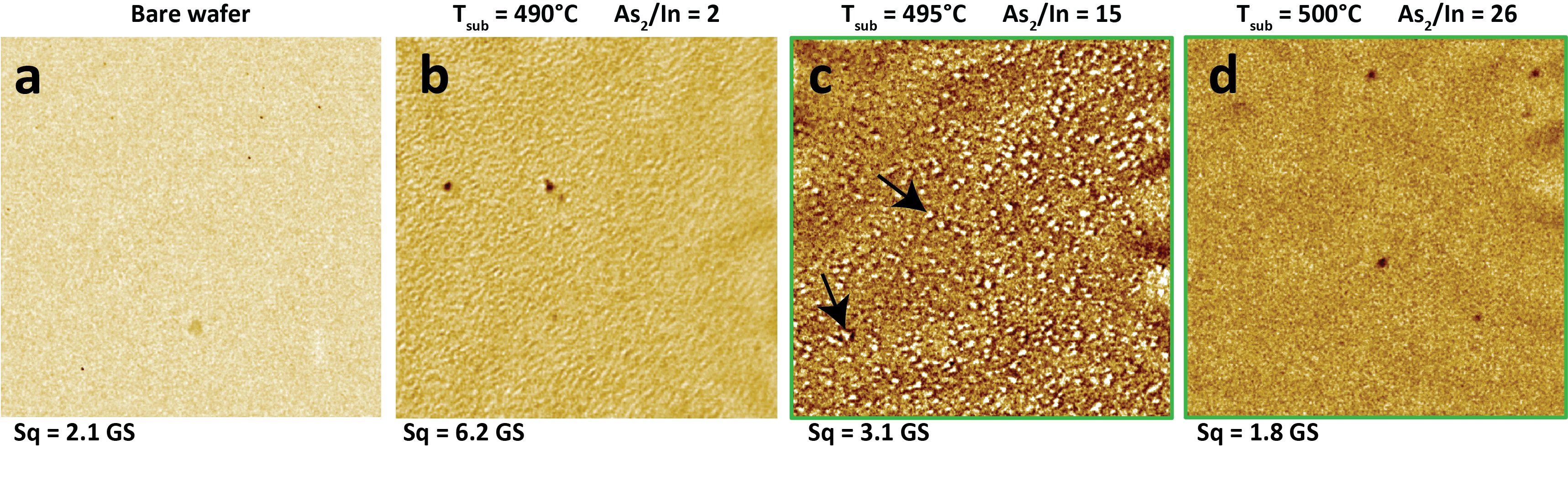
In order to determine the growth quality at a much larger scale, optical microscope (OM) images were taken with the optical microscope which is aiding cantilever placement in the Bruker Dimension Icon AFM. They represent the respective areas where AFM scans where taken. Figure 9b-d contains OM images for the first three samples in the As2/In flux ratio series. And Figure 9a an OM image of an epi-ready wafer surface. Grey-scale (GS) surface roughness values are extracted and show that the large scale optimal surface 9d is smoother than the bare epi-ready wafer. The wavy features are artifacts from the imaging of the AFM cantilever and of similar strength for all OM shown. Figure 9c has the highest amount of widely distributed sharply protruding hillocks, as marked by arrows, which could be the reason for the atomically clean surfaces in between, assuming adatoms preferentially are include in the hillocks.