Plasmonic Transverse Dipole Moment in Chiral Fermion Nanowires
Abstract
Plasmons are elementary quantum excitations of conducting materials with Fermi surfaces. In two dimensions they may carry a static dipole moment that is transverse to their momentum which is quantum geometric in nature, the quantum geometric dipole (QGD). We show that this property is also realized for such materials confined in nanowire geometries. Focusing on the gapless, intra-subband plasmon excitations, we compute the transverse dipole moment of the modes for a variety of situations. We find that single chiral fermions generically host non-vanishing , even when there is no intrinsic gap in the two-dimensional spectrum, for which the corresponding two-dimensional QGD vanishes. In the limit of very wide wires, the transverse dipole moment of the highest velocity plasmon mode matches onto the two-dimensional QGD. Plasmons of multi-valley systems that are time-reversal symmetric have vanishing transverse dipole moment, but can be made to carry non-vanishing values by breaking the valley symmetry, for example via magnetic field. The presence of a non-vanishing transverse dipole moment for nanowire plasmons in principle offers the possibility of continuously controlling their energies and velocities by the application of a static transverse electric field.
I Introduction
Plasmons are fundamental excitations of metals, in which electronic charge oscillates against the fixed positively charged background of a material, with accompanying electric fields that allow for self-sustaining collective motion Pines and P.Noziéres (1966); Bohm and Pines (1953); Giuliani and Vignale (2005); Kittel (2004). The behavior can be understood at a semiclassical level, by solving Maxwell’s equations in the presence of a frequency-dependent conductivity, which encodes information about the electron dynamics in the material Dressel and Grüner (2002). Beyond their bulk realization, plasmons may be confined to the surfaces of some solids, with charge oscillations whose amplitudes evanesce quickly inside the material Ritchie (1957); Pitarke et al. (2006). The development of two-dimensional electron systems in semiconductors Ando et al. (1982) allowed such confined plasmons Stern (1967); Das Sarma (1984) to be realized with a degree of tunability not possible at the surface of a bulk material. In more recent years, the advent of van der Waals materials, particularly graphene, has greatly enriched the set of interesting physical possibilities for two-dimensional plasmons Wunsch et al. (2006); Hwang and Das Sarma (2007); Grigorenko et al. (2012); Luo et al. (2013); Yu et al. (2015); Gonçalves and Peres (2016). These include a myriad of applications and phenomena, in areas as diverse as terahertz radiation, biosensing, photodetection, quantum computing and more Hutter and Fendler (2004); Sekhon and Verma (2011); Nikitin et al. (2011); Thygesen (2017); Agarwal et al. (2018); Linic et al. (2011); Ju et al. (2011); Suárez Morell et al. (2017); Stauber et al. (2020a); Woessner et al. (2015); Alcaraz Iranzo et al. (2018); Giri et al. (2020); Ni et al. (2015); Brey et al. (2020).
Beyond all this, plasmons are interesting for basic physical reasons: they represent quantum, bosonic excitations of charged fermions with a Fermi surface Sawada et al. (1957); Gell-Mann and Brueckner (1957). Their quantum nature can in principle become evident through manifestations of their quantum geometry. In two-dimensional materials this nature becomes particularly important because it makes possible strong light-matter interactions, allowing for probes well below the wavelength of light at plasmonic frequencies Tame et al. (2013); Fitzgerald et al. (2016); Bozhevolnyi and Khurgin (2017); Zhou et al. (2019). Moreover, Berry curvature in the electronic structure of the host material may lead to chiral behavior even in the absence of a magnetic field Song and Rudner (2016). More generally quantum effects may lead to non-reciprocal behavior of plasmons Shi and Song (2018); Papaj and Lewandowski (2020). Indeed, in some systems plasmons have internal structure in the form of a static dipole moment, which leads to non-reciprocity in their scattering from point impurities or other circularly symmetric scattering centers Cao et al. (2021a). This quantum geometric dipole (QGD) moment is present in collective excitations of insulators – excitons – as well Cao et al. (2021b). In both cases, the QGD is transverse to the momentum of the collective mode.
An interesting question is whether effects of this transverse dipole moment can be directly observed, independent of its impact on scattering. One way to approach this question is to consider its effect on plasmons in a confined geometry, which may tend to orient the dipole moment in a way that allows coupling to electric fields. The simplest such geometry is quasi-one-dimensional, in which one might expect the dipole moment to align perpendicular to the system cross-section. This is the subject of our study. In what follows, we consider a system that supports a plasmonic QGD, a layer of gapped chiral fermions, in which the single-particle states are confined to be within a narrow channel. Such systems arise naturally in the context of transition metal dichalcogenides (TMD’s) Xiao et al. (2012) and for graphene, which, when placed on a boron nitride or silicon carbide substrate, may develop a gap at its Dirac points as large as 0.5eV Nevius et al. (2015); Jariwala et al. (2011) The single-particle electronic structure of such nanowires is sensitive to the precise nature of their edges Bollinger et al. (2001); Brey and Fertig (2006a, b); Akhmerov and Beenakker (2008), and may or may not involve the mixing of valleys Brey and Fertig (2006a); Palacios et al. (2010). For simplicity, our studies focus on infinite mass boundary conditions Berry and Mondragon (1987) for which there is no such valley mixing.
Plasmons in nanowires of chiral fermions Brey and Fertig (2007) share many properties with those of scalar fermions Li and Sarma (1989); Hu and O’Connell (1990). Prominent among these are the presence of collective modes with an essentially linear dispersion, and gapped intersubband modes. As we explain below, for a single chiral fermion, all these modes support transverse dipole moments with magnitude proportional to the longitudinal momentum of the plasmon. This orthogonality of the dipole moment and momentum is exactly as one finds for the QGD in two dimensions Cao et al. (2021c, a). Interestingly, in these quasi-one dimensional systems it appears even when there is no intrinsic gap in the spectrum, so that the QGD vanishes in the corresponding two dimensional system Cao et al. (2021c, a), the gaps introduced by the transverse confinement stabilize the dipole moment. For systems with pairs of Dirac points connected by time reversal symmetry, the transverse dipole moment vanishes, but non-vanishing values can be introduced into their plasmons by breaking this symmetry, for example with a magnetic field. An interesting physical consequence of this physics is that this dipole moment can be coupled to a transverse electric field Pizzochero et al. (2021), allowing a degree of continuous control over the plasmon frequency and velocity that is unavailable in other nanowire systems.
This article is organized as follows. In Section II we discuss the single-particle wavefunctions for the confined states, and, when appropriate, for edge states of the massive chiral fermions we consider, assuming infinite mass boundary conditions. Section III is devoted to a discussion of how we derive plasmon spectra and the dipole moments associated with them. This is followed by a description of our numerical results in Section IV. In Section V contains a summary and discussion of our results. Our paper also contains three appendices. Appendix A presents further details of how the single particle states are derived. In Appendix B demonstrate that there are multiple gapless plasmon modes in the systems we consider, focusing on the case of a system with two occupied transverse states as an example. Finally, Appendix C presents a an explicit expression for the plasmon transverse dipole moment that is specifically appropriate for infinite mass boundary conditions.
II Chiral Fermions on a Nanowire: Single Particle States
We begin by deriving the single-particle states for our nanowire models. The Hamiltonian we adopt for the non-interacting system in two dimensions is
| (1) |
where indicates a valley degree of freedom, here in TMD materials corresponds to the () valley. We have adopted units such that , where is the velocity of the chiral particles in the absence of the mass parameter . Its spectrum has a gap . This Hamiltonian is an appropriate long-wavelength description of TMD materials when excitations involving spin flips are ignored, and in the limit it also describes the single particle physics of graphene Castro Neto et al. (2009); Xiao et al. (2012); Katsnelson (2012). Eigenstates of consist of right-and left-moving solutions in the -direction,
with energies
| (2) |
We choose an orientation in which the electrons are confined in the direction and are free to move along . To confine the electrons, we adopt for simplicity infinite mass boundary conditions Berry and Mondragon (1987),
| (3) |
where is the sign of the Chern number outside the wire, and in writing this we have assumed . (Details of how one arrives at Eq. 3 are presented in Appendix A.) Note that, without loss of generality, we may assume a Chern number (of magnitude Girvin and Yang (2019)) for each valley in the material (i.e., inside the wire) with the sign of given by . This choice of boundary condition has the advantage of admitting confined solutions without admixing valleys, but the resulting confined states depend on their momentum along the wire. This latter property is generic for chiral fermions Brey and Fertig (2006a, 2007); Akhmerov and Beenakker (2008), although in the special case where there are only two valleys, with equal momentum components along the wire direction, this momentum dependence is lifted Brey and Fertig (2006a) (at the cost of admixing valleys.) The momentum dependence of the confined wavefunctions is a significant difference from the typical situation for electrons with scalar single-particle states Li and Sarma (1989). Note that the parameter enters the boundary condition because one must choose the mass term outside the wire to tend to either or , and the choice of this sign determines whether the wire supports edge states, as we discuss further below.
Eigenstates of which satisfy the boundary conditions have the form (see Appendix A)
| (4) |
with
| (5) |
| (6) |
with a normalization constant given by
| (7) |
in which and are the length and the width of the wire respectively. The allowed values of satisfy the transcendental equation
| (8) |
which in turn quantizes their values,
| (9) |
where
In addition to these confined states, there may also be edge states, depending on the relative sign of the wire and the vacuum Chern numbers. In systems with time reversal symmetry, these come in pairs on each edge running in opposite directions, with the member of each pair associated with one or the other valley. For systems with a single chiral fermion, for which time reversal symmetry is necessarily broken, a single edge state is present on each edge. These edge states exist only when the wire material and vacuum are topologically distinct, i.e. the signs of their Chern numbers are opposite,
| (10) |
The edge states correspond to evanescent solutions of the Hamiltonian equation (see Appendix A), with wavefunctions
| (11) |
and
| (12) |
| (13) |
and energy
| (14) |
In these expressions the evanescent wave vector satisfies the transcendental equation
| (15) |
Note that Eq. 15 only has solutions when the wire is wider than a minimal value (), given by
| (16) |
where we have replaced the explicit functional dependence on . Examples of the single particle dispersions relevant to our model are given in Figs. 1(a) and 1(b).
III Plasmon Wavefunctions, Energies, and Dipole Moments
In our study we are interested in the intrinsic dipole moment of plasmon states of a one dimensional channel. Most previous studies of these focus on the dielectric function, as computed in the random phase approximation (RPA) Li and Sarma (1989); Das Sarma and Lai (1985); Li and Das Sarma (1991). This reveals the plasmon frequencies and their impact on the charge response of the system to applied electric fields. For our purpose we need access to the plasmon wavefunctions. The approach we adopt casts the plasmon wavefunction as a linear combination of particle-hole excitations around a Fermi sea ground state. While equivalent to RPA, it is best understood as a time-dependent Hartree approximation. In this section we explain how this approach is implemented and how the intrinsic transverse dipole moment may be extracted from it.
III.1 Hamiltonian and Plasmon Raising Operator
Our Hamiltonian is a sum of single particle and interaction parts, . The first of these is
| (17) |
where creates an electron in subband with longitudinal momentum , with valley and spin indices and , respectively. is the single particle energy, as computed in the previous section. For the interaction term we write
| (18) |
where the (vector) field operator creates an electron of spin in the two orbitals of the chiral fermion system at the location , and denotes normal ordering of an operator . Expanding in the single particle wire states,
| (19) |
brings the interaction to a form which may be written as
| (20) |
where . In writing this we have taken note of the fact that for each subband there is a single quantized transverse momentum magnitude, , whose states with positive and negative values are admixed to form the transverse states discussed in the last section. Identifying , this allows us to adopt a simplified indexing for the annihilation operators, .
In what follows we adopt a contact interaction . This yields intrasubband plasmon modes that disperse linearly with longitudinal plasmon momentum . If a potential is instead used, one expects to find for at least one gapless plasmon mode; however in practice the divergence of the slope is extremely difficult to see Li and Sarma (1989). Thus the contact interaction introduces significant simplification in the computation of the matrix elements, without loss of any essential qualitative behavior in the plasmon mode. In practice, we choose the value of to match results for the slope of a plasmon mode as computed using the Coulomb interactions in a graphene system Karimi and Knezevic (2017).
Collective excitation of the system can be obtained from operators satisfying the equation THOULESS (1961); Sawada et al. (1957)
| (21) |
In general analytic solutions to Eq. 21 are not available. However in the case of plasmons, corresponding to charge density excitations in the system, one may approximate the form of the plasmons raising operator as a linear combination of single particle-hole pairs Sawada et al. (1957),
| (22) |
and then treat the commutator in the time-dependent Hartree approximation,
| (23) |
Together with the commutator involving the single particle Hamiltonian , one arrives at an eigenvalue equation for the particle-hole weights and the plasmon frequency ,
| (24) |
In this work we work strictly in the zero temperature limit, so that if the state is occupied (unoccupied) in the ground state.
We solve Eq. III.1 numerically by retaining a discrete set of points in the sum, so that it becomes a matrix eigenvalue equation. Because we are interested in the lowest lying plasmon modes, we further simplify the equation by retaining only intra-band particle-hole excitations, so that we take only when ; we have verified that keeping inter-subband excitations has little effect on our results. We have further verified that increasing the number of points used for the results reported below have little effect on them.
III.2 Plasmon Dipole Moment
In previous work Cao et al. (2021c, a) we demonstrated that two-body excitations, including excitons and plasmons, may carry an internal dipole moment that is tied to the quantum geometry of their wavefunctions. One sees this by defining Berry connections specific for the electrons (=1) and holes (=2),
with
where is the wavefunction of the excited state. These connections can be directly related to the average electric dipole moment of a plasmon,
| (25) | |||||
where is the quantum geometric dipole. This quantity is relevant to plasmons because they may be understood as particle-hole excitations around a Fermi surface. In a two-dimensional system one finds is orthogonal to , and for small it is linear in . This geometry suggests that when plasmons carry a non-vanishing in a two-dimensional material, plasmons confined to a one-dimensional channel of the same system may carry a transverse dipole moment. We can check this by computing the plasmon dipole moment directly. For a wire oriented along the -direction, following the reasoning above, for a plasmon state with momentum along the wire one may write
| (26) |
Recalling the notation above in which a vector specifies an electron state with longitudinal momentum in a transverse state , we write , yielding an explicit expression,
| (27) |
In our numerical calculations, Eq. III.2 is used to compute the dipole moment of a plasmon state. As we shall see, one finds that plasmons of a single chiral Dirac fermion nanowire generically have non-vanishing , but with increasing wire width, this vanishes unless the corresponding two-dimensional system has a non-vanishing quantum geometric dipole.
IV Results
In this paper we focus on intraband plasmons, which for our contact interaction disperse linearly with momentum from zero energy. In general we find that the number of such gapless plasmon modes is equal to the number of subbands which cross the Fermi energy, all of which may carry non-vanishing transverse dipole moments. We begin by considering the computationally simplest case of a single chiral fermion flavor. In principle such a system might be created on the surface of a topological insulator infused with ferromagnetically ordered dopants that gap the surface states everywhere except in a narrow channel, where plasmons can be hosted. We discuss more common cases involving nanoribbons of van der Waals materials further below, for which the effects of multiple valleys and time-reversal symmetry have important consequences.
IV.1 Single Chiral Fermion
Our model Hamiltonian for a single chiral fermion is , with and given by Eqs. 17 and 18, respectively, in which only a single valley flavor is retained. For such systems we need to choose whether the vacuum outside the same system has the same or opposite Chern number as the one-dimensional system, i.e. whether or , as discussed in Section II. This determines whether the wire hosts edge states. For the realization described above one may toggle between the two cases by flipping the direction of the magnetic impurities defining the channel. The qualitative behavior of the system turns out to be the same irrespective of whether the wire hosts edge states.
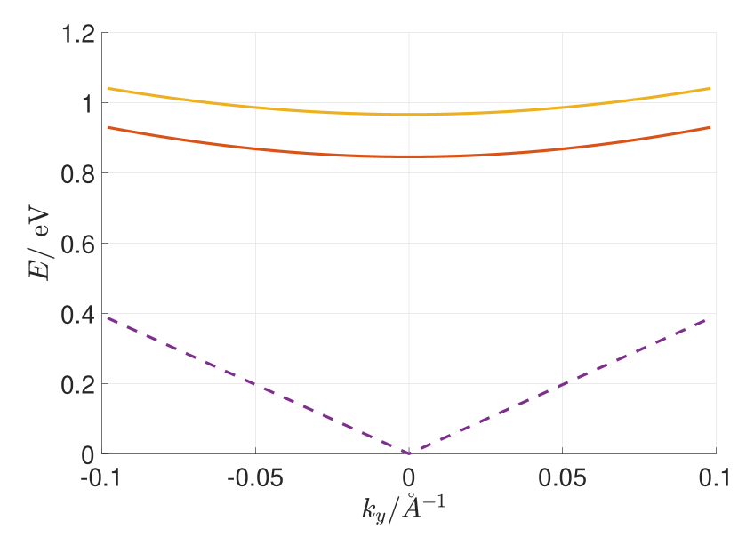
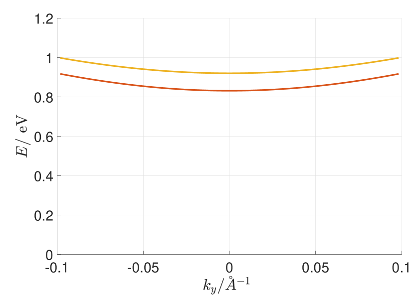
We begin with typical results, illustrated in Figs. 2(a) and 2(b) for boundary conditions in which there are no edge states (.) One observes several gapless plasmons, which at long wavelengths disperse linearly with momentum, as expected for this model. The gapless modes illustrated all lie above the energies of the particle-hole continuum. In general, the number of gapless modes is equal to the number of occupied subbands; we demonstrate this explicitly for the case of two occupied subbands in Appendix B. Importantly, all the plasmon modes exhibit non-vanishing transverse dipole moments, with magnitudes proportional to the plasmon momentum. As we discuss below, while this behavior is consistent with the (two-dimensional) quantum geometric properties of the system hosting the wire, it can be present in the wire geometry even when absent in the corresponding two-dimensional system. We also find that such qualitative results are unaffected by edge states (), as illustrated in Figs. 2(c) and 2(d); the transverse dipole moment does not appear to depend on this aspect of the system topology.
(a) 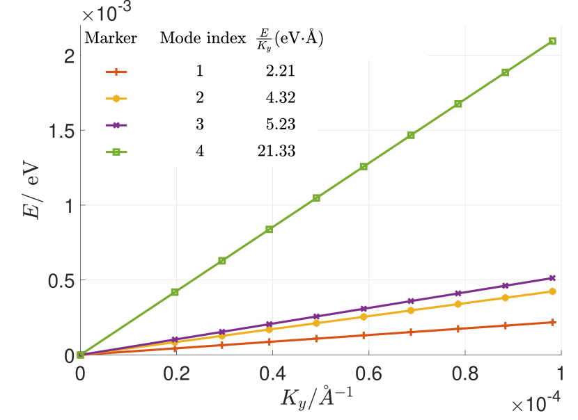 (b)
(b) 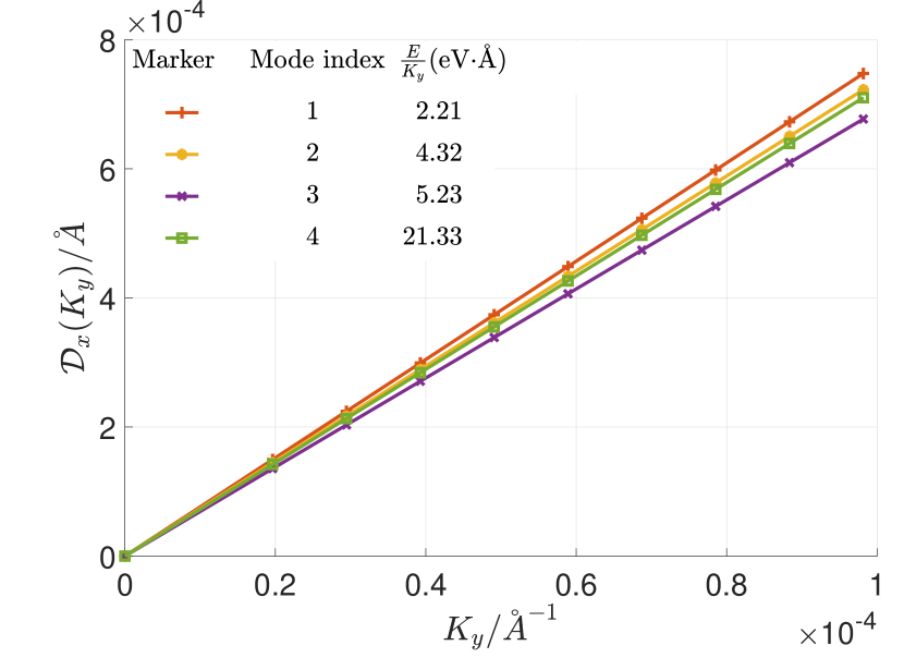
(c) 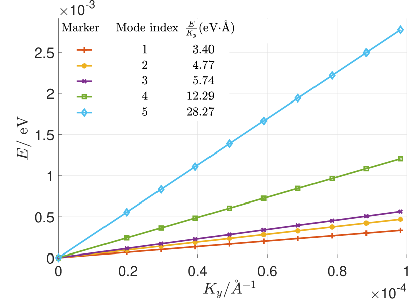 (d)
(d) 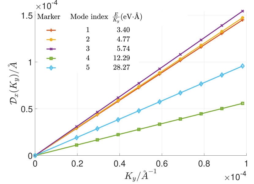
Surprising behavior of the transverse dipole moment emerges for systems with relatively large gaps. Fig. 3(a) illustrates such a case, in which the Hamiltonian parameters have been chosen to model a single valley of WSe2 Xiao et al. (2012), and (no edge states on the wire). Fig. 3(b) illustrates the transverse dipole moment of these plasmon modes. Remarkably, one finds essentially the same value for all the modes. This can be understood by close examination of the expression for the plasmon dipole for small momentum , which we show in Appendix C to have the form
| (28) |
where is the quantized transverse momentum of the subband. Note that in this expression, in the present case where we consider a single valley (indexed by ), one may set . In situations where the gap parameter is large, the last term in the denominator becomes negligible, so that the remaining sum is determined only by the normalization of the plasmon wavefunction, and the resulting dipole moment becomes independent of the specific plasmon mode.
Figs. 3(c) and 3(d) illustrate the corresponding results for the same parameters, but with . In this case the systems hosts edge states in addition to the confined single-particle states, so that there are five occupied subbands. Here all but one of the plasmon modes host the same non-vanishing dipole moment, while the remaining mode does not. The result again can be understood from Eq. 28. In this case one finds that the mode with vanishing dipole moment has nearly all its weight in the edge state, for which , so that the denominator becomes divergent. More physically, because of the relatively large gap, the penetration length of the edge state into the bulk becomes independent of , as does the single-particle transverse wavefunction. In this case the plasmon cannot sustain a transverse dipole moment. It is interesting to note that the difference in behaviors apparent in Figs. 3(b) and 3(d) in principle offers an interesting way to distinguish when the one-dimensional channel is in a topological setting from a situation in which it is not: with the application of a transverse electric field coupling to the dipole moment, the energies and corresponding velocities of all the plasmon modes would shift in the non-topological case, whereas in the topological case one of these modes will be insensitive to the electric field.
While the presence of an intrinsic dipole moment associated with plasmons in these one-dimensional systems is consistent with the presence of a QGD in their two-dimensional realizations Cao et al. (2021a), it is not necessary for for these one-dimensional plasmons to carry a transverse dipole moment. Figs. 4(a) and 4(b) illustrate this for the situation in which the gap parameter vanishes, so that for plasmons in this system in two dimensions Cao et al. (2021a). Clearly one finds a non-vanishing transverse dipole for such plasmons, and indeed the results are qualitatively similar to those found for . Note that one does not expect the one-dimensional system to host edge states when .
(a) 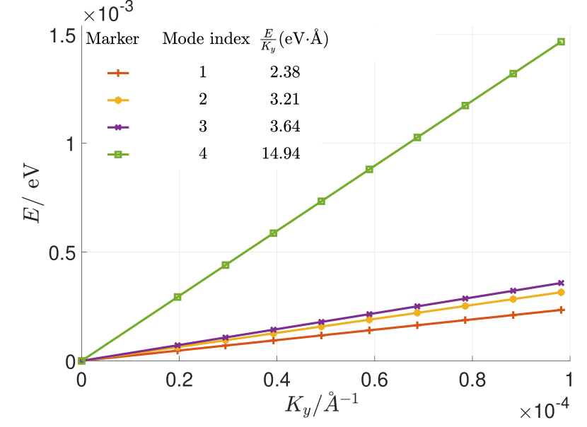 (b)
(b) 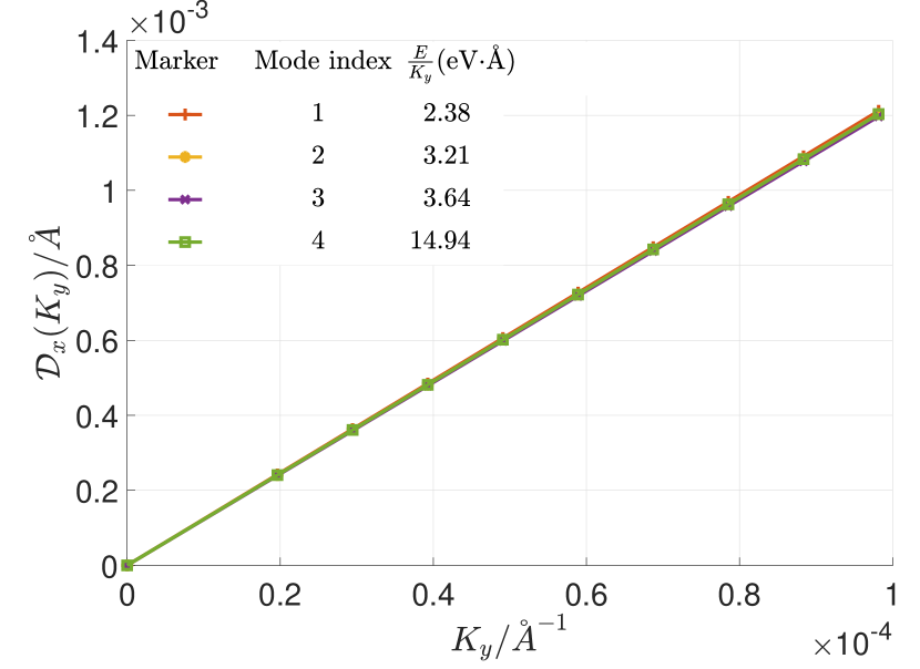
(c) 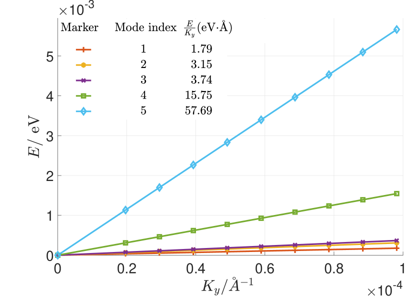 (d)
(d) 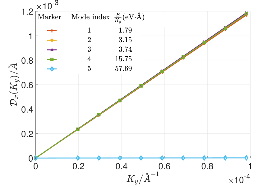
(a) 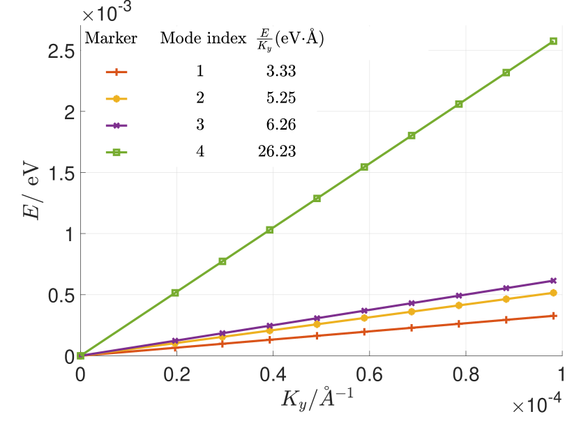 (b)
(b) 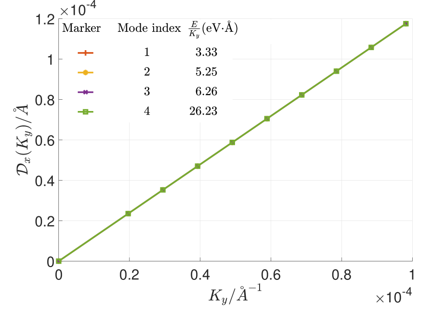
While for these relatively narrow systems we see little difference in the behavior of one-dimensional plasmons between systems in which and , the distinction becomes relevant as the conducting channel gets wider. We illustrate this by computing the plasmon transverse dipole moment both for a chiral fermion system with vanishing gap (), for which Cao et al. (2021a), and for a gapped chiral fermion, for which it does not, and examine the plasmon behavior as the width increases while the Fermi energy is held fixed. Fig. 5(a) illustrates the behavior of the velocity of the fastest plasmon for a system with , and the associated dipole moment can be seen to vanish as becomes large (Fig. 5(b)). Figs. 5(c) and 5(d) illustrate the corresponding quantities for a system with , for which the transverse dipole moment matches onto the (two-dimensional) quantum geometric dipole magnitude . The robustness of the plasmon dipole moment with increasing is thus a signature of its quantum geometric nature.
(a) 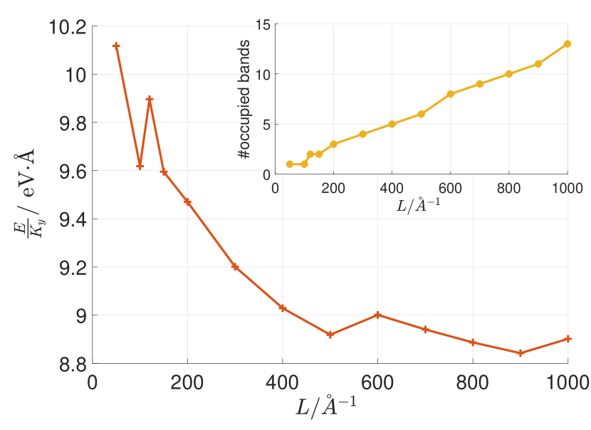 (b)
(b) 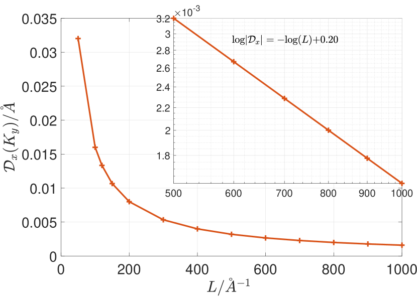
(c) 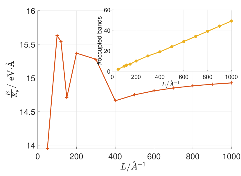 (d)
(d) 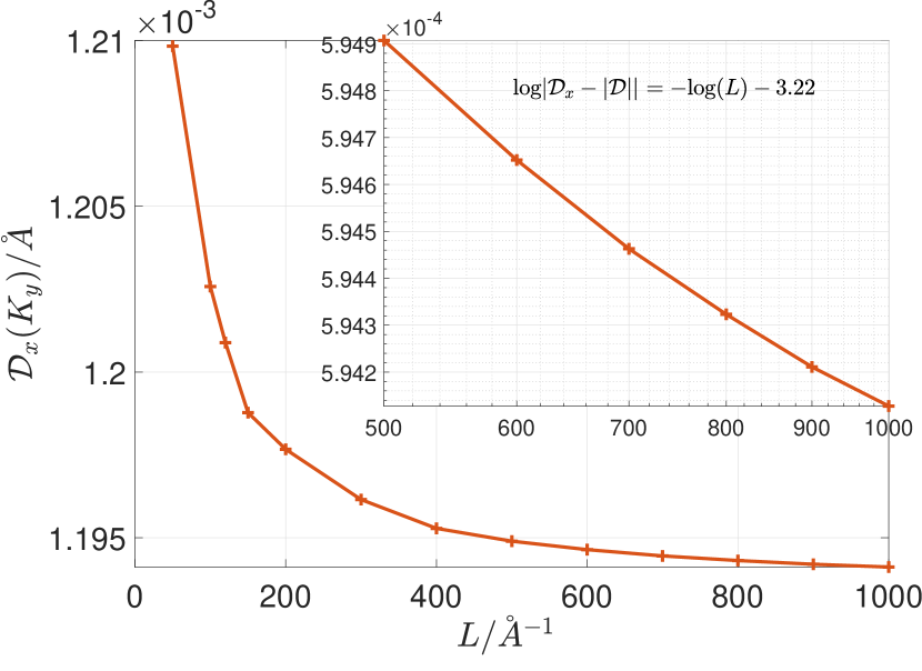
IV.2 Mulitple Valleys: Vanishing Dipole for Time-Reversal Symmetric Systems
While the systems discussed above involve relatively simple Hamiltonians, their physical realizations require time-reversal symmetry-breaking, for example via ferromagnetic insulating films which would need to be patterned onto the surface of a topological insulator. A much simpler system to realize would be a nanoribbon of transition metal dichalcogenide (TMD) material, which in most cases preserves time reversal symmetry. Such systems typically have two valleys, which are time-reversal partners of one another. With time-reversal symmetry intact, one does not expect plasmon modes to carry an intrinsic dipole moment. Figs. 6(a) and 6(b) illustrate such a situation.
(a) 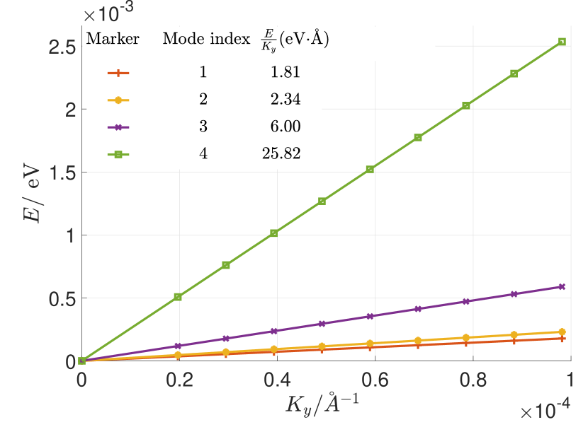 (b)
(b) 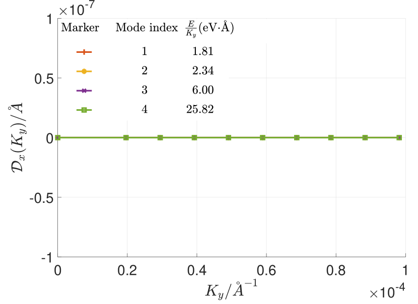
(c)  (d)
(d) 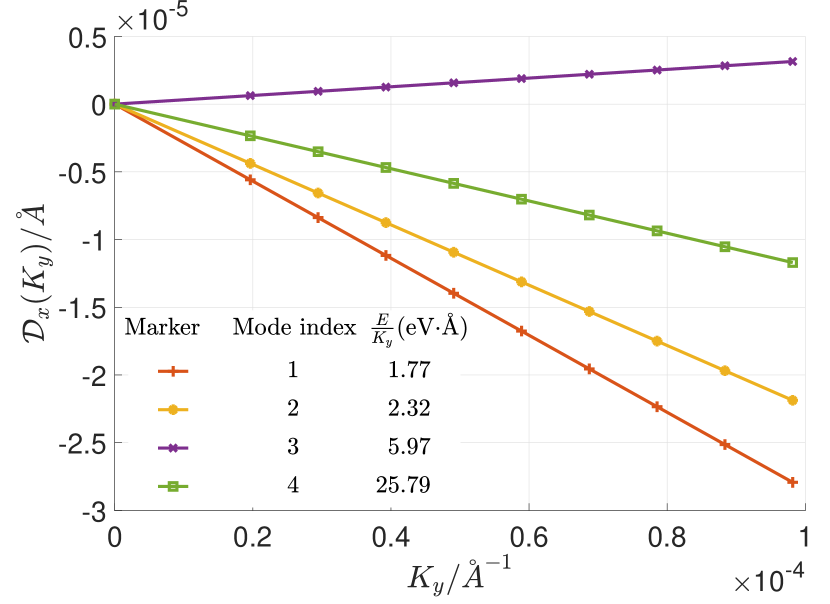
Non-vanishing dipole moments in such systems can be induced by breaking the symmetry between valleys. In TMD materials, spin-orbit coupling leads to a splitting between spin-up and spin-down states in opposite directions for the two valleys Xiao et al. (2012), so that a magnetic field imbalances the populations of the valleys through the Zeeman coupling. For magnetic fields that are not too large, such that the magnetic length , with the magnetic field, is larger than the ribbon width, the orbital motion of the electrons will largely be unaffected by the field. To a good approximation one then only needs to include the spin dependence of the Fermi surfaces to account for the field.
Figs. 6(c) and 6(d) illustrate such a situation in a ribbon of width Å, for system parameters modeled after the hole bands of WSe2, with a magnetic field T, for which Å. While the bands for each valley have the same dispersion, the Zeeman coupling leads to a difference of meV in the extrema of the and bands, yielding different carrier populations in each of them. While this leads to little change in the plasmon dispersions (compare Figs. 6(a) and 6(c)), the plasmons now carry dipole moments with small magnitudes (Fig. 6(d).) Interestingly, these dipole moments can have either sign. At the more extreme end, this effect can used to completely depopulate one of the valleys of carriers. This situation is illustrated in Figs. 7(a) and 7(b). Interestingly this yields a plasmon dipole moment that is relatively large.
(a) 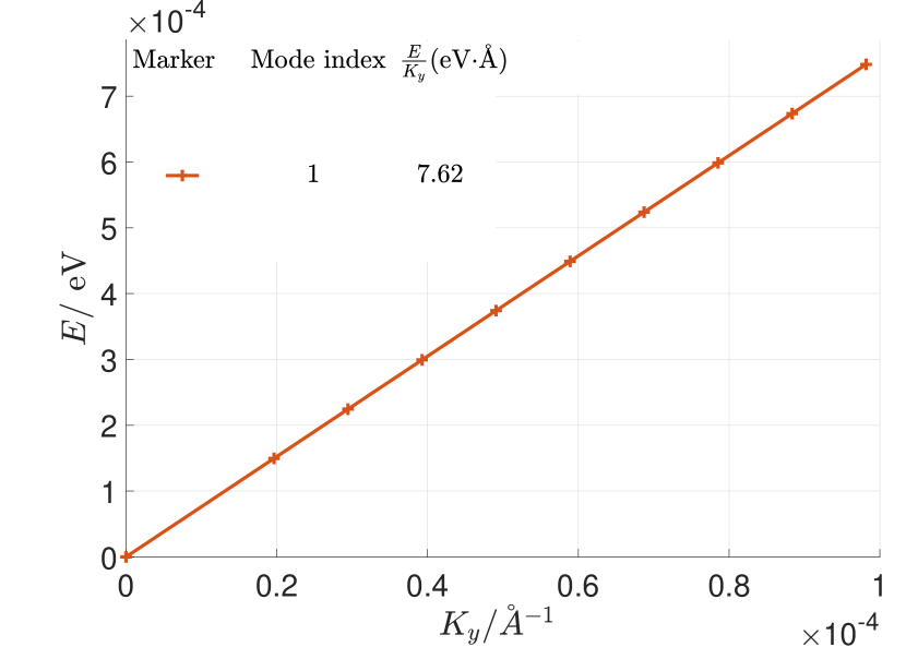 (b)
(b) 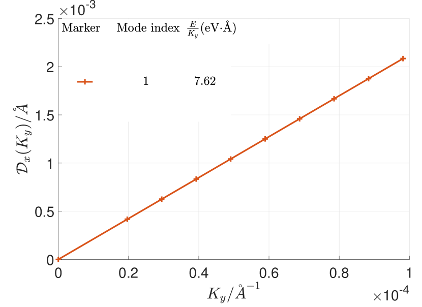
V Summary and Discussion
In some two-dimensional conducting systems, plasmon excitations come with an intrinsic dipole moment that is quantum geometric in nature Cao et al. (2021a). In this work, we have explored conditions under which this kind of dipole moment might be found for quasi-one-dimensional geometries of the corresponding systems, using an RPA approach. Our studies focused on chiral fermions, as might be found on the surface of a topological insulator, or in two-dimensional van der Waals materials such as graphene or TMD’s, and we adopted a simplified model with infinite mass boundary conditions at the system edges. We found that the presence of a transverse dipole moment is more ubiquitous in the wire geometry than in the two-dimensional system: the opening of a gap in the spectrum due to transverse confinement is sufficient to stabilize it, even when the corresponding gapless spectrum has no such dipole moment in two dimensions. The connection with the quantum geometric dipole is made by considering the wide wire limit, for which the plasmons retain dipole moments when the corresponding two dimensional system has a non vanishing quantum geometric dipole.
These plasmons differ from the corresponding modes of more conventional semiconducting quantum wires (e.g., GaAs): the topological character of the chiral fermions allow the possibility that they support edge states, which we find are present for sufficiently wide wires. Their presence increases the number of gapless plasmon modes supported by the systems, but they only differ in their qualitative behavior for systems with relatively large gaps. In this limit we found that the dipole moments of the plasmon modes supported by the transverse confined states became degenerate across the modes, whereas a single plasmon associated with the edge states has vanishing dipole moment.
Single chiral fermion flavors can only be found in systems with broken time-reversal symmetry. In principle a conducting channel of these could be fabricated on the surface of topological insulator with ferromagnetically ordered magnetic ions on it surface, with a one-dimensional channel cut through. Systems with both chiral fermions and time-reversal symmetry support multiple flavors of chiral fermions (valleys), which are time-reversal partners of one another. Plasmons in these systems do not carry dipole moments. However in TMD’s they can be induced by the introduction of a magnetic field, which due to spin-orbit coupling imbalances the carrier populations in different valleys. For low carrier densities one may find complete depletion of some valleys, leading to relatively large transverse dipole moments in the plasmons.
A transverse dipole moment associated with a plasmon in a nanowire will in principle be signaled by a sensitivity of its frequency and speed to the application of a transverse electric field Pizzochero et al. (2021): these will both vary linearly with electric field. For example, for the system parameters considered in Figs. 7(a) and 7(b), an external electric field of 0.01 VÅ-1 will modify the speed of the plasmon by approximately m/s, and its energy by approximately 3%. Control of plasmon energies in such a continuous way in a single system could in principle bring new capabilities to plasmonic systems incorporating such nanowires.
Our studies suggest further directions for exploration. Beyond the gapless plasmons we have focused on in this work, nanowires support gapped, intersubband plasmons at higher frequencies Li and Sarma (1989). Preliminary work Cao et al. indicates that these also obtain non-vanishing dipole moments in chiral fermion settings, and they offer a way to detect this physics at higher frequencies. One may also consider the presence and role of transverse dipole moments in more complicated settings than considered in this work. For example, understanding the behavior of nanowire plasmons for other classes of boundary conditions, in particular those for which valley mixing is induced at the single-particle level Brey and Fertig (2006a); Akhmerov and Beenakker (2008), would likely be important for many types of nanowires. One may also consider the effects of transverse dipole moments on plasmon nanochannel networks, which arise naturally in moiré superlattices, and which have been shown to support their own unique dynamics Ni et al. (2015); Brey et al. (2020); Stauber et al. (2020b). Such systems under some circumstances may become spontaneously valley-polarized, opening another avenue for the broken time-reversal symmetry needed for transverse dipole moments.
Plasmon modes can be generally understood as collective oscillations of the electric dipole moments of conducting systems. That such oscillations can occur with a static component which depends on the plasmon momentum is a relatively new insight, allowing the possibility of new physical phenomena. Nanowires offer a setting in which the direction of these dipole moments are fixed, so that they can be interrogated with electric fields. For systems that support them, we expect they will admit new plasmonic phenomomena of fundamental interest.
Acknowledgements
L.B. acknowledges funding from PGC2018-097018-B-I00 (MICIN/AEI/FEDER, EU). HAF and JC acknowledge the support of the NSF through Grant Nos. DMR-1914451 and ECCS-1936406. HAF acknowledges support from the US-Israel Binational Science Foundation (Grant Nos. 2016130 and 2018726), of the Research Corporation for Science Advancement through a Cottrell SEED Award.
Appendix A: Nanowire with Infinite Mass Boundary Condition
In order to model chiral Dirac fermions confined to a quasi-one-dimensional channel, we consider a two-dimensional system with a position-dependent mass term,
The Hamiltonian of the system is, in general,
where is the valley index. We find stationary states by matching eigenstates of in the regions (region ), (region ) and (region ) at the locations and . We ultimately take the limit (infinite mass boundary conditions Berry and Mondragon (1987)), but some care must be taken with regard to whether the Chern numbers in the central and outer regions are the same or different. These Chern numbers are given by , so that the two cases are distinguished by the sign of . For the regions outside the nanowire, we denote the sign of the Chern numbers by . Outside the wire one has for region I
with where is the energy of the state, while in region III,
with Writing the upper and lower components of the spinors as and , respectively, with the limit we obtain Berry and Mondragon (1987)
| (29) |
In the interior of the wire (region II), the general form of the wavefunction is
| (30) |
with and constants to be determined. Using Eqs. 29 one finds
| (31) |
and
| (32) |
These two equations are consistent provided
or equivalently,
Using Eqs. 31 and 32, one obtains the expressions
and
where is a normalization constant,
with the length of the one-dimensional region.
In addition to these confined states, the wire edges may support edge states. This can occur only if the Chern numbers of the interior and exterior regions have different Chern numbers, which occurs when
with . One finds these states by considering states that are evanescent not just in regions and but also in region . These have the form
where here . Applying Eqs. 29 gives
| (33) | ||||
| (34) |
Eliminating and in eqs. (33) and (34), we arrive at a transcendental equation for ,
| (35) |
Eq. 35 may be solved if and only if and . These are the conditions under which the quasi-one-dimensional system hosts edge states. Using Eqs. 33 and 34, the explicit forms for the coefficients turn out to be
and
Appendix B: Analytical Solution for Intraband Plasmons at Small Momentum
The appearance of multiple plasmon modes may appear surprising. In this section we show that this is to be expected, given the structure of the transverse wavefunctions for the systems we consider. To do this we first develop an alternative, equivalent formalism by which one may find the plasmon excitations, and then apply it to the simple situation of two occupied subbands to show that there is more than a single gapless plasmon mode.
V.1 Equivalent Dielectric Formalism
For simplicity, we consider a massless chiral fermion system (), which is equivalent to a single valley of graphene, for which we set . First, we start from eq. (III.1), and obtain the equivalent dielectric formalism for calculating plasmon frequency. The contact interaction matrix element may be written in the form
where the spinor coefficients and may be read off from Eq. 30, and are the quantized wavevectors defined in Appendix A. By defining
and
the interaction matrix elements can be written in the compact form
In the single valley case, the self-consistent equation for the plasmon wavefunction (Eq. (III.1)) can now be written as
Defining
and
one finds
| (36) |
The quantity may be understood as a dielectric function, with the expression inside the square brackets of Eq. V.1 representing a generalized polarization function . Non-trivial solutions to this equation must obey
V.2 Intra Subband Solutions for Two Subbands
We now show how this equation leads to multiple gapless plasmons. As a simplest concrete example we consider a massless chiral fermion system (e.g., single valley of graphene) with two subbands, both of which are occupied in the ground state, and include only intra-subband excitations in the analysis. In Eq. V.1 this entails retaining only pairs of indices satisfying and . One then has
| (37) |
The relevant spinors entering can be evaluated as
and
where and . We next note that for small , the momentum sums involve only very small intervals, so that one may set all the values of in the various and factors appearing in Eq. V.2 to their values where the subbands cross the Fermi energy, , where , with the Fermi energy and the velocity of the chiral fermion. After some algebra, one finds
Specializing to the case of just two occupied subbands, using the notation , one finds to linear order in
where , , and
| (38) |
Non-trivial solutons to Eq. 38 exist when
| (39) |
where
For small , Eq. 38 can be evaluated directly. Writing the (non-interacting) speed of a particle along the wire in an occupied subband at the Fermi energy as , for small one finds
| (40) |
Direct substitution of Eq. 40 into Eq. 39 generates a quadratic equation for in terms of , with solutions
where . Thus we generate two non-degenerate collective modes with frequencies different from those of the non-interacting particle-hole excitations.
Appendix C: Degeneracy of Transverse Dipole Moments
In Section IV-A, it was shown that under certain circumstances the transverse dipole moment can be the same for multiple plasmon modes at small , even when the frequencies of these modes are quite different. This behavior is explained by Eq. 28, in which one may see that becomes independent of the details of plasmon wavefunction when for the subbands involved in the plasmon wavefunction. (Note in Eq. 28, and have been set to 1.) In this Appendix we present some details of the derivation of Eq. 28.
Our starting point is Eq. III.2, and we consider only intrasubband particle-hole excitations in constructing the low energy plasmon wavefunctions. This means the quantities we need to focus on have the form
Writing the plasmon wavefunctions, Eq. 4, in the form
where , one finds
Reading off the forms of and from the wavefunctions in Section II, one finds
where we have set . Remarkably, these combinations are independent of ; because involves the difference of at two different values, terms involving and do not contribute to the dipole moment of the plasmon. For small , the transverse component of the dipole moment can now be written as where the sum is over occupied subbands, and
With some algebra one may show
and using this relation, after performing the integration one finds
The first term is independent of therefore does not contribute. Using
we arrive at
Thus to linear order in , the transverse plasmon dipole moment is
which is Eq. 28.
References
- Pines and P.Noziéres (1966) D. Pines and P.Noziéres, The Theory of Quantum Liquids: Normal Fermi Liquids. (1966).
- Bohm and Pines (1953) D. Bohm and D. Pines, Physical Review 92, 609 (1953), URL https://link.aps.org/doi/10.1103/PhysRev.92.609.
- Giuliani and Vignale (2005) G. Giuliani and G. Vignale, Quantum Theory of the Electron Liquid (Cambridge University Press, Cambridge, 2005).
- Kittel (2004) C. Kittel, Introduction to Solid State Physics (Wiley, 2004), 8th ed., ISBN 9780471415268, URL http://www.amazon.com/Introduction-Solid-Physics-Charles-Kittel/dp/047141526X/ref=dp_ob_title_bk.
- Dressel and Grüner (2002) M. Dressel and G. Grüner, Electrodynamics of Solids: Optical Properties of Electrons in Matter (Cambridge University Press, Cambridge, 2002), ISBN 9780521592536, URL https://www.cambridge.org/core/books/electrodynamics-of-solids/DFDDF1640793690DAFD338BFDD1A18BF.
- Ritchie (1957) R. H. Ritchie, Phys. Rev. 106, 874 (1957), URL https://link.aps.org/doi/10.1103/PhysRev.106.874.
- Pitarke et al. (2006) J. M. Pitarke, V. M. Silkin, E. V. Chulkov, and P. M. Echenique, Reports on Progress in Physics 70, 1 (2006), URL https://doi.org/10.1088/0034-4885/70/1/r01.
- Ando et al. (1982) T. Ando, A. B. Fowler, and F. Stern, Rev. Mod. Phys. 54, 437 (1982), URL https://link.aps.org/doi/10.1103/RevModPhys.54.437.
- Stern (1967) F. Stern, Phys. Rev. Lett. 18, 546 (1967), URL https://link.aps.org/doi/10.1103/PhysRevLett.18.546.
- Das Sarma (1984) S. Das Sarma, Phys. Rev. B 29, 2334 (1984), URL https://link.aps.org/doi/10.1103/PhysRevB.29.2334.
- Wunsch et al. (2006) B. Wunsch, T. Stauber, F. Sols, and F. Guinea, New Journal of Physics 8, 318 (2006), URL https://doi.org/10.1088/1367-2630/8/12/318.
- Hwang and Das Sarma (2007) E. H. Hwang and S. Das Sarma, Phys. Rev. B 75, 205418 (2007), URL https://link.aps.org/doi/10.1103/PhysRevB.75.205418.
- Grigorenko et al. (2012) A. N. Grigorenko, M. Polini, and K. S. Novoselov, Nature Photonics 6, 749 (2012), URL https://doi.org/10.1038/nphoton.2012.262.
- Luo et al. (2013) X. Luo, T. Qiu, W. Lu, and Z. Ni, Materials Science and Engineering: R: Reports 74, 351 (2013), ISSN 0927-796X, URL https://www.sciencedirect.com/science/article/pii/S0927796X13000879.
- Yu et al. (2015) H. Yu, Y. Wang, Q. Tong, X. Xu, and W. Yao, Phys. Rev. Lett. 115, 187002 (2015), URL https://link.aps.org/doi/10.1103/PhysRevLett.115.187002.
- Gonçalves and Peres (2016) P. A. Gonçalves and N. Peres, An Introduction to Graphene Plasmonics (2016), ISBN 978-981-4749-97-8.
- Hutter and Fendler (2004) E. Hutter and J. Fendler, Advanced Materials 16, 1685 (2004), eprint https://onlinelibrary.wiley.com/doi/pdf/10.1002/adma.200400271, URL https://onlinelibrary.wiley.com/doi/abs/10.1002/adma.200400271.
- Sekhon and Verma (2011) J. S. Sekhon and S. S. Verma, Current Science 101, 484 (2011), ISSN 00113891, URL http://www.jstor.org/stable/24078975.
- Nikitin et al. (2011) A. Y. Nikitin, F. Guinea, F. J. Garcia-Vidal, and L. Martin-Moreno, Physical Review B 84, 195446 (2011), URL https://link.aps.org/doi/10.1103/PhysRevB.84.195446.
- Thygesen (2017) K. S. Thygesen, 2D Materials 4, 022004 (2017), URL https://doi.org/10.1088/2053-1583/aa6432.
- Agarwal et al. (2018) A. Agarwal, M. S. Vitiello, L. Viti, A. Cupolillo, and A. Politano, Nanoscale 10, 8938 (2018), URL http://dx.doi.org/10.1039/C8NR01395K.
- Linic et al. (2011) S. Linic, P. Christopher, and D. B. Ingram, Nature Materials 10, 911 (2011), ISSN 1476-4660, URL https://doi.org/10.1038/nmat3151.
- Ju et al. (2011) L. Ju, B. Geng, J. Horng, C. Girit, M. Martin, Z. Hao, H. A. Bechtel, X. Liang, A. Zettl, Y. R. Shen, et al., Nature Nanotechnology 6, 630 (2011), ISSN 1748-3395, URL https://doi.org/10.1038/nnano.2011.146.
- Suárez Morell et al. (2017) E. Suárez Morell, L. Chico, and L. Brey, 4, 035015 (2017), URL http://dx.doi.org/10.1088/2053-1583/aa7eb6.
- Stauber et al. (2020a) T. Stauber, T. Low, and G. Gómez-Santos, Nano Letters 20, 8711 (2020a), pMID: 33237775, eprint https://doi.org/10.1021/acs.nanolett.0c03519, URL https://doi.org/10.1021/acs.nanolett.0c03519.
- Woessner et al. (2015) A. Woessner, M. B. Lundeberg, Y. Gao, A. Principi, P. Alonso-González, M. Carrega, K. Watanabe, T. Taniguchi, G. Vignale, M. Polini, et al., Nature Materials 14, 421 (2015), ISSN 1476-4660, URL https://doi.org/10.1038/nmat4169.
- Alcaraz Iranzo et al. (2018) D. Alcaraz Iranzo, S. Nanot, E. J. C. Dias, I. Epstein, C. Peng, D. K. Efetov, M. B. Lundeberg, R. Parret, J. Osmond, J.-Y. Hong, et al., Science 360, 291 (2018), ISSN 0036-8075, eprint https://science.sciencemag.org/content/360/6386/291.full.pdf, URL https://science.sciencemag.org/content/360/6386/291.
- Giri et al. (2020) D. Giri, D. K. Mukherjee, S. Verma, H. A. Fertig, and A. Kundu, arXiv:2011.06862 (2020).
- Ni et al. (2015) G. X. Ni, H. Wang, J. S. Wu, Z. Fei, M. D. Goldflam, F. Keilmann, B. Özyilmaz, A. H. Castro Neto, X. M. Xie, M. M. Fogler, et al., Nature Materials 14, 1217 (2015), ISSN 1476-4660, URL https://doi.org/10.1038/nmat4425.
- Brey et al. (2020) L. Brey, T. Stauber, T. Slipchenko, and L. Martín-Moreno, Physical Review Letters 125, 256804 (2020), URL https://link.aps.org/doi/10.1103/PhysRevLett.125.256804.
- Sawada et al. (1957) K. Sawada, K. A. Brueckner, N. Fukuda, and R. Brout, Physical Review 108, 507 (1957), URL https://link.aps.org/doi/10.1103/PhysRev.108.507.
- Gell-Mann and Brueckner (1957) M. Gell-Mann and K. A. Brueckner, Physical Review 106, 364 (1957), URL https://link.aps.org/doi/10.1103/PhysRev.106.364.
- Tame et al. (2013) M. S. Tame, K. R. McEnery, Ş. K. Özdemir, J. Lee, S. A. Maier, and M. S. Kim, Nature Physics 9, 329 (2013), ISSN 1745-2481, URL https://doi.org/10.1038/nphys2615.
- Fitzgerald et al. (2016) J. M. Fitzgerald, P. Narang, R. V. Craster, S. A. Maier, and V. Giannini, Proceedings of the IEEE 104, 2307 (2016).
- Bozhevolnyi and Khurgin (2017) S. I. Bozhevolnyi and J. B. Khurgin, Nature Photonics 11, 398 (2017), ISSN 1749-4893, URL https://doi.org/10.1038/nphoton.2017.103.
- Zhou et al. (2019) Z.-K. Zhou, J. Liu, Y. Bao, L. Wu, C. E. Png, X.-H. Wang, and C.-W. Qiu, Progress in Quantum Electronics 65, 1 (2019), ISSN 0079-6727, URL https://www.sciencedirect.com/science/article/pii/S0079672719300084.
- Song and Rudner (2016) J. C. W. Song and M. S. Rudner, Proceedings of the National Academy of Sciences 113, 4658 (2016), eprint https://www.pnas.org/doi/pdf/10.1073/pnas.1519086113, URL https://www.pnas.org/doi/abs/10.1073/pnas.1519086113.
- Shi and Song (2018) L.-k. Shi and J. C. W. Song, Phys. Rev. X 8, 021020 (2018), URL https://link.aps.org/doi/10.1103/PhysRevX.8.021020.
- Papaj and Lewandowski (2020) M. Papaj and C. Lewandowski, Phys. Rev. Lett. 125, 066801 (2020), URL https://link.aps.org/doi/10.1103/PhysRevLett.125.066801.
- Cao et al. (2021a) J. Cao, H. Fertig, and L. Brey, Physical review letters 127, 196403 (2021a).
- Cao et al. (2021b) J. Cao, H. A. Fertig, and L. Brey, Phys. Rev. B 103, 115422 (2021b), URL https://link.aps.org/doi/10.1103/PhysRevB.103.115422.
- Xiao et al. (2012) D. Xiao, G.-B. Liu, W. Feng, X. Xu, and W. Yao, Phys. Rev. Lett. 108, 196802 (2012), URL https://link.aps.org/doi/10.1103/PhysRevLett.108.196802.
- Nevius et al. (2015) M. S. Nevius, M. Conrad, F. Wang, A. Celis, M. N. Nair, A. Taleb-Ibrahimi, A. Tejeda, and E. H. Conrad, Physical Review Letters 115, 136802 (2015), URL https://link.aps.org/doi/10.1103/PhysRevLett.115.136802.
- Jariwala et al. (2011) D. Jariwala, A. Srivastava, and P. M. Ajayan, Journal of Nanoscience and Nanotechnology 11, 6621 (2011).
- Bollinger et al. (2001) M. Bollinger, J. Lauritsen, K. W. Jacobsen, J. K. Nørskov, S. Helveg, and F. Besenbacher, Physical review letters 87, 196803 (2001).
- Brey and Fertig (2006a) L. Brey and H. A. Fertig, Phys. Rev. B 73, 235411 (2006a), URL https://link.aps.org/doi/10.1103/PhysRevB.73.235411.
- Brey and Fertig (2006b) L. Brey and H. A. Fertig, Phys. Rev. B 73, 195408 (2006b), URL https://link.aps.org/doi/10.1103/PhysRevB.73.195408.
- Akhmerov and Beenakker (2008) A. Akhmerov and C. Beenakker, Physical Review B 77, 085423 (2008).
- Palacios et al. (2010) J. J. Palacios, J. Fernandez-Rossier, L. Brey, and H. A. Fertig, Semiconductor Science and Technology 25, 033003 (2010), URL http://stacks.iop.org/0268-1242/25/i=3/a=033003.
- Berry and Mondragon (1987) M. V. Berry and R. Mondragon, Proceedings of the Royal Society of London. A. Mathematical and Physical Sciences 412, 53 (1987).
- Brey and Fertig (2007) L. Brey and H. Fertig, Physical Review B 75, 125434 (2007).
- Li and Sarma (1989) Q. Li and S. D. Sarma, Physical Review B 40, 5860 (1989).
- Hu and O’Connell (1990) G. Y. Hu and R. F. O’Connell, Phys. Rev. B 42, 1290 (1990), URL https://link.aps.org/doi/10.1103/PhysRevB.42.1290.
- Cao et al. (2021c) J. Cao, H. Fertig, and L. Brey, Physical Review B 103, 115422 (2021c).
- Pizzochero et al. (2021) M. Pizzochero, N. V. Tepliakov, A. A. Mostofi, and E. Kaxiras, Nano Letters 21, 9332 (2021), pMID: 34714095, eprint https://doi.org/10.1021/acs.nanolett.1c03596, URL https://doi.org/10.1021/acs.nanolett.1c03596.
- Castro Neto et al. (2009) A. H. Castro Neto, F. Guinea, N. M. R. Peres, K. S. Novoselov, and A. K. Geim, Rev. Mod. Phys. 81, 109 (2009), URL https://link.aps.org/doi/10.1103/RevModPhys.81.109.
- Katsnelson (2012) M. I. Katsnelson, Frontmatter (Cambridge University Press, Cambridge, 2012), pp. i–v, ISBN 9781139031080, URL https://www.cambridge.org/core/books/graphene/frontmatter/A99E4140C9F7D4E195FD6A2A470A0A36.
- Girvin and Yang (2019) S. M. Girvin and K. Yang, Modern Condensed Matter Physics (Cambridge University Press, 2019).
- Das Sarma and Lai (1985) S. Das Sarma and W.-y. Lai, Physical Review B 32, 1401 (1985), URL https://link.aps.org/doi/10.1103/PhysRevB.32.1401.
- Li and Das Sarma (1991) Q. P. Li and S. Das Sarma, Physical Review B 43, 11768 (1991), URL https://link.aps.org/doi/10.1103/PhysRevB.43.11768.
- Karimi and Knezevic (2017) F. Karimi and I. Knezevic, Physical Review B 96, 125417 (2017).
- THOULESS (1961) D. J. THOULESS, Front Matter (Elsevier, 1961), vol. 11, p. iii, ISBN 0079-8193, URL https://www.sciencedirect.com/science/article/pii/B9781483230665500020.
- (63) J. Cao, H. Fertig, and L. Brey, unpublished (????).
- Stauber et al. (2020b) T. Stauber, T. Low, and G. Gómez-Santos, Nano Letters 20, 8711 (2020b), URL https://doi.org/10.1021/acs.nanolett.0c03519.