Measurement of the quantum-confined Stark effect in InAs/In(Ga)As quantum dots with p-doped quantum dot barriers
Abstract
The quantum-confined Stark effect in quantum dots () using non-intentionally doped and p-doped barriers was investigated to compare their performance for use in optical modulators. The measurements indicate that the doped barriers lead to a better Figure of Merit (), defined as the ratio of the change in absorption for a reverse bias voltage swing to the loss at , . The improved performance is due to the absence of the ground-state absorption peak and an additional component to the Stark shift. Measurements indicate that p-doping the barriers can lead to more than a increase in modulator performance between temperatures of to when compared with the stack with barriers.
* https://orcid.org/0000-0002-7355-4245
1 Introduction
Nowadays, there have been significant advancements in integrating lasers into the silicon photonics platform [1, 2] with little degradation in device performance. The degradation resilience is due to their confined nature and small size that leads to a lower chance of being affected by defects, including threading dislocations[1]. devices have this advantage over competing technologies, particularly quantum wells (). Furthermore, lasers offer the prospect of greater temperature tolerance [3], which is fundamentally due to the large energy spacing of conduction states found within the dots. The larger energy spacing prevents any carriers from getting thermally excited to higher states [4] and reduces wavelength drift in the laser.
Most research on devices has focused on developing lasers over a native substrate and . With the recent improvements of lasers over showing relevant results, the focus has shifted to additional devices, including modulators and photodetectors. Despite the prospect of more efficient additional devices over , there have not been many investigations into developing modulators. This paper will explore the use of for optical modulation.
The quantum-confined Stark effect () is widely used in several electro-absorption modulators () and it is present in . There are numerous advantages to utilizing this effect, including faster bandwidth when compared to the plasma dispersion effect [5] exploited in current modulators. Additionally, the allows a shorter modulator length and reduced electrical power consumption [6, 7].
The is present in both and [8, 9, 10, 11, 12, 13, 14, 15, 16]. One of the advantages of devices is that they are more resilient than devices when growing them over since the are always affected by defects arising from the material lattice mismatch and different thermal expansion coefficients. Additionally, defects in the semiconductor materials lead to uneven static electric fields across active regions through the onset of leakage current as demonstrated in [17, 18]. Furthermore, the non-uniform static electric field leads to a non-uniform Stark shift, broadening the excitonic peak and reducing the maximum absorption, leading to smaller extinction ratios () [17, 18].
On the other hand, offer the prospect of significant electro-optic coefficients and steeper absorption edges due to their confined nature [1]. For example, the work in [8] demonstrated that the in can achieve comparable to despite having a lower density of states by two orders of magnitude. This result highlighted the strong in structures due to their increased carrier confinement and suggested their potential for high-performance .
There have been several measurements of the in [14, 11, 8, 9]. Nevertheless, the stacks used in those works are very similar to the laser, and the stacks were not optimized to improve the for modulation.
This is not the case of the stacks, which were thoroughly optimized to improve the for modulation. One successful method is the incorporation of barrier doping as shown in [12]. The study demonstrated that incorporating a modulation-doped superlattice in a multi- structure can lead to equivalent while reducing the applied voltage by almost half. The enhancement was attributed to the modification of the potential by the doping profile to create higher polarizability of the electron and hole wavefunctions. This improvement would lead to more efficient modulators with reduced power consumption [19].
The same technique was applied to the laser by doping the barriers and offering better performance as described in [20]. Nevertheless, the method has not been investigated for modulation, and there is no report on the influence of barrier doping on the .
In this paper, we investigate the influence of p-doping the barriers on the and compare it with non-intentionally doped () barriers with temperatures between and . The in both stacks were measured, and the stacks were compared for modulation using the , where is the change in absorption for a given reverse bias voltage swing and is the absorption under an applied reverse bias of [21, 22]. The measurements show that the p-doping in the QD barriers offers up to larger between and .
2 Comparison of the quantum-confined Stark effect with p-doped and non-intentionally doped quantum dot barriers
This work measured the in the stacks shown in Table 1 and compared them for modulation. The only difference between the stacks is that the barrier is p-doped () or left ; the barrier is highlighted in bold in Table 1. This work considers that a semiconductor has a doping concentration below . Additionally, we compared the performance from to by using a heater and a heat sink.
| Material | Thickness | Doping | Repetitions |
| () | |||
| () | |||
| () | |||
| GaAs | 10 nm | P () | |
| or NID () | |||
| () | |||
| () | |||
| () |
The stacks in Table 1 were grown using molecular beam epitaxy on an n-doped substrate. The only difference between the stacks is the GaAs barrier layer highlighted in bold, which is either p-doped () or left (). The p-doping concentration in the barrier of is equivalent to holes per dot. In both stacks, the areal density is . The active region stack consists of 7 dot-in-a-well layers with a total thickness of . Finally, the waveguide core has an cladding layer above and below with a thickness of . The structure contains highly p-doped top and n-doped bottom layers for making electrical contacts. To handle strain between and , there are repetitions of .
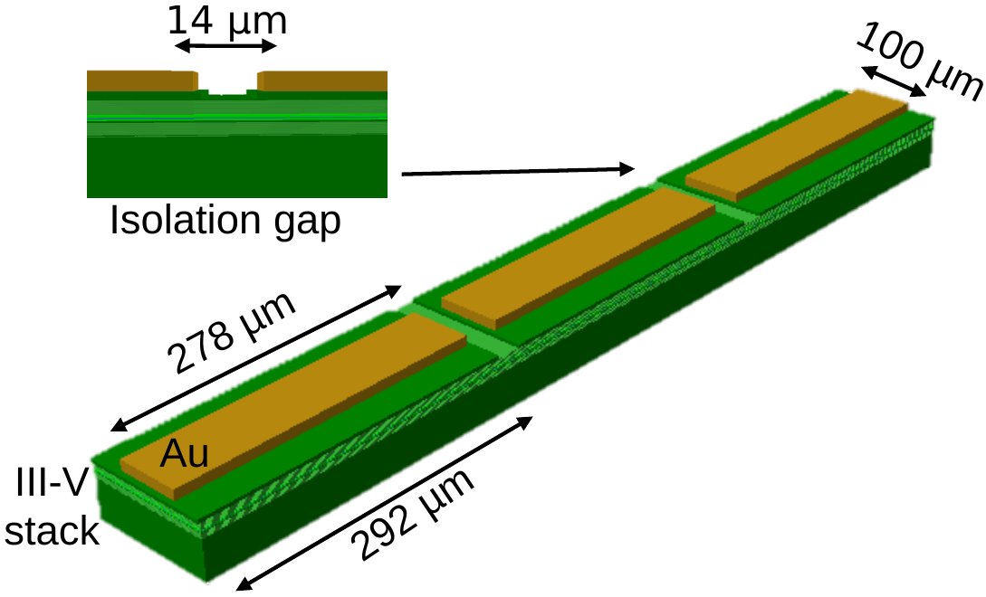
The was measured using the segmented contact method [23] using the structure shown in Fig. 1. Two identical structures were fabricated with the stacks shown in Table 1. The top gold () contacts have dimensions , and the separation between them is . The top layer in the stack is doped over to guarantee Ohmic contacts with . Gaps of in length and in depth were etched in the top layers to isolate the contacts electrically. During the measurement, the leakage current was compensated as the resistance between contacts and the leakage current change with temperature from to .
The measurements of the are shown in Fig. 2(a) for the stack with doped barriers and Fig. 2(b) for the stack with barriers. Both figures show the change in absorption for a reverse bias voltage swing of and the absorption at a reverse bias of for , , , and . The pre-biased value of is used to mitigate the modulator’s capacitance penalty as in [9].
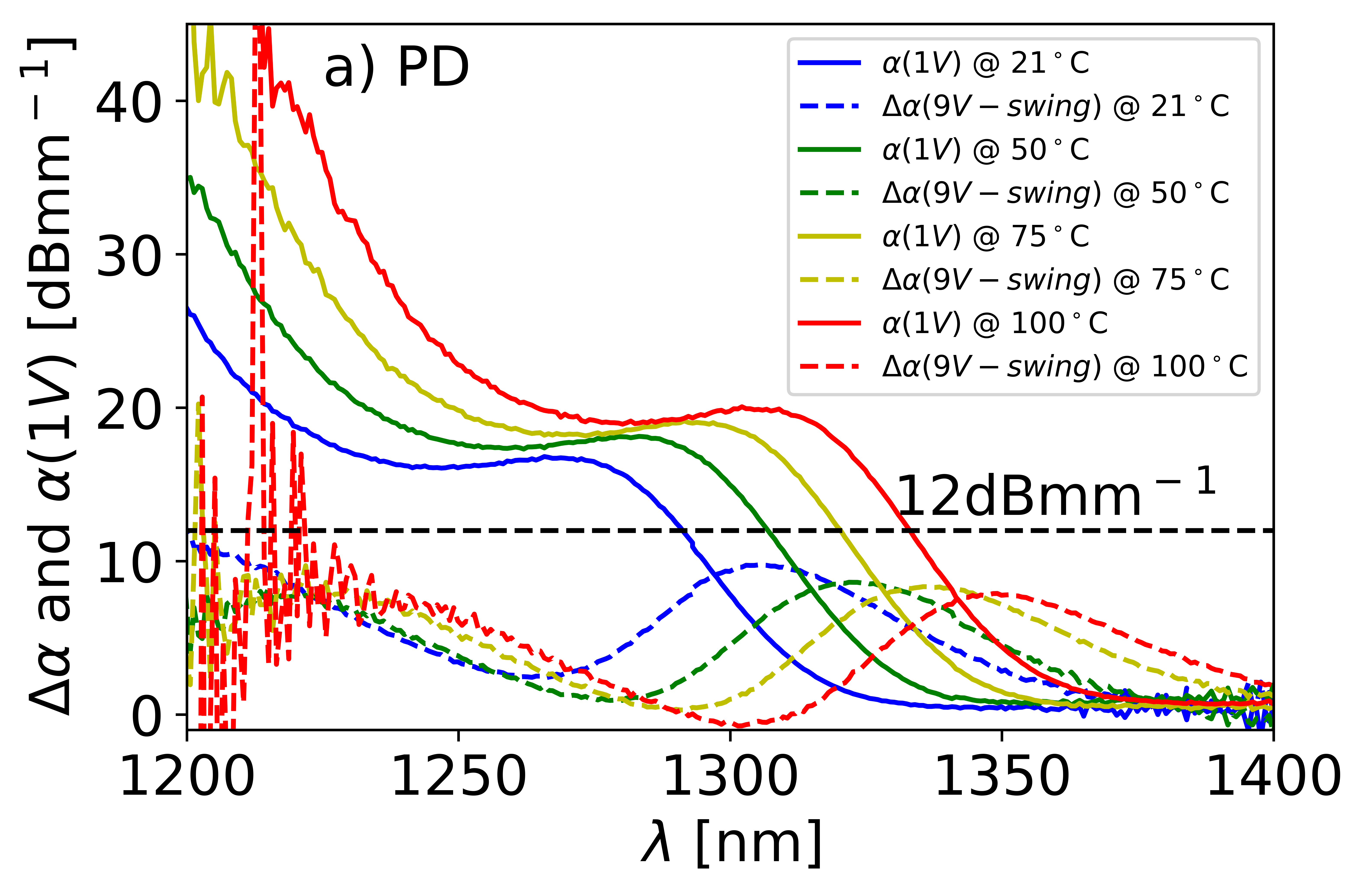
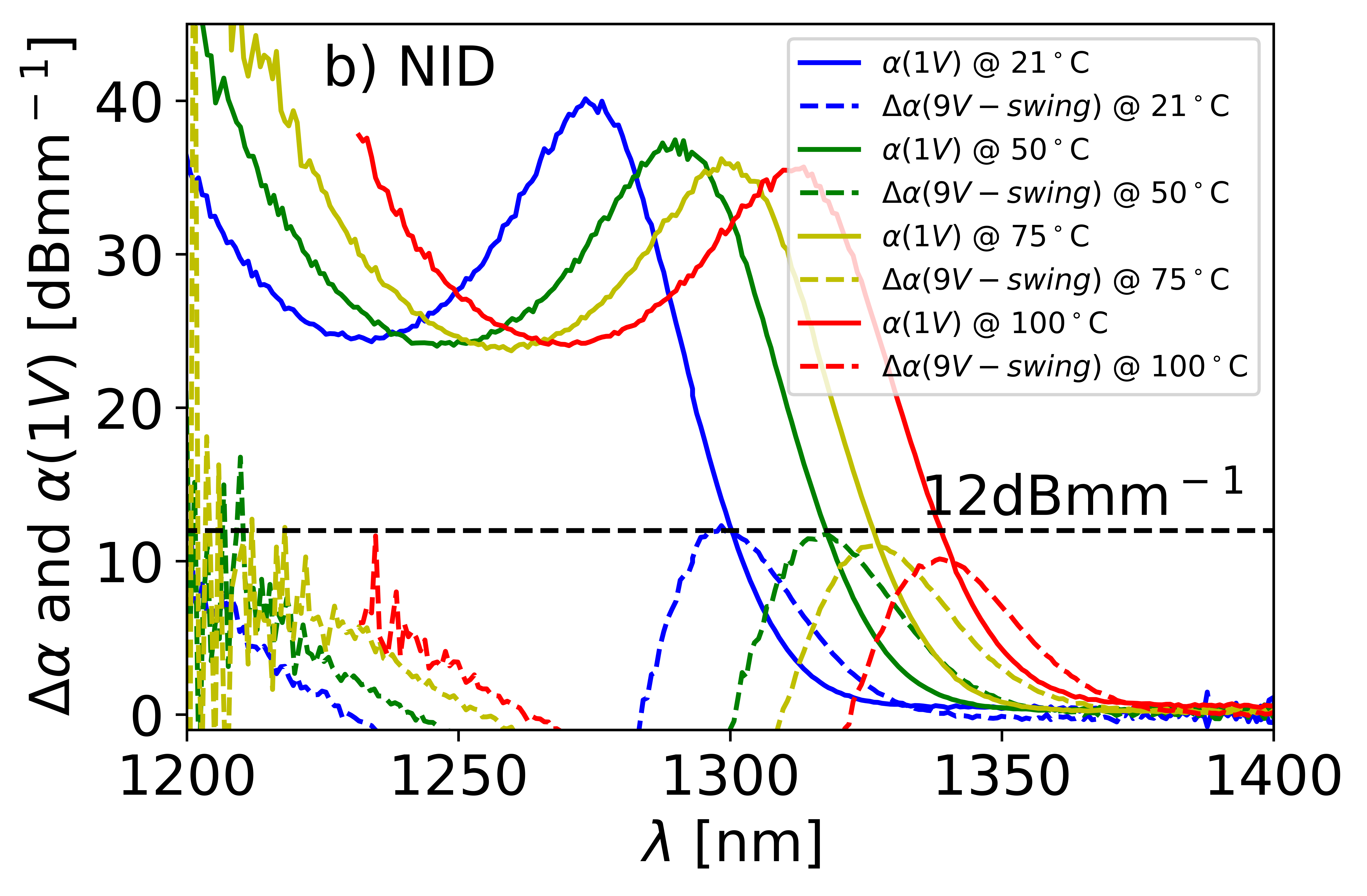
When comparing the of both stacks in Fig. 2(a) and (b), there is a slight decrease in with temperature. This will lead to a modulator with a stable from to for both stacks. Additionally, the stack with barriers has the largest value of around , which will lead to a larger . Nevertheless, it also has a larger material absorption , which will lead to a larger insertion loss ().
Regarding shown in Fig. 2(a), the stack with barrier doping does not exhibit an absorption peak at the ground-state wavelength. The ground-state absorption peak suppression is attributed to the injection of holes in the valence ground-state from the p-doped barrier. The holes inhibit the excitation of electrons from the valence ground-state to the conduction ground-state and inhibit photon absorption. Furthermore, the doping in the barriers will contribute to increasing the absorption. Nevertheless, the contribution is minimal due to the small area of the barriers compared to the entire active region. On the other hand, the stack with barriers has the expected ground-state absorption peak, as shown in Fig. 2(b).
Additionally, the maximum absorption around of the stack with doped barriers increases slightly with increasing temperature, as shown in Fig. 2(a). This behavior is attributed to the redistribution of carriers in the valence ground-states as the temperature increases. The redistribution leads to a greater occupancy probability for electrons in the top valence states, which increases photon absorption. On the other hand, the ground-state absorption peak of the stack with barriers in Fig. 2(b) decreases with increasing temperature as expected from the in . The same trend was measured in [24].
To investigate the trends further, the ground-state absorption peak for the stack with p-doped () and barriers as a function of reverse bias was measured in Fig. 3(a) for three temperatures , , and . Additionally, the absorption peak wavelength shift is represented in Fig. 3(b). The ground-state absorption peak wavelength is the wavelength that has the ground-state absorption peak.
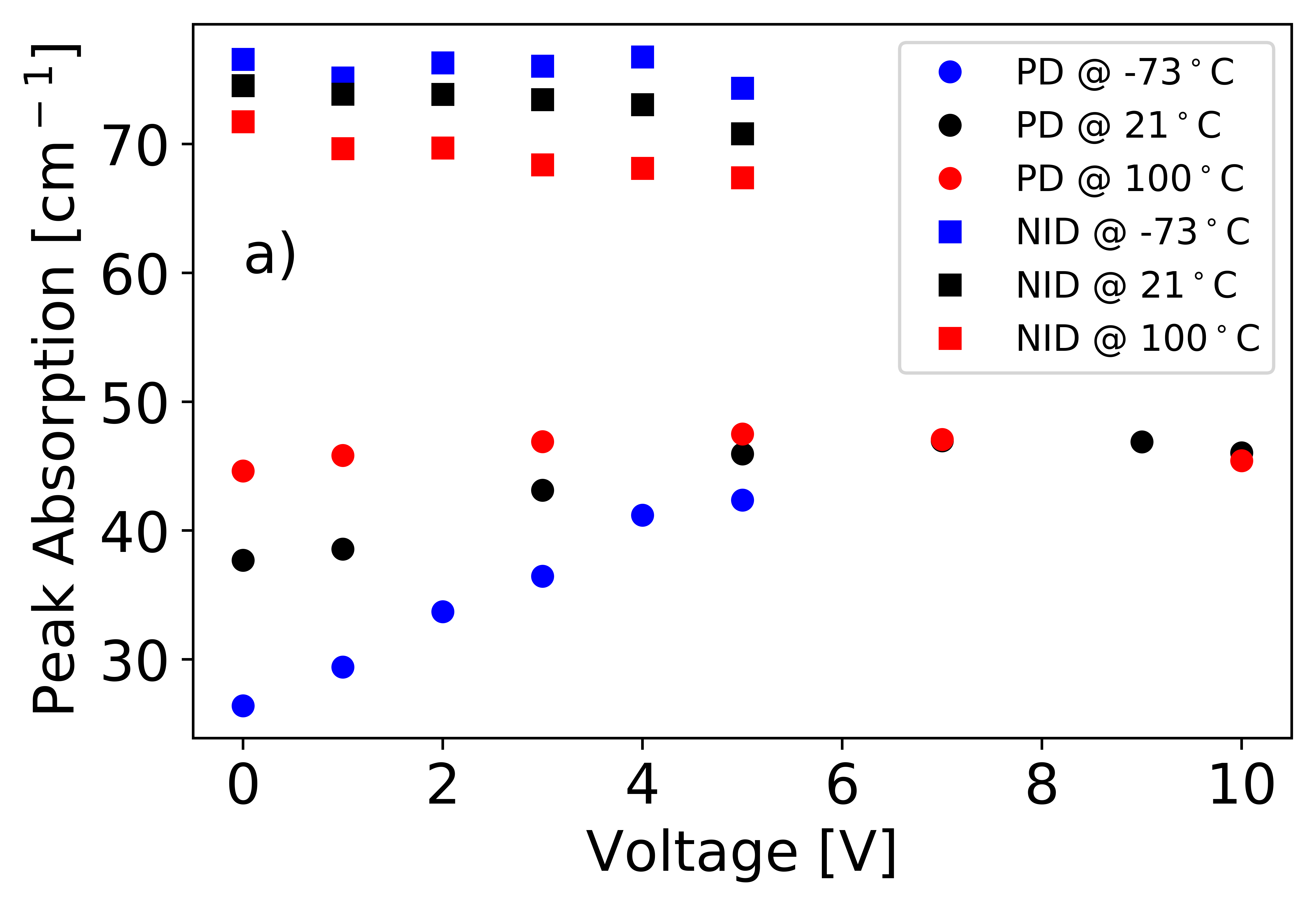
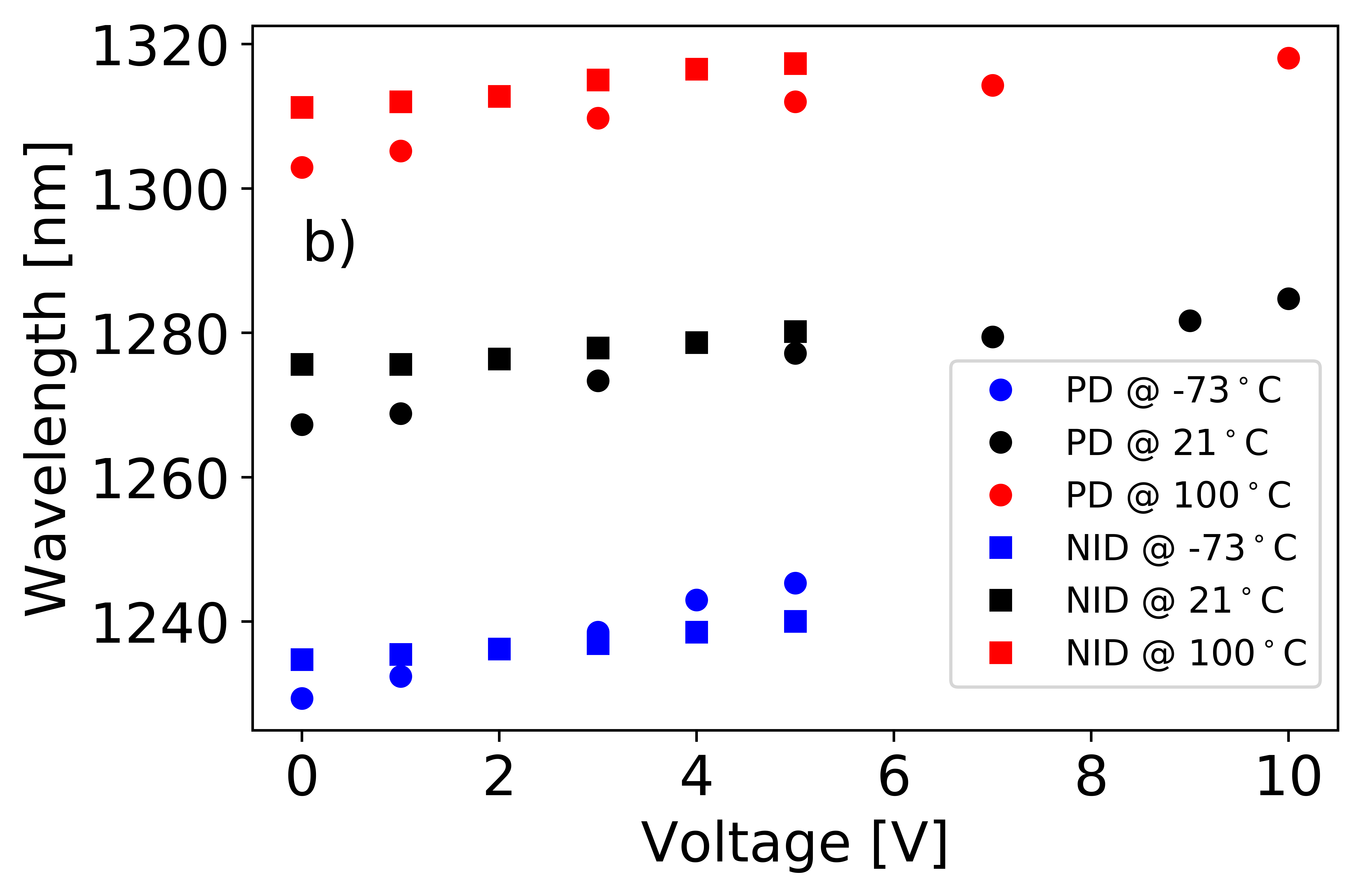
As shown in Fig. 3(a), the stack with barriers has a constant reduction in the ground-state absorption peak with increasing reverse bias at , , and . As the reverse bias increases, the increased static electric field pulls the electrons and holes in opposite directions inside the . This phenomenon leads to a reduction in the overlap between the carriers’ wavefunctions and contributes to reducing the photon absorption [25].
On the other hand, the stack with p-doped barriers has different behavior. Below moderate reverse bias (< ), the holes at the valence state’s top inhibit the photon absorption. As the reverse bias increases, the built-in static electric field depletes the holes from the top valence state, allowing photons to excite electrons from the valence ground-state to the bottom of the conduction ground-state. For voltages below , the ground-state absorption peak is smaller at rather than at due to more electrons being thermally excited to the top of the valence ground-state at higher temperatures. For the same reason, the gradient of the ground-state absorption peak at is more significant between and .
The ground-state absorption peak will increase with a reverse bias for all temperatures until all holes are entirely depleted from the top of the valence ground-state. As shown in Fig. 3(a), all holes are depleted around , and the absorption peak starts to decrease beyond for the same reason as the stack with barriers. The built-in static electric field pulls the carriers in opposite directions reducing the carrier’s wavefunction overlap and the photon absorption.
The wavelength shift of the ground-state absorption peak is shown in Fig. 3(b). The stack with doped barriers shows a more significant shift than the stack with barriers. For reverse biases between and , red-shifts at are for the stack with doped barriers and for the stack with barriers. The shift difference is more considerable at , and it decreases with increasing temperature.
Both stacks show the Stark shift present in the . Nevertheless, the stack with doped barriers has additional contributions to the red-shift. One comes from the layers having a larger static electric field strength when compared with the stack with barriers. The larger static electric field is due to the layers being surrounded by doped layers. The static electric field distribution across the active region for both stacks is shown in Fig. 4 and it was calculated using nextnano [26].
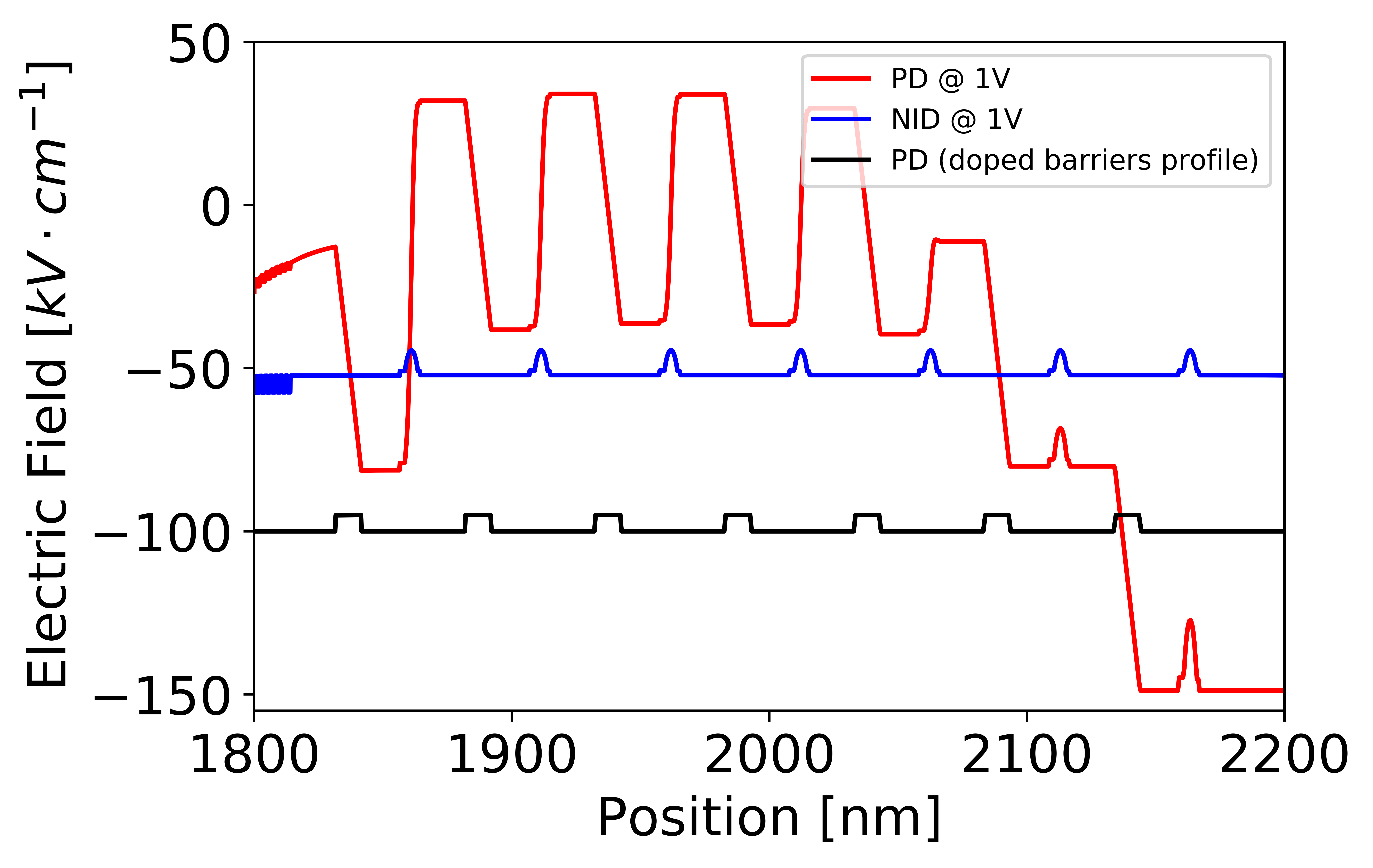
The black line at the bottom of the figure indicates the position of the doped barriers. Figure 4 highlights the significantly stronger field across the of the stack with doped barriers. Therefore, the larger static electric field would cause a more substantial red-shift.
The other shift contribution originates from the removal of holes from the highest valence states as the static electric field increases with reverse bias. As holes are depleted from the top of the valence states, longer wavelength (lower energy) transitions are allowed.
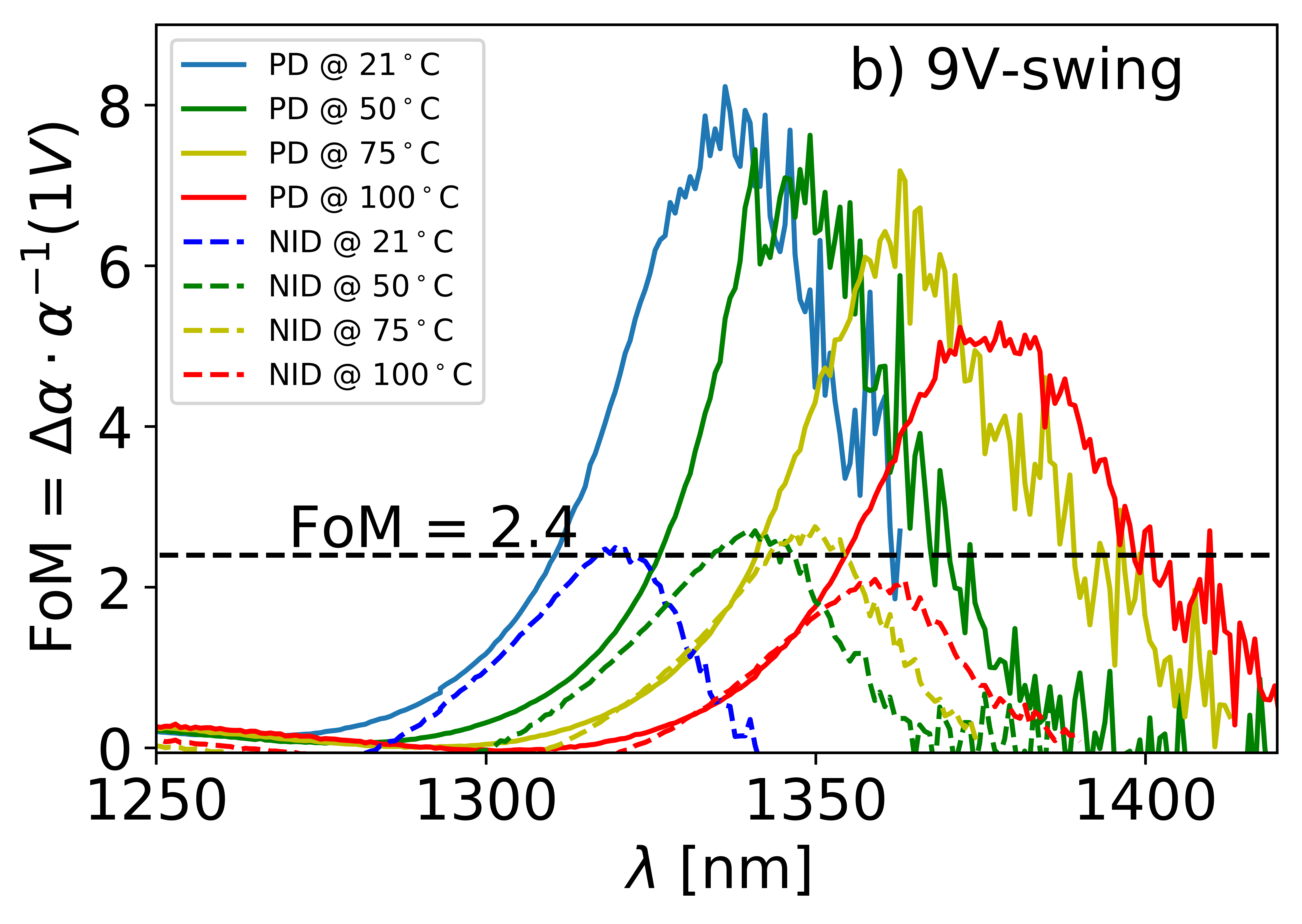
In order to determine which stack design is better for modulation, the stacks were compared using the /. The maximizes to have a large and minimizes to reduce the . The is shown in Fig. 5(a) for a -swing and in Fig. 5(b) for a -swing. A maximum swing of was used to ensure working below the breakdown static electric field of the materials. As shown in Fig. 5, the stack with p-doped barriers outperforms the stack with barriers offering up to enhancement in the from to .
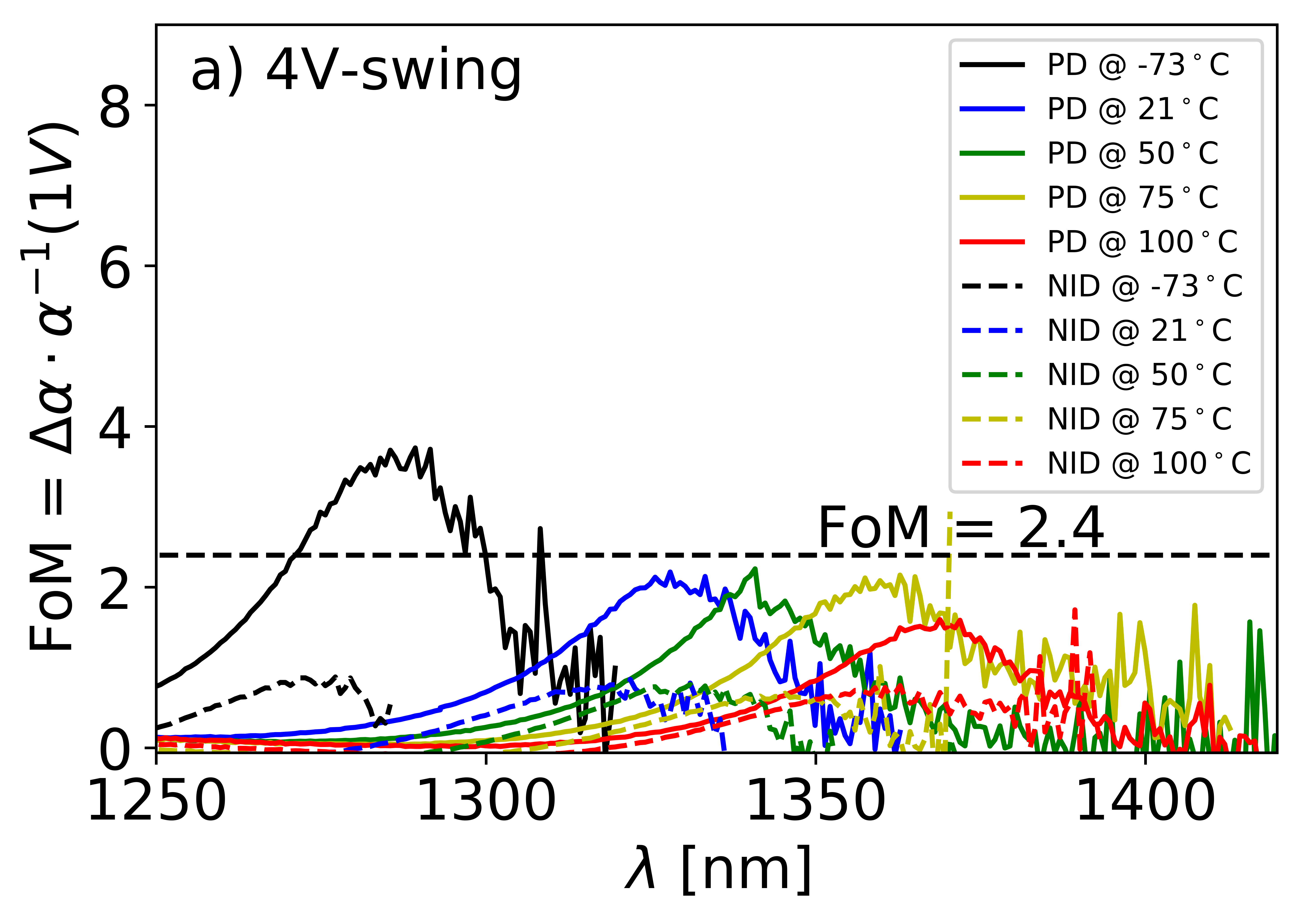
Several factors explain the better performance of the stack with doped barriers. As shown in Fig. 2, the of the stack with barriers is around , and it is slightly larger than the stack with doped barriers. Nevertheless, the ) is more significant in the stack with barriers. In this comparison, we only considered the material absorption contribution to the since both stacks will have a similar loss due to wall roughness in the modulator’s waveguide.
Additionally, the extra red-shift in the stack with doped barriers shifts away the maximum from the absorbing edge of the absorption spectrum ) represented in Fig. 2(a) offering a better trade-off /. Overall, the is better for the stack with doped barriers when considering all factors.
To explain the results in Fig. 5(a) further, the of the stack with barriers is below from to for a -swing. On the other hand, the of the stack with doped barriers is at and it is around from to . Consequently, for a -swing the of the stack with doped barriers is times larger than the stack with barriers.
Considering the results for a -swing shown in Fig. 5(b), the maximum of the stack with barriers is around from to . On the other hand, the maximum for the stack with doped barriers starts at at and degrades to at . Consequently, the of the stack with doped barriers is at least (at ) times larger than the stack with barriers. Finally, the of the stack with barriers at -swing is the same as the stack with doped barriers with a -swing. This result implies that a modulator using the stack with doped barriers may need less driving voltage which would significantly reduce power consumption.
3 Comparison with the state-of-the-art
The was measured in in slightly different stacks. Using different stack configurations can lead to changes in the , which will produce modulators with various performances. All the papers measuring the in are summarized in Table 2.
Several data/telecom applications require a minimum of around . For the mentioned , the sample with barriers will have a length of about and a material absorption contribution to the around . For most applications, that results in most optical interconnects going over the power budget. On the other hand, the sample with doped barriers will require . The material absorption contribution to the will be around , which will not exceed most optical interconnects power budgets.
This comparison only considers the material loss contribution to the . To compare both design stacks, all and were calculated assuming a modulator length of to obtain an .
The work presented in [14] reported the second-largest bandwidth around but the for a -swing is significantly lower than the one presented in this work. On the other hand, the achieved in [11] and [8] are around , which is a similar value to the one presented in this paper. However, stacks have 10 ([11]) and 12 ([8]) layers. The additional layers absorb additional light due to a more overlap between the absorbing and the optical mode. Having a thicker active region will lead to a smaller electrical bandwidth.
Finally, the work presented in [9] offers similar performance to this work. Nevertheless, it requires a larger driving voltage around -swing, and the stack has a higher density around and 8 layers.
To conclude, the stack with barriers offers similar performance to the state-of-the-art shown in Table 2. Nevertheless, when the barriers are doped, the efficiency of the for modulation is boosted, offering better performance than the state-of-the-art in terms of , driving voltage, electrical power consumption, and operational temperature from to .
4 Conclusion
This work measured the in using and p-doped barriers. The measurements indicate that doping barriers lead to a at least larger than the stack with undoped barriers from to . The better performance is due to the absence of the ground-state absorption peak and an additional component to the Stark shift due to hole depletion in the valence ground-state and a larger static electric field. To conclude, doping barriers offer better performance than the state-of-the-art stacks in terms of , driving voltage, electrical power consumption, and operational temperature from to .
Funding
Engineering and Physical Sciences Research Council (2268875).
Acknowledgments
This work is part of the feasibility study project ’Measurement of Carrier-Induced Electro-Refraction and Electro-Absorption in Quantum Dots’ funded by the EPSRC Future Manufacturing Hubs, including the Compound Semiconductor Manufacturing Hub.
We acknowledge Prof. John Donegan () for fruitful discussions. We thank Dr. Alireza Samani (), Dr. Md. Ghulam Saber (), Dr. Yannick D’Mello (), and Prof. Nicolás Bouchard () for proofreading this paper.
Disclosures
The authors declare no conflicts of interest.
Data availability statement
Data underlying the results presented in this paper are not publicly available at this time but may be obtained from the authors upon reasonable request at abadian@cardiff.ac.uk or https://orcid.org/0000-0002-7355-4245.
References
- [1] J. C. Norman, D. Jung, Y. Wan, and J. E. Bowers, “Perspective: The future of quantum dot photonic integrated circuits,” \JournalTitleAPL Photonics 3, 030901 (2018).
- [2] Y. Wan, J. C. Norman, Y. Tong, M. J. Kennedy, W. He, J. Selvidge, C. Shang, M. Dumont, A. Malik, H. K. Tsang, A. C. Gossard, and J. E. Bowers, “1.3 µm quantum dot-distributed feedback lasers directly grown on (001) Si,” \JournalTitleLaser & Photonics Reviews 14, 2000037 (2020).
- [3] E. D. Le Boulbar, L. Jarvis, D. Hayes, S. Shutts, Z. Li, M. Tang, H. Liu, A. Samani, P. M. Smowton, and N. Abadía, “Temperature dependent behavior of the optical gain and electroabsorption modulation properties of an InAs/GaAs quantum dot epistructure,” in 2019 21st International Conference on Transparent Optical Networks (ICTON), (2019), p. 1–4.
- [4] T. Kageyama, K. Nishi, M. Yamaguchi, R. Mochida, Y. Maeda, K. Takemasa, Y. Tanaka, T. Yamamoto, M. Sugawara, and Y. Arakawa, “Extremely high temperature (220°c) continuous-wave operation of 1300-nm-range quantum-dot lasers,” in 2011 Conference on Lasers and Electro-Optics Europe and 12th European Quantum Electronics Conference (CLEO EUROPE/EQEC), (2011), p. 1–1.
- [5] D. A. B. Miller, “Device requirements for optical interconnects to silicon chips,” \JournalTitleProceedings of the IEEE 97, 1166–1185 (2009).
- [6] L. Vivien and L. Pavesi, Handbook of Silicon Photonics, Series in Optics and Optoelectronics (CRC Press, 2016).
- [7] N. Abadía, T. Bernadin, P. Chaisakul, S. Olivier, D. Marris-Morini, R. E. de Lamaëstre, J. C. Weeber, and L. Vivien, “Low-power consumption Franz-Keldysh effect plasmonic modulator,” \JournalTitleOpt. Express 22, 11236–11243 (2014).
- [8] C.-H. Lin, J.-P. Wu, Y.-Z. Kuo, Y.-J. Chiu, T. Tzeng, and T. Lay, “InGaAs self-assembly quantum dot for high-speed 1300 nm electroabsorption modulator,” \JournalTitleJournal of Crystal Growth 323, 473–476 (2011). Proceedings of the 16th International Conference on Molecular Beam Epitaxy (ICMBE).
- [9] S. A. Sobhani, B. J. Stevens, N. Babazadeh, K. Takemasa, K. Nishi, M. Sugawara, R. A. Hogg, and D. T. D. Childs, “Proposal for common active 1.3 μm quantum dot electroabsorption modulated DFB laser,” \JournalTitleIEEE Photonics Technology Letters 31, 419–422 (2019).
- [10] Y. Luo, B. Xiong, J. Wang, P. Cai, and C. Sun, “40 GHz AlGaInAs multiple-quantum-well integrated electroabsorption modulator/distributed feedback laser based on identical epitaxial layer scheme,” \JournalTitleJapanese Journal of Applied Physics 45, L1071–L1073 (2006).
- [11] C. Y. Ngo, S. F. Yoon, W. K. Loke, Q. Cao, D. R. Lim, V. Wong, Y. K. Sim, and S. J. Chua, “Characteristics of 1.3 μm InAs/InGaAs/GaAs quantum dot electroabsorption modulator,” \JournalTitleApplied Physics Letters 94, 143108 (2009).
- [12] M. Areiza, C.-B. Tribuzy, S. Landi, M. Pires, and P. Souza, “Amplitude modulators containing an nipi delta doping superlattice,” \JournalTitleIEEE Photonics Technology Letters 17, 2071–2073 (2005).
- [13] I. Sandall, J. Ng, J. David, H. Liu, and C. Tan, “Evaluation of InAs quantum dots on Si as optical modulator,” \JournalTitleSemiconductor Science and Technology 28, 094002 (2013).
- [14] Y. Chu, M. Thompson, R. Penty, I. White, and A. Kovsh, “1.3 μm quantum-dot electro-absorption modulator,” in Conference on Lasers and Electro-Optics/Quantum Electronics and Laser Science Conference and Photonic Applications Systems Technologies, (Optical Society of America, 2007), p. CMP4.
- [15] Y. Tang, J. D. Peters, and J. E. Bowers, “Over 67 GHz bandwidth hybrid silicon electroabsorption modulator with asymmetric segmented electrode for 1.3 μm transmission,” \JournalTitleOpt. Express 20, 11529–11535 (2012).
- [16] P. Chaisakul, M.-S. Rouifed, D. Marris-Morini, G. Isella, D. Chrastina, J. Frigerio, X. Le Roux, S. Edmond, J.-R. Coudevylle, and L. Vivien, “High speed electro-absorption modulator based on quantum-confined Stark effect from Ge/SiGe multiple quantum wells,” in The 9th International Conference on Group IV Photonics (GFP), (2012), p. 60–62.
- [17] E. H. Edwards, L. Lever, E. T. Fei, T. I. Kamins, Z. Ikonic, J. S. Harris, R. W. Kelsall, and D. A. B. Miller, “Low-voltage broad-band electroabsorption from thin Ge/SiGe quantum wells epitaxially grown on silicon,” \JournalTitleOpt. Express 21, 867–876 (2013).
- [18] D. T. Neilson, L. C. Wilkinson, D. J. Goodwill, A. C. Walker, B. Vögele, M. McElhinney, F. Pottier, and C. R. Stanley, “Effects of lattice mismatch due to partially relaxed buffer layers in InGaAs/AlGaAs strain balanced quantum well modulators,” \JournalTitleApplied Physics Letters 70, 2031–2033 (1997).
- [19] D. A. B. Miller, “Energy consumption in optical modulators for interconnects,” \JournalTitleOpt. Express 20, A293–A308 (2012).
- [20] Z. Zhang, D. Jung, J. C. Norman, P. Patel, W. W. Chow, and J. E. Bowers, “Effects of modulation p doping in InAs quantum dot lasers on silicon,” \JournalTitleApplied Physics Letters 113, 061105 (2018).
- [21] N.-N. Feng, D. Feng, S. Liao, X. Wang, P. Dong, H. Liang, C.-C. Kung, W. Qian, J. Fong, R. Shafiiha, Y. Luo, J. Cunningham, A. V. Krishnamoorthy, and M. Asghari, “30 GHz Ge electro-absorption modulator integrated with 3 μm silicon-on-insulator waveguide,” \JournalTitleOpt. Express 19, 7062–7067 (2011).
- [22] S. A. Srinivasan, C. Porret, E. Vissers, P. Favia, J. De Coster, H. Bender, R. Loo, D. Van Thourhout, J. Van Campenhout, and M. Pantouvaki, “High absorption contrast quantum confined Stark effect in ultra-thin Ge/SiGe quantum well stacks grown on Si,” \JournalTitleIEEE Journal of Quantum Electronics 56, 1–7 (2020).
- [23] J. Mahoney, P. M. Smowton, B. Maglio, L. Jarvis, C. Allford, S. Shutts, M. Tang, H. Liu, and N. Abadía, “QCSE and carrier blocking in p-modulation doped InAs/InGaAs quantum dots,” in Conference on Lasers and Electro-Optics, (Optical Society of America, 2021), p. JTu3A.167.
- [24] C. Cornet, C. Labbé, H. Folliot, N. Bertru, O. Dehaese, J. Even, A. Le Corre, C. Paranthoen, C. Platz, and S. Loualiche, “Quantitative investigations of optical absorption in InAs∕InP(311)B quantum dots emitting at 1.55 μm wavelength,” \JournalTitleApplied Physics Letters 85, 5685–5687 (2004).
- [25] P. W. Fry, I. E. Itskevich, D. J. Mowbray, M. S. Skolnick, J. J. Finley, J. A. Barker, E. P. O’Reilly, L. R. Wilson, I. A. Larkin, P. A. Maksym, M. Hopkinson, M. Al-Khafaji, J. P. R. David, A. G. Cullis, G. Hill, and J. C. Clark, “Inverted electron-hole alignment in InAs-GaAs self-assembled quantum dots,” \JournalTitlePhys. Rev. Lett. 84, 733–736 (2000).
- [26] S. Birner, “nextnano: General purpose 3-D simulations,” \JournalTitleIEEE Transactions on Electron Devices 54, 2137–2142 (2007).