suppl
Synthesis and electronic properties of Ndn+1NinO3n+1 Ruddlesden-Popper nickelate thin films
Abstract
The rare-earth nickelates possess a diverse set of collective phenomena including metal-to-insulator transitions, magnetic phase transitions, and, upon chemical reduction, superconductivity. Here, we demonstrate epitaxial stabilization of layered nickelates in the Ruddlesden-Popper form, Ndn+1NinO3n+1, using molecular beam epitaxy. By optimizing the stoichiometry of the parent perovskite NdNiO3, we can reproducibly synthesize the member compounds. X-ray absorption spectroscopy at the O and Ni edges indicate systematic changes in both the nickel-oxygen hybridization level and nominal nickel filling from 3 to 3 as we move across the series from to . The compounds exhibit weakly hysteretic metal-to-insulator transitions with transition temperatures that depress with increasing order toward NdNiO3 (.
I Introduction
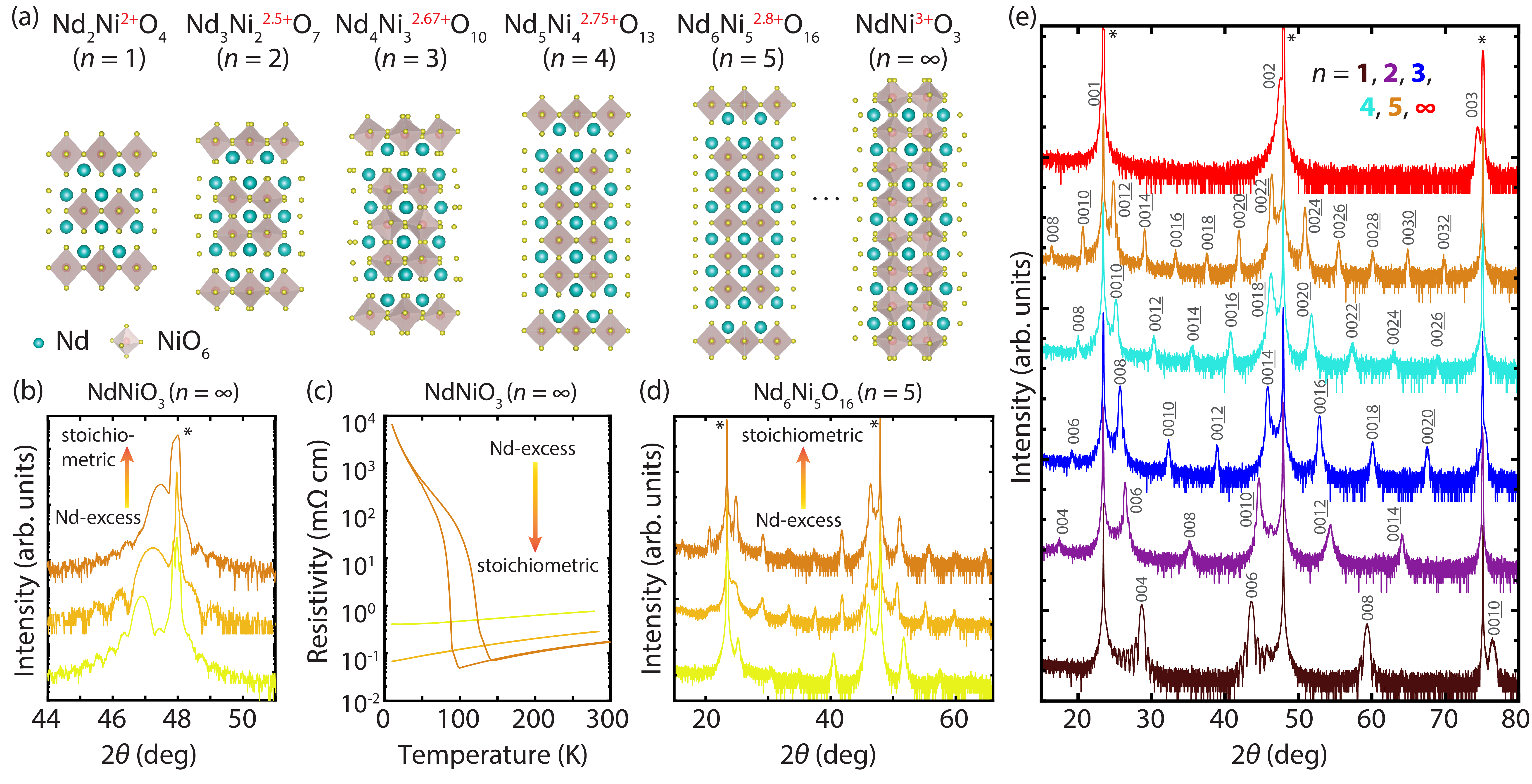
The perovskite rare earth nickelates NiO3 ( = La, Pr, Nd…) are strongly correlated materials with a rich, tunable phase diagram that includes features such as metal-to-insulator transitions and non-collinear antiferromagnetism [1, 2]. The Ruddlesden-Popper nickelates, represented by the chemical formula NinO3n+1, are the layered analogues of the perovskite rare-earth nickelates. Also expressed as (NiO3)n(O), these compounds comprise layers of the traditional perovskite motif NiO3 separated by rock salt spacer layers -O as shown in Fig. 1(a). The -O layer tunes the dimensionality of the system from the three-dimensional NiO3 () to the quasi two-dimensional NiO4 ( = 1). The phenomenology of the NiO4 family of compounds is distinct from its perovskite counterparts: for example, while the perovskite LaNiO3 is a strongly correlated metal [1, 3, 4], single-layer La2NiO4 displays insulating charge and spin stripes, with a spatial modulation tunable with doping [5, 6]. Accordingly, the evolution of the charge and spin structure with perovskite layer thickness (or ‘order’) in the Ruddlesden-Popper nickelates has been of sustained interest, especially as many of these ordered phases precede superconductivity in the cuprates [7]. Indeed, the Ruddlesden-Popper nickelates have long been viewed as close cousins of the cuprates [8, 9, 10] and it was recently found that the compounds exhibit superconductivity when chemically reduced into the square-planar form [11, 12].
Despite longstanding interest, synthesis of the Ruddlesden-Popper nickelates remains a key challenge. Early studies on the member compounds in powder form identified analogies to the superconducting cuprates including a putatively similar band structure and possible charge density wave transitions [13, 14, 8, 15]. More recently, advances in the preparation of large single-crystal specimens [10, 16] have enabled direct study of these features which were originally proposed from powder specimen behavior [17, 18]. Nevertheless, the higher-order compounds (), which are of particular interest as the becomes superconducting when reduced [12], remain inaccessible using powder or single crystal synthetic methods [16]. Instead, these compounds require atomic layering control. In addition to the synthesis of the superconducting square-planar compound with molecular beam epitaxy (MBE), the stabilization of the Lan+1NinO3n+1[19] and Ndn+1NinO3n+1[20] series for also using MBE has recently been reported. Atomically-precise thin film deposition thus allows access to the NinO3n+1 series beyond .
In this paper, we describe a generalizable synthetic strategy for thin film Ruddlesden-Popper nickelates Ndn+1NinO3n+1 ( = 1 – 5), using MBE. By first optimizing the crystalline growth of the perovskite NdNiO3 on LaAlO3 substrates, we can reproducibly stabilize the higher-order layered Ruddlesden-Popper nickelates. From x-ray absorption spectra (XAS), we observe that tuning the layering of the Ruddlesden-Popper nickelates changes the nickel electronic filling and relative transition-metal-oxygen hybridization levels, as would be expected from electron counting rules. Furthermore, there are systematic changes in the x-ray linear dichroism (XLD) which we attribute to energy level splittings in the orbitals. In the electronic transport, we observe in the compounds metal-to-insulator transitions with features that interpolate between those of the parent perovskite NdNiO3 and bulk crystal specimens of Ndn+1NinO3n+1 ( = 3) [8].
II Experimental Methods
II.1 Synthesis via MBE
We use ozone-assisted MBE to synthesize the Ruddlesden-Popper nickelates in the thin film form. The evolution of the nickel valence from Ni2+ in the Nd2NiO4 () compound to Ni3+ in the NdNiO3 compound necessitates varied synthetic conditions [16]—as hot as 1000°C for Nd2NiO4 and as cold as 550°C for NdNiO3. We synthesize the Nd2NiO4 () compound using the simultaneous evaporation of both elements (hereafter, ‘codeposition’) at high (900-1000 °C) temperatures with fluxes estimated using a quartz crystal microbalance with applied tooling factors. We also note that it is possible to synthesize the = 2, 3 and perovskite layer compounds using the codeposition method by tuning only the relative flux ratios, temperature and oxidation pressure, similar to what has been done for single crystals [16]. On the other hand, the compounds, which have not been synthesized as bulk crystals, also cannot be synthesized with codeposition. These compounds therefore require the precise sequential deposition of the neodymium and nickel sources, wherein a single monolayer of each element is deposited at a time, to achieve the Ruddlesden-Popper layering.
In principle, MBE enables one to precisely control the monolayer deposition times and hence synthesize a generic Ruddlesden-Popper compound of arbitrary order . There are key differences however between the Ruddlesden-Popper nickelates and other Ruddlesden-Popper systems such as the more commonly studied Srn+1TinO3n+1 which make the direct translation of other synthetic calibration techniques onto the nickelates difficult. In Srn+1TinO3n+1 compounds, deviations from perfect stoichiometry by as much as 5+% often result in imperfect superlattices with rock salt intergrowths or missing rock salt layers but without substantial phase segregation [21, 22]. Errors in monolayer dosing times can then be quantitatively estimated and adjusted for purely based on x-ray diffraction spectra of the superlattice phase [23]. The composition, or : cation ratio in an O3 compound, can also be perfected using quantitative analysis of the beat frequencies and oscillation lineshapes in the reflection high energy electron diffraction (RHEED) intensities [24, 22].
In contrast, a principal challenge in nickelate thin film synthesis is the stabilization of the high oxidation Ni3+ state. Insufficient oxidizing conditions can promote the phase segregation of Ni2+ compounds such as polycrystalline NiO [9, 25]. The presence of NiO however, can result not only from insufficient oxidation, but also from errors in composition or monolayer dosing, and most frequently from a combination of all three. This propensity to phase segregate makes assessing quantitative changes to monolayer dosing challenging. Moreover, it is difficult to use RHEED oscillations to precisely adjust for composition errors: once a secondary phase such as NiO forms, RHEED oscillation intensities fade and do not recover, whereas oscillations can persist for much longer in SrTiO3-based compounds [24, 22].
To address these challenges we have developed an alternative calibration method that reliably facilitates the synthesis of Ruddlesden-Popper Ndn+1NinO3n+1 compounds. This method optimizes the synthesis of the parent perovskite NdNiO3: by iteratively improving both its stoichiometric composition and monolayer dose estimates, we can obtain precise shuttering times to synthesize the higher order Ruddlesden-Popper compounds with atomistic precision. We start by adjusting the temperature of the neodymium and nickel effusion cells to read atoms cm-1s-1 on a quartz crystal microbalance. We then synthesize the binary oxides Nd2O3 on Y:ZrO2 (111) and NiO on MgO (100) and use x-ray reflectivity (XRR) to estimate the film thicknesses and thus the actual effusion cell fluxes [26]. These estimates give us approximate values of the neodymium and nickel fluxes, which we then fine tune with the synthesis of NdNiO3.
From the rough flux estimates provided by the binary oxide compounds, we perform the shuttered growth of NdNiO3. In our initial calibration scheme, we intentionally deposit less than one full monolayer of both neodymium and nickel. The accidental deposition of more than one full monolayer can exacerbate the formation of polycrystalline NiO phases, which would be observed in the RHEED (Fig. S4 of the Supplemental Material [27]), even if the elements are supplied in a one-to-one composition ratio. Hence in this “underdosed” regime, we can focus on tuning the composition ratio of neodymium and nickel. Similar to other oxide perovskites [22], the parent compound NdNiO3 is capable of accommodating some -site (neodymium) excess into the lattice, while still forming a single-phase film, as ascertained by RHEED and atomic force microscopy (AFM). This -site excess is manifest as an expansion of the out-of-plane lattice constant as well as in a broadening or even suppression of the metal-to-insulator transition [28, 29]. By tracking the evolution of the lattice constants for a range of Nd:Ni ratios, we have found that an optimally stoichiometric NdNiO3 film on LaAlO3 possesses a lattice constant of 3.82 Å corresponding to a (002) film peak that nearly coincides with that of the substrate LaAlO3 [28, 29]. The metal-to-insulator transition in these stoichiometric films spans as much as over five orders of magnitude; films with excess neodymium have a higher room temperature resistivity and may possess a entirely suppressed metal-to-insulator transition. We note that it is also possible to form a nickel-rich NdNiO3 phase [25], though we have found that nickel excess will more frequently appear as a secondary NiO phase in situ in the RHEED pattern (Fig. S4 in the Supplemental Material [27]). After fine-tuning this shuttered stoichiometric calibration in the underdosed regime, we then correct for the monolayer dosing using thickness estimates from XRR fits to the NdNiO3 films. Finally, we apply the monolayer deposition times from the calibrated NdNiO3 to synthesize the Ruddlesden-Popper compounds. We synthesize the Ndn+1NinO3n+1 () compounds at a substrate temperature of 630 – 690°C as verified by an optical pyrometer and using distilled ozone in chamber pressures of 1.2 – 2.0 Torr.
Figures 1(b)-1(d) illustrates this approach using three different calibrations from NdNiO3 films. The stoichiometric film possesses a lattice constant of 3.82(7) Å; in contrast, the -site-rich films have expanded lattice constants of 3.84(5) and 3.87(3) Å, corresponding to neodymium in excess of 3% and 10%, respectively, estimated from our neodymium flux calibrations (Fig. 1(b)). Importantly, we note that this -site excess is not always manifest in surface-sensitive characterization such as RHEED or AFM (Fig. S4 in the Supplemental Material [27]) images, which show that the -site excess films are ostensibly high quality. Hence, we confirm the superior quality of the stoichiometric film using resistivity measurements which present a sharp metal-to-insulator transition in Fig. 1(c). Finally, using the three different shuttered calibrations from these three NdNiO3 films, we synthesize the Nd6Ni5O16 ( = 5) compound. As shown in the XRD spectra in Fig. 1(d), the Nd6Ni5O16 synthesized from the two -site excess films display predominant Ruddlesden-Popper layering but with weaker superlattice ordering. The Nd6Ni5O16 film synthesized from the least stoichiometric NdNiO3 calibration possesses superlattice peaks approaching those of an compound, and neither film exhibits sharp lower order peaks. In contrast, the Nd6Ni5O16 film synthesized from the stoichiometric NdNiO3 calibration displays coherent ordering with the full emergence of the lower order (0010) and (0012) superlattice peaks, which are sensitive to the long-range order of the film. This indicates the sensitivity of the Ruddlesden-Popper nickelates to composition, requiring a calibration procedure that enables fine tuning.
II.2 Structural characterization
Thin film XRD spectra were taken on Malvern Panalytical Empyrean diffractometer using Cu K ( Å) radiation. Reciprocal space maps (RSMs) were taken on the same instrument using a PIXcel3D 2D pixel area detector. Cross-section scanning transmission electron microscopy (STEM) specimens were prepared using an FEI Helios focused-ion beam with a gallium ion source. The final thinning step was performed using 2 keV gallium ions. Atomic-resolution STEM imaging was performed using a Thermo Fisher Scientific Themis Z G3 transmission electron microscope operated at 200 keV with probe convergence angle of 19.6 mrad and an annular dark-field (ADF) collection angle range of 78–200 mrad. Additional STEM imaging was performed on an aberration-corrected JEOL ARM 200F transmission electron microscope at 200 keV with a probe convergence angle of 22 mrad and an ADF collection angle range of 68–220 mrad. The displayed images were obtained from the average of 20 cross-correlated frames each acquired with 500 nS dwell time.
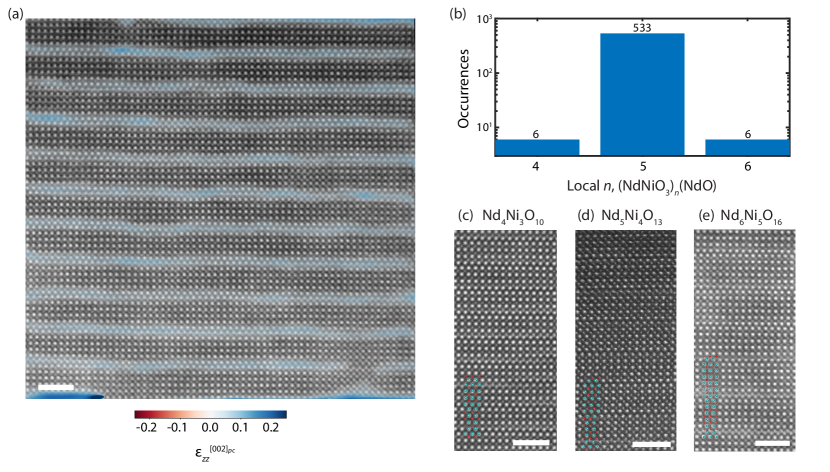
To map the local distortions of specific lattice fringes, we performed a phase lock-in analysis on the high-angle ADF STEM (HAADF-STEM) images. By taking the gradient of the local phase, we can generate a map of local strain along the direction [30, 31, 32]. The strain map highlights Ruddlesden-Popper rock salt layers, which appear as regions of local tensile strain beacuse the spacing between two adjacent Nd-O layers (2.7 Å) is greater than the spacing between the adjacent Nd-O and Ni-O layers (1.9 Å). Analyzing the strain profiles along the -direction can thus be used to quantify distances between the rock salt space layers. This allows us to determine the locations and occurrences of local layerings within a film, as demonstrated in Fig. 2. Further details on the phase lock-in analysis may be found in the Supplemental Material [27].
| Order | Hypothetical valence (filling) | Measured valence | -axis lattice constant (Å) | Unit-cell volume (Å3) |
|---|---|---|---|---|
| = 1 | 2+ () | 2+ (nominal) | 12.450 0.002 | 361 0.06 |
| = 2 | 2.5+ () | 2.5(7)+ | 20.20 0.05 | 580 1.5 |
| = 3 | 2.67+ () | 2.6(7)+ | 27.728 0.015 | 797 0.43 |
| = 4 | 2.75+ () | 2.7(9)+ | 35.35 0.07 | 1016 2 |
| = 5 | 2.8+ () | 2.8(4)+ | 43.12 0.04 | 1239 1.2 |
II.3 X-ray absorption spectroscopy
XAS were measured at the Advanced Light Source, Lawrence Berkeley National Lab, at Beamlines 4.0.2 and 6.3.1 in the total electron yield mode at 300 K. At Beamline 4.0.2 the spectra were acquired at 20° grazing incidence with linear horizontally () or vertically () polarized photons. At Beamline 6.3.1, the spectra were acquired exclusively with linear horizontally polarized incident photons but with the sample either normal () or at 30° grazing () to the beam. A geometric correction factor was applied for the grazing incident signal [33]. As energy calibrations can differ slightly between beamline endstations, we use Nd features to align all Ni - and O -edge spectra. All spectra are normalized to the incident x-ray flux, as monitored via the absorption by a semitransparent gold mesh upstream of the nickelate films. The spectra are further scaled so that the intensity is unity at energies slightly below the absorption edge, and normalized across the entire edge. Each spectrum presented is polarization-averaged [] and represents the mean of 8-16 polarization-averaged scans. All x-ray linear dichroism (XLD) signals are given by (), the difference between spectra with photons polarized predominantly out-of-plane and in-plane with respect to the sample surface. The XLD spectra are normalized by the polarization-averaged integral [34].
II.4 Electrical transport
Electrical resistivities were determined using devices in van der Pauw or Hall bar geometries. Contacts comprising Cr (5 nm)/Au (100 nm) were deposited using an electron-beam evaporator and patterned with shadow masks. Hall bar channels were defined with a diamond scribe. Transport measurements down to 1.8 K were conducted in a Quantum Design Physical Property Measurement System equipped with a 9 T magnet using AC lock-in techniques at 15 Hz. Temperature-dependent Hall coefficients were calculated from linear fits of anti-symmetrized field sweeps up to 9 T, all taken upon warming.
III Results and Discussion
III.1 Thin film growth
Using the growth calibration techniques described above, we present the XRD spectra of the fully epitaxially stabilized nickelate Ruddlesden-Poppers ( 1 – 5) on LaAlO3 in Fig. 1(e). The XRD spectra display all the allowed even-numbered (00) superlattice peaks. We extract the out-of-plane lattice constants from Nelson-Riley fits to the 2- spectra [35], tabulated in table 1.
To determine the in-plane lattice constants, we perform RSMs on each of the films (see Fig. S2 in the Supplemental Material [27]). RSM scans indicate that the films are epitaxially strained to the LaAlO3 substrate ( Å), which provides strain to the bulk NdNiO3 () and as much as strain to the bulk Nd4Ni3O10 (). However, our single-layer Nd2NiO4 () film, which experiences a similar strain level of , appears to have partially relaxed to an average Å. This is still under the bulk lattice constant of Å. This relaxation is likely order-dependent; for example, in the single-layer Ruddlesden-Popper ruthenate Sr2RuO4, immediate relaxation has been reported on substrates providing strain [36]. Indeed, while our Nd2NiO4 () film exhibits partial relaxation as early as 17 nm, we could stabilize the Nd4Ni3O10 () to around 55 nm before we observed partial relaxation (see Fig. S3 of the Supplemental Material [27]). The films presented in Fig. 1(e) were all synthesized to have 60–75 nickel layers, resulting in thicknesses of 29.5, 27.7, 26.5, 32.4, and 22.9 nm for the compounds, respectively; meanwhile, the compound presented is 17 nm thick. With these in-plane lattice constants, we report the unit cell volumes in Table 1. Compared with the bulk lattice constants of Nd4Ni3O10 [16, 37, 13, 38, 39] we observe a slight decrease in the overall unit cell volume by 0.7% with the compressive epitaxial strain imposed by the LaAlO3 substrate, as has also been observed in NdNiO3 [40]. A more detailed discussion on the determination of lattice parameters and errors can be found in the Supplemental Material [27].
HAADF-STEM images taken across the series confirms the coherent layering at the microscopic level, as shown in Fig. 2. In Fig. 2(a), we observe a long-range coherent ordering of the horizontal Ruddlesden-Popper structure up to the total thickness of a 32-nm-thick film, with no obvious vertical intergrowths observed within the largest fields-of-view of our imaging. In addition, atomic contrast provided by HAADF-STEM highlights the placement of the Nd-O rock salt layers every unit cells of the perovskite motif, as exemplified in the close up images in Figs. 2(c)-2(e) for the compounds. We do however observe defect regions of reduced atomic contrast between the neodymium and nickel sites (Fig. S7 in the Supplemental Material [27]). We ascribe these to half-unit-cell offsets between regions of the film, likely caused by the occasional stacking fault, as opposed to the possibility of cation intermixing. Since STEM is a measurement in projection, these offsets would create regions where scattering intensities are averaged over both neodymium and nickel sites in the atomic columns.
In other Ruddlesden-Popper systems, areas of locally varying are frequently observed [41, 42, 43, 23, 44]. To quantify the distribution of the Ruddlesden-Popper layerings, we employ phase lock-in analysis using the (001)pc and (101)pc peaks of the NdNiO3 perovskite structure [30, 31, 32]. Figure 2(e) displays the strain map produced from the phase lock-in analysis, we which we have superimposed on the bare STEM image. The map highlights Ruddlesden-Popper rock salt layers, which appear as regions of local tensile strain. We find that is indeed the dominant Ruddlesden-Popper layering for the nominal Nd6Ni5O12 film presented in Figs. 1(e) and 2(b), though there are occasional occurrences of and 6 Ruddlesden-Popper layerings. A phase lock-in analysis is also sensitive to defect structures or anywhere there is a deviation from the periodicity corresponding to the Fourier peak, as illustrated in Fig. S7 in the Supplemental Material [27]. Additional details on the quantification of Ruddlesden-Popper layerings may be found in the Supplemental Material [27].
III.2 Electronic structure
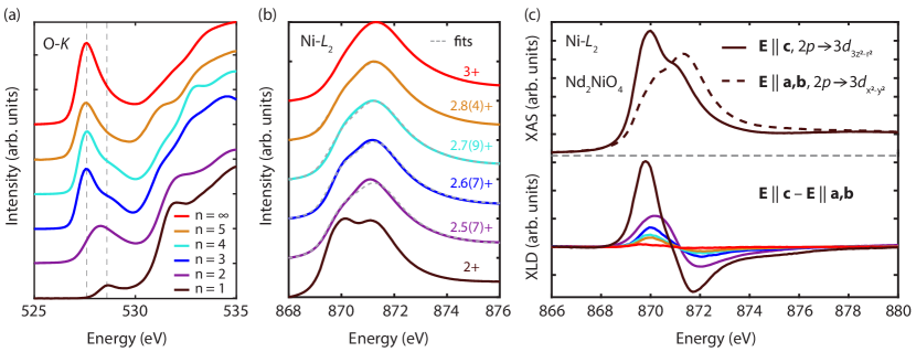
To measure electronic structure changes across the Ruddlesden-Popper series, we use XAS. We start with the O- edges, which can provide a probe of the nickel valence. In particular, we focus on the prepeak, or first peak along the oxygen edge, which arises from the covalent mixing of the oxygen 2 with the nickel 3 states [45]. Due to varying contributions from the LaAlO3 substrate eV, we do not address the higher-energy fine structure features, whereas the lower-energy pre-peak region is free from background features. The full O -edge spectra can be found in Fig. S8 in the Supplemental Material [27]. The intensity of this prepeak across members of a homologous transition metal series should scale with the number of unoccupied 3 states (increasing valence state) as per a 1 to hybridized 2-3 (or 3 type transition) [45, 46]. Here then, Nd2NiO4 with a nominal valence of Ni2+ should have the weakest intensity O prepeak with a minor shift to higher energies representing transitions into states of the type [47, 48, 49]. Meanwhile NdNiO3, with a valence of Ni3+ and a ground state dominated by highly covalent states [50, 51] (nominally ) should have the strongest intensity prepeak, with all intermediate Ruddlesden-Poppers interpolating in-between. Indeed we observe this general trend in pre-peak intensity across our Ndn+1NinO3n+1 samples, as shown in Fig. 3(a). We quantify both the integrated pre-peak intensities, which scale with the nickel-oxygen hybridization levels, and the maximum of the prepeak signal, which reflects the relative number of unoccupied states, as shown in Fig. S8 in the Supplemental Material [27]. In both quantities, and particularly in the estimates of the integrated pre-peak intensities, the differences between the higher order () compounds are within error. This indicates that relative nickel-oxygen hybridization levels do not appreciably change between Ruddlesden-Popper compounds of increasing high order, unlike in their reduced square-planar counterparts [12]. Nevertheless, the general trend of increased pre-peak intensity from = 1 to points to an overall depletion of the nominal nickel 3 states and increasing covalency as we move down the Ruddlesden-Popper series from NdNiO3 () to Nd2NiO4 ( = 1).
To further assess the filling of the nickel 3 states, we can decompose this pre-peak region into the two distinct features demarcated by the dotted grey lines in Fig. 3(a). We assign these features to represent transitions associated with the hybridized (nominal) and states [48, 52]. Accordingly, the mixed-valence Ruddlesden-Poppers () possess spectral weight from both these features with more of the lower energy (higher valence) feature as we increase the dimensionality of the system. This effect has been previously observed in single-layer SrxNiO4 compounds [47, 48], where hole-doping away from Ni2+ toward Ni3+ shifts the total spectral weight of the O prepeak toward lower incident energy in XAS. With the recent observation of superconductivity in a layered nickelate [12] and the identification of inequivalent transition-metal planes in a five-layer cuprate [53], the layer-resolved distribution of the nickel valence is of increasing interest though conflicting reports exist in bulk crystal studies [16, 38]. This observation that the mixed-valence Ruddlesden-Popper compounds possess both Ni2+ and Ni3+ features in the O- edge pre-peak region, in contrast to previous work [54], provides a future means to use spatially resolved spectroscopic techniques such as electron-energy loss spectroscopy to identify any electronic modulation.
The Ni -edges, which we present in Fig. 3(b), are comparatively more difficult to interpret due to core-hole effects [55], and are exquisitely sensitive to variations in the strain state, cation composition, and oxygen content [49, 56, 40, 57]. The strong covalency effects in the oxidized nickelates complicate the quantitative extraction of valence as can be performed in other perovskite oxides such as the titanates or manganites [45, 58, 59]. Nevertheless, we can employ a self-consistent method to characterize the systematic evolution of the nickel valence across the series, as has been similarly performed using x-ray photoemission spectroscopy [20]. We define our spectra from the Nd2NiO4 ( = 1) and NdNiO3 () end-member compounds, which have been well-characterized in the bulk [60, 52], as proxies for the Ni2+ and Ni3+ reference spectra, respectively, within the layered nickelate series. We then use these reference spectra in a non-negative linear least squares fitting to extract the nominal nickel valences as tabulated in Table 1. As the octahedral coordination environments and transition metal–oxygen hybridization should be reasonably similar across the Ruddlesden-Popper nickelates, we expect this approach to be more reflective of relative valence changes than using reference spectra from generic Ni2+ compounds such as NiO. The valences interpolate nearly monotonically between 2+ and 3+ as we move from to and are close to the expected values from simple electron counting rules. (Note that we employ this method on just the higher energy Ni -edges, which are free of the La background from the LaAlO3 substrate that runs into the Ni -edge as seen in Fig. S8 in the Supplemental Material [27].) We attribute deviations from the ideal fractional valences to minor variations in cation stoichiometry and oxygen content which are challenging to quantify precisely in nickelate thin films. Nonetheless, this general procedure reveals the gradation of the nickel filling from formal 3 to 3 across the order of the Ruddlesden-Popper compounds, further indicating that the layering may be harnessed to control the electronic filling of the rare-earth nickelates.
The Ni spectra presented above are polarization averaged; we now decompose them to compare the x-ray linear dichroic (XLD) signals across the series. At the Ni -edge, we expect from dipole selection rules that only 2 transitions are allowed for () and primarily 2 transitions are allowed for () [48]. Hence, assuming Nd2NiO4 () to be in a high-spin state with two half-filled orbitals we expect a large XLD signal arising from a splitting of the and orbitals generated by a strong tetragonal distortion [48, 49]. In contrast, the dichroism in the NdNiO3 () film is negligible: with a single half-filled orbital, no dichroism is expected without substantial strain or heterostructure engineering that breaks the double degeneracy of the orbitals [61, 62, 34, 63]. Thus the XLD of the mixed-valent compounds should decrease going from the single-layer Nd2NiO4 to the perovskite NdNiO3. This is indeed the trend observed experimentally in Fig. 3(c). Compressive strain may also contribute to a slight enhancement of this dichroic response. It has been previously shown in nickelate compounds that in straightening out the NiO6 octahedra in the axis and promoting a tetragonal distortion, compressive strain acts to lower the energy of the orbital and shifts the spectra to lower energy [64, 65, 63]. As we move from the bulk lattice constants of = 3.807 Å in NdNiO3 () [9] to = 3.827 Å in Nd2NiO4 (), the compressive strain increases from to . Hence, our observed trend of an increased XLD signal, with the () peak sitting at lower energy than the (), as we decrease the order of the Ndn+1NinO3n+1 compounds may also reflect the additional effect of compressive epitaxial strain.
III.3 Electrical transport
Having demonstrated the structural and electronic modulations of the Ruddlesden-Popper nickelates as a function of layering order , we now present electrical resistivity measurements for the Ndn+1NinO3n+1 for , in Fig. 4. The compound is insulating as in the bulk, likely due to the presence of a charge-stripe-ordered state [6]. The compound exhibits a near metal-to-insulating transition with minor hysteresis, though we have also observed fully insulating behavior in samples of slightly diminished quality, similar to observations in bulk La3Ni2O7 [66]. The compounds exhibit a metal-to-insulator transition with a hysteresis reminiscent of the perovskite NdNiO3 albeit with a far weaker transition to the insulating state. The transition temperatures span between 87 and 150 K and are generally suppressed with the increasing order of the system although there is slight variation sample to sample. Intriguingly, both the metal-to-insulator transition temperature and magnitude of the resistivity jump through the transition decrease with the increasing order of the system. This is contrary to an expectation that the resistivities of the Ndn+1NinO3n+1, in moving to higher order , would begin to approximate those of the parent NdNiO3 .
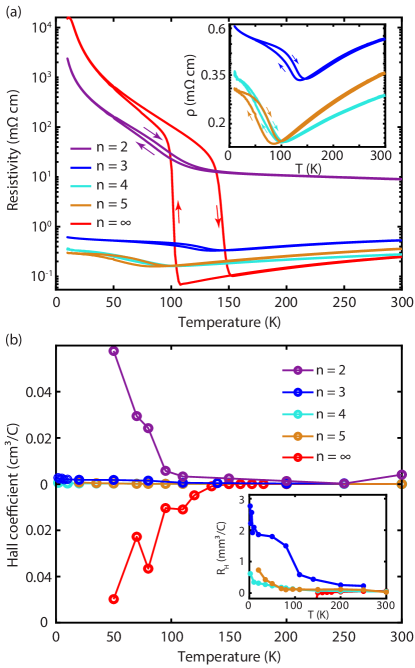
The bulk Ni3O10 compounds possess a second-order metal-to-metal transition at 150 K emblematic of the formation of a charge density wave (CDW) instability [38, 8, 37, 39]. Interestingly, we do not observe this behavior in our Nd4Ni3O10 films stabilized with compressive epitaxial strain, though we have previously found this metal-to-metal transition in thin film Nd4Ni3O10 on NdGaO3 substrates which provide tensile strain [12]. Nevertheless, our compressively strained Nd4Ni3O10 films may still possess a CDW transition that is now manifest as a metal-to-insulator not metal-to-metal transition. The temperature-dependent Hall coefficients exhibit a sharp jump at the transition temperature as shown in Fig. 4(b). This is consistent with bulk measurements reflecting a loss of carriers due a Fermi surface reconstruction and CDW instability in Nd4Ni3O10 [37]. In contrast, the opening of a bond disproportionated gap in the NdNiO3 compounds is reflected in a change in the sign of Hall carriers [67]. Thus it is likely that the epitaxially stabilized Ruddlesden-Popper compounds still possess a CDW transition as in single crystal Nd4Ni3O10 but that compressive epitaxial strain modifies this transition. The precise role of strain on modulating these charge states in these Ruddlesden-Popper compounds would require further investigation. We note that the weak hysteresis and metal-to-insulator transitions – characteristics which qualitatively resemble the resistivity behavior of NdNiO3 – appear intrinsic to thin film Ndn+1NinO3n+1 () stabilized on LaAlO3, as they are reproducible across all high-quality films (see Fig. S5 in the Supplemental Material [27]). These features are likely not due to the presence of trace NdNiO3, as we do not observe large areas with missing rock salt layers in STEM images, as shown in Fig. 2. Finally, the evolution of the temperature-dependent Hall coefficients in Fig. 4(b) suggest that as we increase the order of the system, the low-temperature Hall coefficients decrease and thus, the bands crossing the Fermi level begin to approximate those in the parent NdNiO3 [67]. This points to a potential crossover from the incommensurate CDW in the to the fully charge disproportionated state in the within the range.
IV Conclusions
In summary, we have synthesized epitaxial thin films of the neodymium-based Ruddlesden-Popper nickelates, Ndn+1NinO3n+1 with MBE. Our synthetic strategy carefully optimizes the deposition of the perovskite NdNiO3 to enable the precise layer-by-layer growth of the Ruddlesden-Popper films, and can potentially be generalized to any Ruddlesden-Popper system. XAS at the O- and Ni- edges demonstrate a consistent depletion of the formal nickel 3 states as we move across the series from to . There is also a concomitant increase in the oxygen character as would be expected from increasing valence [68]. XLD suggests that the splitting between the in-plane and out-of-plane orbitals in the manifold increases, consistent with an increased tetragonal distortion toward . In the electronic transport the compounds exhibit a weakly hysteretic metal-to-insulator transition though with resistivity changes small compared with the parent NdNiO3. This resistivity behavior differs from the non-hysteretic, second-order metal-to-metal transitions in bulk NinO3n+1 which are reflective of a CDW instability. The temperature-dependent Hall coefficients however suggest that such a CDW-like transition does occur, but that this transition begins to cross over to the charge-ordered transition in NdNiO3 () as increases. This underscores the apparent sensitivity of these layered nickelates to both epitaxial strain and dimensionality.
Our work invites further exploration of the electronic and magnetic phases in thin film Ruddlesden-Popper systems, and proximate to the superconductivity observed in our reduced Nd6Ni5O12 compound [12]. For example, bulk single-crystal specimens of Nd4Ni3O10 exhibit intertwined charge and spin density waves [18]. Investigating the coupling of charge and spin order in the layered nickelates would thus be an exciting future pursuit, facilitated by the successful synthesis of thin-film Ruddlesden-Popper nickelates. Finally, synthesis of Ndn+1NinO3n+1 thin films provides a platform to search for additional superconductivity in the square-planar Ndn+1NinO2n+2 compounds.
Acknowledgments
We thank H. Hijazi at the Rutgers University Laboratory of Surface Modification for assistance in Rutherford backscattering spectrometry. Research is primarily supported by the US Department of Energy (DOE), Office of Basic Energy Sciences, Division of Materials Sciences and Engineering, under Award No. DE-SC0021925. Materials growth was supported by PARADIM under National Science Foundation (NSF) Cooperative Agreement No. DMR-2039380. Electron microscopy was primarily carried out through the use of MIT.nano facilities at the Massachusetts Institute of Technology. Additional electron microscopy and all nanofabrication work was performed at Harvard University’s Center for Nanoscale Systems, a member of the National Nanotechnology Coordinated Infrastructure Network, supported by the NSF under Grant No. 2025158. In this paper, we also used resources of the Advanced Light Source, a DOE Office of Science User Facility under Contract No. DE-AC02-05CH11231. G.A.P. acknowledges support from the Paul & Daisy Soros Fellowship for New Americans and from NSF Graduate Research Fellowship Grant No. DGE-1745303. Q.S. and D.C.C. were supported by the Science and Technology Center for Integrated Quantum Materials, NSF Grant No. DMR-1231319. M.-C.J and A.S.B. acknowledge NSF Grant No. DMR-2045826 and the ASU Research Computing Center for high-performance computing resources. H.E.S. and I.E. were supported by the Rowland Institute at Harvard. E.E.F., B.H.G., and L.F.K. were supported by the NSF (PARADIM) under Cooperative Agreement No. DMR-2039380. J.A.M acknowledges support from the Packard Foundation and the Gordon and Betty Moore Foundation’s EPiQS Initiative, Grant No. GBMF6760.
G.A.P. and Q.S. contributed equally to this work.
References
- Torrance et al. [1992] J. B. Torrance, P. Lacorre, A. I. Nazzal, E. J. Ansaldo, and C. Niedermayer, Phys. Rev. B 45, 8209 (1992).
- Catalano et al. [2018] S. Catalano, M. Gibert, J. Fowlie, J. Iniguez, J.-M. Triscone, and J. Kreisel, Reports on Progress in Physics 81, 046501 (2018).
- Sreedhar et al. [1992] K. Sreedhar, J. Honig, M. Darwin, M. McElfresh, P. Shand, J. Xu, B. Crooker, and J. Spalek, Physical Review B 46, 6382 (1992).
- Liu et al. [2020] C. Liu, V. F. Humbert, T. M. Bretz-Sullivan, G. Wang, D. Hong, F. Wrobel, J. Zhang, J. D. Hoffman, J. E. Pearson, J. S. Jiang, C. Chang, A. Suslov, N. Mason, M. R. Norman, and A. Bhattacharya, Nat. Commun. 11, 1402 (2020).
- Rodriguez-Carvajal et al. [1991] J. Rodriguez-Carvajal, M. Fernandez-Diaz, and J. Martinez, Journal of Physics: Condensed Matter 3, 3215 (1991).
- Emery et al. [1999] V. J. Emery, S. A. Kivelson, and J. M. Tranquada, Proc. Natl Acad. Sci. 96, 8814 (1999).
- Keimer et al. [2015] B. Keimer, S. A. Kivelson, M. R. Norman, S. Uchida, and J. Zaanen, Nature 518, 179 (2015).
- Greenblatt [1997] M. Greenblatt, Curr Opin Solid State Mater Sci 2, 174 (1997).
- Lacorre et al. [1991] P. Lacorre, J. Torrance, J. Pannetier, A. Nazzal, P. Wang, and T. Huang, J. Solid State Chem. 91, 225 (1991).
- Zhang et al. [2017] J. Zhang, A. S. Botana, J. W. Freeland, D. Phelan, H. Zheng, V. Pardo, M. R. Norman, and J. F. Mitchell, Nat. Phys. 13, 864 (2017).
- Li et al. [2019] D. Li, K. Lee, B. Y. Wang, M. Osada, S. Crossley, H. R. Lee, Y. Cui, Y. Hikita, and H. Y. Hwang, Nature 572, 624 (2019).
- Pan et al. [2022] G. A. Pan, D. Ferenc Segedin, H. LaBollita, Q. Song, E. M. Nica, B. H. Goodge, A. T. Pierce, S. Doyle, S. Novakov, D. Córdova Carrizales, et al., Nature Materials 21, 160 (2022).
- Zhang and Greenblatt [1995] Z. Zhang and M. Greenblatt, Journal of Solid State Chemistry 117, 236 (1995).
- Seo et al. [1996] D.-K. Seo, W. Liang, M.-H. Whangbo, Z. Zhang, and M. Greenblatt, Inorganic chemistry 35, 6396 (1996).
- Poltavets et al. [2006] V. V. Poltavets, K. A. Lokshin, T. Egami, and M. Greenblatt, Materials Research Bulletin 41, 955 (2006).
- Zhang et al. [2020a] J. Zhang, H. Zheng, Y.-S. Chen, Y. Ren, M. Yonemura, A. Huq, and J. F. Mitchell, Phys. Rev. Mater. 4, 083402 (2020a).
- Li et al. [2017] H. Li, X. Zhou, T. Nummy, J. Zhang, V. Pardo, W. E. Pickett, J. F. Mitchell, and D. S. Dessau, Nat. Commun. 8, 1 (2017).
- Zhang et al. [2020b] J. Zhang, D. Phelan, A. S. Botana, Y.-S. Chen, H. Zheng, M. Krogstad, S. G. Wang, Y. Qiu, J. Rodriguez-Rivera, R. Osborn, S. Rosenkranz, M. R. Norman, and J. F. Mitchell, Nat. Commun. 11, 6003 (2020b).
- Li et al. [2020a] Z. Li, W. Guo, T. T. Zhang, J. H. Song, T. Y. Gao, Z. B. Gu, and Y. F. Nie, APL Mater. 8, 091112 (2020a).
- Sun et al. [2021] W. Sun, Y. Li, X. Cai, J. Yang, W. Guo, Z. Gu, Y. Zhu, and Y. Nie, Physical Review B 104, 184518 (2021).
- Dawley et al. [2020] N. M. Dawley, B. H. Goodge, W. Egger, M. R. Barone, L. F. Kourkoutis, D. J. Keeble, and D. G. Schlom, Appl. Phys. Lett. 117, 062901 (2020).
- Brooks et al. [2009] C. M. Brooks, L. F. Kourkoutis, T. Heeg, J. Schubert, D. A. Muller, and D. G. Schlom, Applied Physics Letters 94, 162905 (2009).
- Barone et al. [2021] M. R. Barone, N. M. Dawley, H. P. Nair, B. H. Goodge, M. E. Holtz, A. Soukiassian, E. E. Fleck, K. Lee, Y. Jia, T. Heeg, R. Gatt, Y. Nie, D. A. Muller, L. F. Kourkoutis, and D. G. Schlom, APL Mater. 9, 021118 (2021).
- Haeni et al. [2000] J. Haeni, C. D. Theis, and D. G. Schlom, Journal of Electroceramics 4, 385 (2000).
- Li et al. [2021] Y. Li, W. Sun, J. Yang, X. Cai, W. Guo, Z. Gu, Y. Zhu, and Y. Nie, Frontiers in Physics 9, 443 (2021).
- Sun et al. [2022] J. Sun, C. T. Parzyck, J. H. Lee, C. M. Brooks, L. F. Kourkoutis, X. Ke, R. Misra, J. Schubert, F. V. Hensling, M. R. Barone, et al., Physical Review Materials 6, 033802 (2022).
- [27] See Supplemental Material for additional structural and electronic characterization.
- Breckenfeld et al. [2014] E. Breckenfeld, Z. Chen, A. R. Damodaran, and L. W. Martin, ACS Appl. Mater. Interfaces 6, 22436 (2014).
- Preziosi et al. [2017] D. Preziosi, A. Sander, A. Barthélémy, and M. Bibes, AIP Advances 7, 015210 (2017).
- El Baggari et al. [2018] I. El Baggari, B. H. Savitzky, A. S. Admasu, J. Kim, S.-W. Cheong, R. Hovden, and L. F. Kourkoutis, Proceedings of the National Academy of Sciences 115, 1445 (2018).
- Goodge et al. [2022] B. H. Goodge, I. El Baggari, S. S. Hong, Z. Wang, D. G. Schlom, H. Y. Hwang, and L. F. Kourkoutis, Microscopy and Microanalysis , 1 (2022).
- Fleck et al. [2022] E. E. Fleck, B. H. Goodge, M. R. Barone, H. P. Nair, N. J. Schreiber, N. M. Dawley, D. G. Schlom, and L. F. Kourkoutis, unpublished (2022).
- Wu et al. [2004] W. Wu, D. Huang, G. Guo, H.-J. Lin, T. Hou, C. Chang, C. Chen, A. Fujimori, T. Kimura, H. Huang, et al., Journal of electron spectroscopy and related phenomena 137, 641 (2004).
- Wu et al. [2013] M. Wu, E. Benckiser, M. Haverkort, A. Frano, Y. Lu, U. Nwankwo, S. Brück, P. Audehm, E. Goering, S. Macke, , G. Logvenov, H. Habermeier, and B. Keimer, Physical Review B 88, 125124 (2013).
- Nelson and Riley [1945] J. B. Nelson and D. P. Riley, Proc. Phys. Soc. 57, 160 (1945).
- Burganov et al. [2016] B. Burganov, C. Adamo, A. Mulder, M. Uchida, P. King, J. Harter, D. Shai, A. Gibbs, A. Mackenzie, R. Uecker, et al., Physical Review Letters 116, 197003 (2016).
- Li et al. [2020b] Q. Li, C. He, X. Zhu, J. Si, X. Fan, and H.-H. Wen, Sci. China Phys. Mech. Astron. 64, 227411 (2020b).
- Li et al. [2020c] B.-Z. Li, C. Wang, P. T. Yang, J. P. Sun, Y.-B. Liu, J. Wu, Z. Ren, J.-G. Cheng, G.-M. Zhang, and G.-H. Cao, Phys. Rev. B 101, 195142 (2020c).
- Rout et al. [2020] D. Rout, S. R. Mudi, M. Hoffmann, S. Spachmann, R. Klingeler, and S. Singh, Phys. Rev. B 102, 195144 (2020).
- Kim et al. [2020] T. Kim, T. Paudel, R. Green, K. Song, H.-S. Lee, S.-Y. Choi, J. Irwin, B. Noesges, L. Brillson, M. Rzchowski, G. Sawatzky, E. Tsymbal, and C. Eom, Physical Review B 101, 121105 (2020).
- Lee et al. [2013] C.-H. Lee, N. D. Orloff, T. Birol, Y. Zhu, V. Goian, E. Rocas, R. Haislmaier, E. Vlahos, J. A. Mundy, L. F. Kourkoutis, Y. Nie, M. D. Biegalski, J. Zhang, M. Bernhagen, N. A. Benedek, Y. Kim, J. D. Brock, R. Uecker, X. X. Xi, V. Gopalan, D. Nuzhnyy, S. Kamba, D. A. Muller, I. Takeuchi, J. C. Booth, C. J. Fennie, and D. G. Schlom, Nature 502, 532 (2013).
- Lee et al. [2014] J. H. Lee, G. Luo, I. C. Tung, S. H. Chang, Z. Luo, M. Malshe, M. Gadre, A. Bhattacharya, S. M. Nakhmanson, J. A. Eastman, H. Hong, J. Jellinek, D. Morgan, D. D. Fong, and J. W. Freeland, Nat. Mater. 13, 879 (2014).
- Nie et al. [2014] Y. Nie, Y. Zhu, C.-H. Lee, L. F. Kourkoutis, J. A. Mundy, J. Junquera, P. Ghosez, D. Baek, S. Sung, X. Xi, et al., Nature Communications 5, 1 (2014).
- Nair et al. [2018] H. P. Nair, J. P. Ruf, N. J. Schreiber, L. Miao, M. L. Grandon, D. J. Baek, B. H. Goodge, J. P. C. Ruff, L. F. Kourkoutis, K. M. Shen, and D. G. Schlom, APL Mater. 6, 101108 (2018).
- de Groot et al. [1989] F. M. F. de Groot, M. Grioni, J. C. Fuggle, J. Ghijsen, G. A. Sawatzky, and H. Petersen, Phys. Rev. B 40, 5715 (1989).
- Suntivich et al. [2014] J. Suntivich, W. T. Hong, Y.-L. Lee, J. M. Rondinelli, W. Yang, J. B. Goodenough, B. Dabrowski, J. W. Freeland, and Y. Shao-Horn, J. Phys. Chem. C 118, 1856 (2014).
- Kuiper et al. [1991] P. Kuiper, J. Van Elp, G. Sawatzky, A. Fujimori, S. Hosoya, and D. De Leeuw, Physical Review B 44, 4570 (1991).
- Pellegrin et al. [1996] E. Pellegrin, J. Zaanen, H.-J. Lin, G. Meigs, C. Chen, G. Ho, H. Eisaki, and S. Uchida, Physical Review B 53, 10667 (1996).
- Kuiper et al. [1998] P. Kuiper, J. Van Elp, D. Rice, D. Buttrey, H.-J. Lin, and C. Chen, Physical Review B 57, 1552 (1998).
- Mizokawa et al. [2000] T. Mizokawa, D. Khomskii, and G. Sawatzky, Physical Review B 61, 11263 (2000).
- Bisogni et al. [2016] V. Bisogni, S. Catalano, R. J. Green, M. Gibert, R. Scherwitzl, Y. Huang, V. N. Strocov, P. Zubko, S. Balandeh, J.-M. Triscone, G. Sawatzky, and T. Schmitt, Nat. Commun. 7, 13017 (2016).
- Hu et al. [2000] Z. Hu, M. Golden, J. Fink, G. Kaindl, S. Warda, D. Reinen, P. Mahadevan, and D. Sarma, Physical Review B 61, 3739 (2000).
- Kunisada et al. [2020] S. Kunisada, S. Isono, Y. Kohama, S. Sakai, C. Bareille, S. Sakuragi, R. Noguchi, K. Kurokawa, K. Kuroda, Y. Ishida, S. Adachi, R. Sekine, T. K. Kim, C. Cacho, S. Shin, T. Tohyama, K. Tokiwa, and T. Kondo, Science 369, 833 (2020).
- Di Pietro et al. [2021] P. Di Pietro, M. Golalikhani, K. Wijesekara, S. K. Chaluvadi, P. Orgiani, X. Xi, S. Lupi, and A. Perucchi, ACS Applied Materials & Interfaces 13, 6813 (2021).
- Fink et al. [1985] J. Fink, T. Müller-Heinzerling, B. Scheerer, W. Speier, F. Hillebrecht, J. Fuggle, J. Zaanen, and G. Sawatzky, Physical Review B 32, 4899 (1985).
- Freeland et al. [2016] J. W. Freeland, M. van Veenendaal, and J. Chakhalian, J. Electron Spectrosc. 208, 56 (2016).
- Tung et al. [2017] I.-C. Tung, G. Luo, J. H. Lee, S. H. Chang, J. Moyer, H. Hong, M. J. Bedzyk, H. Zhou, D. Morgan, D. D. Fong, and J. W. Freeland, Physical Review Materials 1, 053404 (2017).
- Kourkoutis et al. [2010] L. F. Kourkoutis, H. Xin, T. Higuchi, Y. Hotta, J. Lee, Y. Hikita, D. Schlom, H. Hwang, and D. Muller, Philosophical Magazine 90, 4731 (2010).
- Mundy et al. [2014] J. A. Mundy, Y. Hikita, T. Hidaka, T. Yajima, T. Higuchi, H. Y. Hwang, D. A. Muller, and L. F. Kourkoutis, Nature Communications 5, 1 (2014).
- Piamonteze et al. [2005] C. Piamonteze, F. De Groot, H. Tolentino, A. Ramos, N. Massa, J. Alonso, and M. Martínez-Lope, Physical Review B 71, 020406 (2005).
- Chaloupka and Khaliullin [2008] J. Chaloupka and G. Khaliullin, Phys. Rev. Lett. 100, 016404 (2008).
- Disa et al. [2015a] A. S. Disa, D. P. Kumah, A. Malashevich, H. Chen, D. A. Arena, E. D. Specht, S. Ismail-Beigi, F. J. Walker, and C. H. Ahn, Phys. Rev. Lett. 114, 026801 (2015a).
- Disa et al. [2015b] A. S. Disa, F. Walker, S. Ismail-Beigi, and C. H. Ahn, APL Materials 3, 062303 (2015b).
- Freeland et al. [2011] J. Freeland, J. Liu, M. Kareev, B. Gray, J. Kim, P. Ryan, R. Pentcheva, and J. Chakhalian, Europhysics Letters 96, 57004 (2011).
- Tung et al. [2013] I.-C. Tung, P. Balachandran, J. Liu, B. Gray, E. Karapetrova, J. Lee, J. Chakhalian, M. Bedzyk, J. Rondinelli, and J. Freeland, Physical Review B 88, 205112 (2013).
- Zhang et al. [1994] Z. Zhang, M. Greenblatt, and J. Goodenough, Journal of Solid State Chemistry 108, 402 (1994).
- Hauser et al. [2013] A. J. Hauser, E. Mikheev, N. E. Moreno, T. A. Cain, J. Hwang, J. Y. Zhang, and S. Stemmer, Applied Physics Letters 103, 182105 (2013).
- Zaanen et al. [1985] J. Zaanen, G. A. Sawatzky, and J. W. Allen, Phys. Rev. Lett. 55, 418 (1985).