Single-Shot Optical Neural Network
††journal: osajournal††articletype: Research ArticleAs deep neural networks (DNNs) grow to solve increasingly complex problems, they are becoming limited by the latency and power consumption of existing digital processors. For improved speed and energy efficiency, specialized analog optical and electronic hardware has been proposed, however, with limited scalability (input vector length of hundreds of elements). Here, we present a scalable, single-shot-per-layer analog optical processor that uses free-space optics to reconfigurably distribute an input vector and integrated optoelectronics for static, updatable weighting and the nonlinearity — with and beyond. We experimentally test classification accuracy of the MNIST handwritten digit dataset, achieving 94.7% (ground truth 96.3%) without data preprocessing or retraining on the hardware. We also determine the fundamental upper bound on throughput (0.9 exaMAC/s), set by the maximum optical bandwidth before significant increase in error. Our combination of wide spectral and spatial bandwidths in a CMOS-compatible system enables highly efficient computing for next-generation DNNs.
1 Introduction
Artificial deep neural networks (DNNs) have revolutionized automated image classification [1], natural language processing [2] and medical prediction and diagnosis [3]. These breakthroughs were made possible by sufficiently large datasets and computing capacity, since an increase in DNN model size tends to yield higher accuracy [4, 5]. Recently, though specialized digital hardware has significantly improved the latency, energy consumption and throughput of deep learning [6, 7], the computation and memory costs of modern DNNs have continued to grow exponentially, outpacing the Moore’s law increases in microprocessor performance [4]. Inference, which accounts for 80-90% of machine learning tasks in data centers [8], has particularly stringent requirements for low latency, such as in translation and autonomous driving, as well as in newer applications in astrophysics [9] and the control of fusion reactors [10].
The rate-limiting step in DNN inference is matrix-vector multiplication (MVM), which implements the synaptic connections in a network layer: a matrix of learned weights multiplies an input vector of length (which often exceeds ,000 in modern DNN workloads [5]). Within MVM, the most expensive task is data movement of the weights and inputs from memory to the multiplier units, followed by the multiply-accumulate (MAC) operation itself [7, 11]. Static, ‘weight-stationary’ architectures [11] (e.g., in-memory computing [12]) can yield significant improvements in efficiency, since in this dataflow, the input vector is broadcast across the multiplier units that apply fixed weights, and the output vector can, in theory, be read out in one step. DNN layer outputs can thus be computed in a single shot without costly weight updates if the entire weight matrix can be stored on the hardware.
A survey of previous weight-stationary DNN accelerators [7, 13, 14, 15, 16, 17] reveals a tradeoff between latency, energy consumption, and scalability, i.e., the number of weights that the hardware can accommodate. In digital electronic circuits (e.g., Google’s Tensor Processing Unit, or TPU [7]), constraints on wiring for digital data transmission require partial products to be passed from one multiplier to the next at each clock cycle, which prohibits single-shot MVM. Analog electronic circuits such as memristor crossbar arrays [13], on the other hand, can sum partial products along a wire by Kirchhoff’s current law, but they are bounded in speed, energy consumption and accuracy by parasitic capacitance, resistance, and current leakage [18]. Integrated 2D optical schemes can compute at still higher speeds [15, 16, 17], but limits on control, multiplexing, component area and on-chip losses through -depth circuits constrain scalability to a vector length of hundreds of elements.
A 3D optical architecture permits greater connectivity between potentially millions of spatial modes [19, 20], given the prevalence of megapixel-scale optoelectronic components (e.g., cameras and spatial light modulators). 3D optical MVM accelerators were among the first to be investigated by pioneers in the field [21, 22, 23, 24] — partly out of necessity prior to the advent of compact low-loss photonic integrated circuits — but they did not achieve widespread adoption for two reasons. First, competition from digital electronic computers limited their application space [25]. Second, they suffered from a lack of flexibility, as experimental demonstrations employed fixed weighting masks or bulky modulators and were small in scale (input vectors with 10s of elements). Recently, theoretical analyses showing the potential of ultra-low-energy computing for DNNs (e.g., [26]) have driven a resurgent interest in 3D optical processors; however, experimental realizations have been limited to vector-vector dot products [27], MVM at small scale ( elements) [28], and diffractive / convolutional models with limited matrix expressivity [29, 30, 31, 32].
Here, we present for the first time a demonstration of a fully programmable, 3D optical neural network (ONN) capable of single-shot-per-layer inference at large scale. Optical sources encode an input vector and free-space optical components copy and distribute this display (fan-out) to updatable optoelectronic weighting elements. Electronics sum the partial products and implement the nonlinearity. We thus combine the advantages of free-space optics (tightly packed spatial modes) and integrated optoelectronics (reconfigurable weighting and a low-power nonlinearity) to enable scalability. We show high classification accuracy of the MNIST handwritten digit dataset in a proof-of-concept experiment with , where dynamic reconfigurability of the inputs, fan-out and weighting elements allow for potential model updates. We then determine the physical limit to throughput of our system (0.9 exaMAC/s) by measuring classification accuracy versus source spectral width. Lastly, we calculate the theoretical total latency (10 ns), energy consumption (10 fJ/MAC) and throughput (petaMAC/s) to process a complete million-element DNN layer (with 000) with near-term, CMOS-compatible technologies. This highly efficient architecture can enable next-generation DNNs while also having a significant impact on other fields such as non-convex optimization (e.g., Ising problems), signal processing and other machine-learning tasks where MVM also dominates energy consumption and latency.

2 Concept
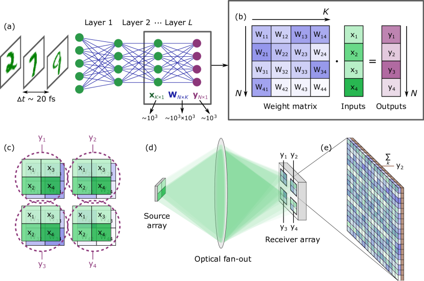
As illustrated in Fig. 1, the key feature of our architecture is the ability to compute a DNN inference layer in a single shot. In a fully connected neural network (Fig. 1a,b), a layer’s output elements (y) are the weighted sums of the inputs (x), cascaded into a nonlinear activation function () that approximates the thresholding operation in the brain [11]. In other words, a fully connected layer is equivalent to an MVM, with , where the weights (W) have been pre-learned during the training phase. Convolutional layers can also be implemented by matrix multiplication, e.g., using a Toeplitz matrix [11]. In Fig. 1c, x and the rows of W are both recast into blocks, with x projected onto each row of W. In the case of a 2D input image, x is already in block form. With the inputs then local to their corresponding weights, all required element-wise multiplications are completed simultaneously. Free-space optics can passively realize this data routing, replication and weighting (Fig. 1d,e).
In our proposed architecture, a 4 lens system performs the single-shot MVM (Fig. 2). A source array encodes the input activations into the single-spatial-mode analog amplitudes of light pulses in the object plane ), where r is the transverse spatial position in the 2D source plane. These sources can operate at GHz rates using vertical-cavity surface-emitting lasers (VCSELs) [33], LEDs [34] or emerging high-speed spatial light modulators (SLMs) [35]. In the Fourier plane, a diffractive optical element (DOE), e.g., a liquid crystal on silicon (LCoS) SLM, displays a spot array generation phase pattern for reconfigurable fan-out. Following Fourier convolution theory, the spot array in the image plane generated by the DOE is optically convolved with the image of the input pattern, which yields copies of the input pattern. Reconfigurable weighting elements, e.g., LCoS SLM pixels plus a polarizer, then attenuate the intensity of each replicated input pixel proportionally to each weight value in W. m-scale photodetectors (PDs) [36, 37] directly below the weighting elements can convert the signal to analog electronics for block-wise summation by Kirchhoff’s current law. With ‘optical fan-in’ [27], a single large PD can replace the block of small, electrically connected PDs. An amplifier per block reads out the accumulated charge and an electronic post-processing unit performs the nonlinearity to yield y. An output source array (e.g., same components as the input sources) with one source per block can then be the input to the next layer.
3 Results
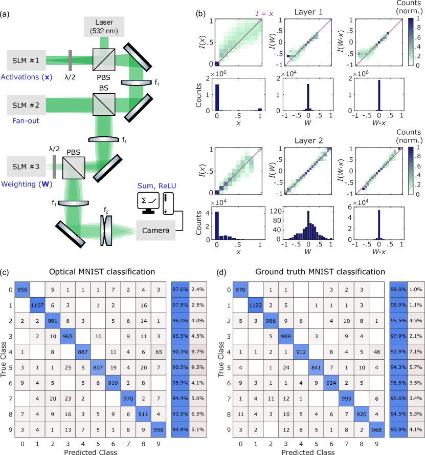
We experimentally verified the impact of single-shot analog optical data encoding, fan-out and weighting on the classification accuracy of the MNIST handwritten digit dataset [38]. We used a two-hidden-layer fully connected neural network (FC-NN) with activations (see Methods for the training procedure on a digital electronic computer). Figure 3a provides a schematic representation of our setup, where three LCoS SLMs display a complete activation image (SLM #1), fan-out pattern (SLM #2) and full weight matrix (SLM #3) for multiplications per frame (see Methods and Supplementary Note 1 for details on the optical system). As a stand-in for an analog electronic circuit, a digital electronic computer performs the per-block summation and nonlinearity.
In Fig. 3b, we show histograms of measured intensities versus transmitted inputs x, weights W and element-wise products . To evaluate , we displayed a different MNIST test image at each time step for 100 steps on SLM #1, set all SLM #3 pixels to a constant, uniform value, and recorded the outputs. Similarly, to measure , we displayed the layer weights on SLM #3 and set all SLM #1 input pixels to a constant, uniform value. For , SLM #1 encoded 100 MNIST test images while SLM #3 displayed the weight matrix. The distribution versus for layer 1 is broad for , but these columns only represent 0.06% of the total counts. Otherwise, is close to the diagonal, i.e., . The distributions for layer 2 are narrower than those for layer 1 due to increased pixel spacing made possible by fewer input activations (see Supplementary Note 1), which lowers crosstalk.
Figure 3c,d shows confusion matrices for inference on 10,000 previously unseen MNIST test images with the two-hidden-layer FC-NN described above. We computed each layer consecutively on the hardware, where camera outputs were fed back to SLM #1 as inputs to the next layer. Thus, the fan-out pattern on SLM #2 was held constant for the duration of the experiment, the weights on SLM #3 were updated only between layers, and the inputs on SLM #1 were refreshed at every time step with each new input vector. We obtained a 94.7% classification accuracy (Fig 3c), compared with the ground-truth all-electronic accuracy of 96.3% (Fig. 3d). Our optical hardware’s classification error was 1% higher than the ground truth for most digits, but up to 4% higher for the digit ‘5’ (additionally misclassified ‘5’s were mostly labeled ‘6’ or ‘8’ by our system, possibly due to blurring from crosstalk). The top-2 optical accuracy was 98.1%, similar to the ground-truth top-2 accuracy of 98.7%.
Next, we investigated the optical limit to throughput of our system. The clock rate is fundamentally limited by source bandwidth, where a broader laser can produce shorter pulses. But a wide spectrum yields blurred outputs: by the spatial Fourier transform relationship between the Fourier and image planes, the distance between each replicated input pattern and the optical axis is linear in wavelength (see Methods). Therefore, the classification error increases with bandwidth, which we verified experimentally by repeating the inference experiment described above with a tunable supercontinuum source in the place of the CW laser (Fig. 4, measured and simulated errors and , respectively). We classified 1,000 images from the MNIST test set with the same two-hidden-layer DNN at different spectral widths (2: twice the RMS width of the spectrum, i.e., twice the standard deviation, to account for the spectrum’s irregular shape). Since our system supports a limited wavelength band, we also simulated the error that would result from Gaussian spectra with broader bandwidths (). Due to optical crosstalk, for a given spectrum, , but follows a similar trend to (shifted to lower 2). Furthermore, doubles from 5.4% with the CW diode to 11% at 2 nm, which we define as the widest acceptable source bandwidth for preserved accuracy. The Fourier transform of the corresponding source spectrum yields a pulse of full width at half maximum 0.02 ps. Therefore, given a transform-limited source in an optimized implementation, the maximum throughput in the first layer is the number of multiply-accumulate operations (19,600) divided by the minimum pulse length, which yields 0.9 exaMAC/s. Emerging high-speed modulators, e.g., plasmonic electro-optic modulators [39], slow-light silicon modulators [40] or thin-film lithium niobate [41], could potentially allow us to achieve this near-exascale throughput.

4 Discussion
We have introduced a scalable optical neural network that can compute DNN layer outputs in a single shot. In our proof-of-concept experiment, we demonstrated low loss of classification accuracy on the MNIST handwritten digit dataset with analog optical data encoding, fan-out and weighting (94.7% optical versus 96.3% ground truth). We also used a filtered supercontinuum source to find that a minimum pulse duration of 0.02 ps maintains the classification error within a factor of two — yielding a near-exascale throughput limit. To improve accuracy, we can reduce stray light on the detector: for example, higher fill-factor SLMs can lessen reflection from their backplanes, aberration-corrected lenses can focus spots more tightly in the image planes to lower crosstalk, and better optical coatings can decrease unwanted interference fringes. We can also use wider and deeper DNNs (i.e., more neurons per hidden layer, a greater number of hidden layers and added biases). Additionally, we plan to benchmark our system against other accelerators with standard DNNs such as LeNet [42] and AlexNet [1]. We obtained all above results without retraining on the hardware, which is preferred since retraining every processor on a large scale, e.g., in data centers, would be resource-intensive. However, to preserve accuracy for broader source spectra, we could modify our DNN model with simulated blurred images as inputs during the training phase.
Having shown that the single-shot ONN can have a small impact on DNN accuracy, the next step will be to demonstrate an implementation optimized for high throughput and low energy consumption. In Methods and Supplementary Note 2, we estimate the latency, throughput, energy and area of a near-term, CMOS-compatible system. Its latency is limited by the optical time of flight (10 ns) and its full-utilization throughput is 1 million MACs per electronic clock cycle (petaMAC/s). Table 1 contrasts these values to digital electronics and output-stationary dataflows, in which the inputs have to be streamed in over time, resulting in a latency that is two orders of magnitude greater for 000. In other DNN accelerators that have limited scalability, matrices that do not fit onto the hardware must be fetched from memory over multiple time steps, subjecting them to the same ‘memory wall’ that currently bottlenecks digital electronics.
In energy consumption, at 10 fJ/MAC, the optimized single-shot ONN can outperform digital electronics by 1-2 orders of magnitude, including sources, detectors, digital-to-analog converters (DAC), analog-to-digital converters (ADC), SLMs, transimpedance amplifiers (TIAs) and electronic nonlinearities (see Methods). To further reduce energy consumption, as the DOE and weights are only updated when the model changes, the fan-out and weighting LCoS SLMs could be replaced with elements that have zero static power consumption, e.g., with an array of optical phase change material cells [43, 44, 45], a fixed phase mask or MEMS modulators [46]. Alternatively, the LCoS SLMs can be optimized for low power consumption [35]. With an increase in source and detector efficiencies [19], the overall energy consumption could then reach the single-femtojoule per MAC regime. DAC and ADC costs may also be eliminated with analog electronic nonlinearities [18], as analog output activations from one layer can be directly used as inputs to the next layer. The inputs to the first layer may also be in the analog domain, e.g., as they are read out from a sensor. In terms of footprint, with bulk optics, the single-shot ONN does consume more overall volume than digital electronic accelerators, but this volume does not contribute to fabrication cost and can be used for air cooling between racks. (The system can also be more compact with shorter-focal-length, aberration-corrected lenses.) The chip area (30 mm2), on the other hand, is similar to digital electronics (25-64 mm2).
| Dataflow | Latency4 (ns) | Throughput4,5 |
| Weight-stationary (near-term)1 | 10 | petaMAC/s |
| Weight-stationary (physical limit)2 | 10 | 19,600/.02 ps exaMAC/s |
| Systolic array (e.g., TPU [7])3 | ,000 | petaMAC/s |
| Output-stationary (e.g., [26]) | ,000 | petaMAC/s |
-
1
Our proposed near-term optimized single-shot ONN (CMOS-compatible).
-
2
From maximum throughput measurements in Results.
-
3
In practice, (throughput 100 teraMAC/s) in the TPU due to wiring and utilization constraints [7].
-
4
Assuming ,000.
-
5
Assuming 100% utilization.
In summary, we have presented a single-shot-per-layer inference machine and demonstrated low loss of classification accuracy with analog, reconfigurable optical matrix-vector multiplication. Coupled to its CMOS manufacturability, our ONN’s extreme parallelism and low resource consumption (enabled by optics) make it a viable, near-term candidate to overcome the compute bottlenecks of state-of-the-art electronics, at scale. Extensions may include spectral multiplexing to further increase scaling or to compute multiple layer or channel outputs simultaneously. With such an efficient DNN processor available to computer scientists, new, larger DNN models may be developed, facilitating the next generation of artificial intelligence.
Methods
Deep neural network training
The FC-NN was trained on a standard digital computer in Python with the Keras library on a subset of the MNIST training set (50,000 images, where 10,000 images were reserved as a validation set to fine-tune the network hyperparameters and optical setup). L1 and L2 regularization with L1 = L2 = 0.0001, 3% Gaussian noise and 10% dropout were applied to each layer. The nonlinear activation function on the final layer was softmax. The Adam optimizer minimized the categorical cross-entropy loss function for 30 epochs.
Experimental setup
An LCoS SLM followed by a polarizing beamsplitter (PBS) displays an input image x by pixel-wise amplitude modulation of a collimated 532 nm continuous-wave (CW) laser diode. In the Fourier plane, a second LCoS phase mask — calculated using the fixed-phase weighted Gerchberg-Saxton algorithm [47] — fans out the input. In the image plane, a third LCoS SLM (also followed by a PBS) displays a complete weight matrix for pixel-wise attenuation (multiplication) of the replicated inputs. The third SLM is imaged onto a camera using additional relay optics (Fig. 3a). The camera is connected to a digital electronic computer that controls the hardware, sums each block of weighted inputs and performs the nonlinearity (Rectified Linear Unit, ReLU). The electronic computer also takes the output pixel values that should be negatively weighted and multiplies them by , as the SLM can only apply the absolute values of the weights. In practice, this negative weighting can be implemented with an analog switch or two PDs per receiver pixel (see Supplementary Note 3). The layer outputs, which are always positive because of the ReLU nonlinearity, are then fed back to the first SLM, and the weights are updated for the next layer of computation. See Supplementary Note 4 for our image processing and one-time system calibration procedures. See Supplementary Note 1 for additional experimental details.
Theoretical classification accuracy with broad source
An LCoS SLM imparts a phase shift of to an incident optical field, with:
| (1) |
where is voltage, is wavelength, is induced extraordinary refractive index (modulated by ), is ordinary refractive index and is liquid crystal thickness [48]. applies to the incident field’s polarization component that is parallel to the extraordinary axis.
Because SLMs #1 and #3, in ‘amplitude mode’, are imaged to the camera, a change in wavelength will simply affect their contrast, and the SLM calibration performed at = 532 nm for output optical intensity versus input value will no longer be perfectly linear. For SLM #2, in phase mode, there is a slight loss of phase contrast for wavelengths different from 532 nm. The main source of error, however, arises because the fan-out spot pattern on the camera, I(, is the spatial Fourier transform of the pattern on SLM #2, , with an argument of . Therefore, at different wavelengths, though the spatial Fourier transform function remains the same, the argument changes:
| (2) |
The distance between the zero order and each diffracted spot (i.e., the center of each input replica) thus increases linearly with wavelength under the paraxial approximation. The height and width of each individual input replica, on the other hand, stays constant since SLM #1 is imaged to the camera, and any chromatic aberration would cause slight blurring from a shift in the position of the focal plane rather than a change in magnification.
To simulate the blurring of each replicated input image due to the spatial Fourier transform relationship described above, we first measured the spectra of our supercontinuum laser at different filter bandwidth settings with a custom spectrometer available in our laboratory and corrected for our system’s wavelength response (see Supplementary Note 5). For each sampled wavelength in a corrected spectrum (every 0.7 nm), we calculated the expected locations of the input replicas from a linear change in magnification (of ) of the original spot pattern I(. We then set the intensity of all input replicas for the wavelength to the intensity of the optical spectrum at . The sum of the images of predicted replicated inputs over the entire spectrum then produces the simulated blurred images, which we used as inputs to our two-hidden-layer DNN in inference on a digital electronic computer. The inputs to every layer were blurred following the same procedure. The resulting classification errors are shown in Fig. 4e. We also calculated the blurring and accuracy degradation from Gaussian spectra to model broader bandwidths (which our experiment did not support due to the dielectric mirror of SLM #2).
Latency, throughput, energy, area of optimized system versus other architectures
The optimized single-shot ONN’s latency of 10 ns is the summed update time of the electronic elements and the optical time of flight. In such a weight-stationary system, latency is independent of vector length as long as the weight matrix fits onto the hardware. In weight-stationary digital electronics (e.g., systolic arrays like Google’s TPU [7]), on the other hand, where inputs are message-passed across the weight matrix due to wiring constraints, the latency is at least clock cycles for an ()-sized MVM. Similarly, in output-stationary architectures [26, 49], latency scales with , as the inputs are streamed in over time. If , our proposed near-term optical processor then outperforms these architectures by two orders of magnitude. In throughput, because operations are pipelined to compute MACs every 1 ns with 100% utilization, the system computes 1015 MAC/s — a throughput on the order of petaMAC/s.
In energy consumption, digital DNN accelerators are limited primarily by data movement to 0.1-1 pJ/MAC [7, 50], depending on the implementation, process technology and workload. This energy value includes peripheral logic and memory access, as well as 25 fJ for the MAC operation alone (from Ref. [51], scaled to a 7 nm node [52]). The energy of our single-shot ONN, on the other hand, is on the order of 10 fJ/MAC, including a source wall-plug efficiency of 10% [53, 33], PD responsivity of 0.2 A/W [36], TIA sensitivity of 1 A at 1 GHz [54], LCoS SLM power consumption of <10 W and TIA [54], ADC [55, 56], DAC [57, 56] and nonlinearity [11, 7] energies of 1 pJ per operation. This overall energy per MAC, including electrical-to-optical and optical-to-electrical conversion, is therefore similar to the cost of one digital electronic MAC, before even considering the expensive electronic data movement in digital accelerators.
The chip area of our proposed near-term system (30 mm2), dictated primarily by the size of the weighting pixels, is similar to the area consumed by 1,000 1,000 electronic MAC units without peripheral logic. In the single-shot ONN, the chip area is primarily dictated by the size of the weighting elements in the receiver array. In a digital electronic weight-stationary array, each MAC unit has an area of (5-8 m)2 (8-bit multiplier [58, 59, 60] scaled to a 7 nm node [52]), for a total million-element area of 25-64 mm2.
For more details on the latency, throughput, energy and area estimates, see Supplementary Note 2.
Backmatter
Acknowledgments We thank Prof. David A. B. Miller and Hugo Larocque for helpful discussions, Ian Christen for support with spectral measurements and the MITRE Corporation for the loan of one LCoS SLM. This work is supported by NTT Research Inc., the National Science Foundation EAGER program (CNS-1946976) and the U.S. Army Research Office through the Institute for Soldier Nanotechnologies (ISN) at MIT (W911NF-18-2-0048). L.B. is supported by the Natural Sciences and Engineering Research Council of Canada (PGSD3-517053-2018), A.S. is supported by the National Science Foundation GRFP (1745302), C.P. is supported by the Hertz Foundation Elizabeth and Stephen Fantone Family Fellowship, and S.T.-M. is supported by the VATAT postdoctoral scholarship for quantum technology.
Data availability Data underlying the results presented in this paper are available upon reasonable request.
Code availability Relevant code is available upon reasonable request.
Competing interests D.E. is an advisor to LightMatter. Patent application No. 17/673,268 filed on 2022-02-16 by Liane Bernstein, Alexander Sludds and Dirk Englund.
Author contributions L.B., A.S. and D.E. developed the concept. C.P. and S.T.-M. wrote the holography software used to generate the fan-out pattern. R.H. and D.E. supervised the research and guided the experiments. L.B. built the experimental system with coding help from A.S. L.B. conducted the experiments, wrote the simulation software and wrote the manuscript with input from all the authors.
Supplementary information See Supplementary Information for supporting content.
References
- [1] A. Krizhevsky, I. Sutskever, and G. E. Hinton, “ImageNet classification with deep convolutional neural networks,” in Advances in Neural Information Processing Systems 25, (2012), pp. 1097–1105.
- [2] T. Wolf, L. Debut, V. Sanh, J. Chaumond, C. Delangue, A. Moi, P. Cistac, T. Rault, R. Louf, M. Funtowicz, J. Davison, S. Shleifer, P. von Platen, C. Ma, Y. Jernite, J. Plu, C. Xu, T. Le Scao, S. Gugger, M. Drame, Q. Lhoest, and A. Rush, “Transformers: State-of-the-art natural language processing,” in Proceedings of the 2020 Conference on Empirical Methods in Natural Language Processing: System Demonstrations, (Association for Computational Linguistics, Online, 2020), pp. 38–45.
- [3] A. Esteva, A. Robicquet, B. Ramsundar, V. Kuleshov, M. DePristo, K. Chou, C. Cui, G. Corrado, S. Thrun, and J. Dean, “A guide to deep learning in healthcare,” \JournalTitleNature Medicine 25, 24–29 (2019).
- [4] X. Xu, Y. Ding, S. X. Hu, M. Niemier, J. Cong, Y. Hu, and Y. Shi, “Scaling for edge inference of deep neural networks,” \JournalTitleNature Electronics 1, 216–222 (2018).
- [5] J. Kaplan, S. McCandlish, T. Henighan, T. B. Brown, B. Chess, R. Child, S. Gray, A. Radford, J. Wu, and D. Amodei, “Scaling laws for neural language models,” \JournalTitlePreprint at https://arxiv.org/abs/2001.08361 (2020).
- [6] E. Nurvitadhi, G. Venkatesh, J. Sim, D. Marr, R. Huang, J. Ong Gee Hock, Y. T. Liew, K. Srivatsan, D. Moss, S. Subhaschandra et al., “Can FPGAs beat GPUs in accelerating next-generation deep neural networks?” in Proceedings of the 2017 ACM/SIGDA International Symposium on Field-Programmable Gate Arrays, (Association for Computing Machinery, New York, NY, USA, 2017), pp. 5–14.
- [7] N. P. Jouppi, C. Young, N. Patil, D. Patterson, G. Agrawal, R. Bajwa, S. Bates, S. Bhatia, N. Boden, A. Borchers et al., “In-datacenter performance analysis of a tensor processing unit,” in Proceedings of the 44th Annual International Symposium on Computer Architecture, (2017), pp. 1–12.
- [8] D. Patterson, J. Gonzalez, Q. Le, C. Liang, L.-M. Munguia, D. Rothchild, D. So, M. Texier, and J. Dean, “Carbon emissions and large neural network training,” \JournalTitlePreprint at https://arxiv.org/abs/2104.10350 (2021).
- [9] E. A. Huerta, G. Allen, I. Andreoni, J. M. Antelis, E. Bachelet, G. B. Berriman, F. B. Bianco, R. Biswas, M. Carrasco Kind, K. Chard et al., “Enabling real-time multi-messenger astrophysics discoveries with deep learning,” \JournalTitleNature Reviews Physics 1, 600–608 (2019).
- [10] J. Degrave, F. Felici, J. Buchli, M. Neunert, B. Tracey, F. Carpanese, T. Ewalds, R. Hafner, A. Abdolmaleki, D. de Las Casas et al., “Magnetic control of tokamak plasmas through deep reinforcement learning,” \JournalTitleNature 602, 414–419 (2022).
- [11] V. Sze, Y. Chen, T. Yang, and J. S. Emer, “Efficient processing of deep neural networks: A tutorial and survey,” \JournalTitleProc. IEEE 105, 2295–2329 (2017).
- [12] A. Sebastian, M. Le Gallo, R. Khaddam-Aljameh, and E. Eleftheriou, “Memory devices and applications for in-memory computing,” \JournalTitleNature Nanotechnology 15, 529–544 (2020).
- [13] P. Yao, H. Wu, B. Gao, J. Tang, Q. Zhang, W. Zhang, J. J. Yang, and H. Qian, “Fully hardware-implemented memristor convolutional neural network,” \JournalTitleNature 577, 641–646 (2020).
- [14] T. P. Xiao, C. H. Bennett, B. Feinberg, S. Agarwal, and M. J. Marinella, “Analog architectures for neural network acceleration based on non-volatile memory,” \JournalTitleApplied Physics Reviews 7, 031301 (2020).
- [15] Y. Shen, N. C. Harris, S. Skirlo, M. Prabhu, T. Baehr-Jones, M. Hochberg, X. Sun, S. Zhao, H. Larochelle, D. Englund, and M. Soljačić, “Deep learning with coherent nanophotonic circuits,” \JournalTitleNat. Photonics 11, 441 (2017).
- [16] A. N. Tait, T. F. de Lima, E. Zhou, A. X. Wu, M. A. Nahmias, B. J. Shastri, and P. R. Prucnal, “Neuromorphic photonic networks using silicon photonic weight banks,” \JournalTitleSci. Rep. 7, 7430 (2017).
- [17] J. Feldmann, N. Youngblood, M. Karpov, H. Gehring, H. Li, M. Stappers, M. Le Gallo, X. Fu, A. Lukashchuk, A. S. Raja, J. Liu, C. D. Wright, A. Sebastian, T. J. Kippenberg, W. H. P. Pernice, and H. Bhaskaran, “Parallel convolutional processing using an integrated photonic tensor core,” \JournalTitleNature 589, 52––58 (2021).
- [18] T. P. Xiao, C. H. Bennett, B. Feinberg, S. Agarwal, and M. J. Marinella, “Analog architectures for neural network acceleration based on non-volatile memory,” \JournalTitleApplied Physics Reviews 7, 031301 (2020).
- [19] D. A. B. Miller, “Attojoule optoelectronics for low-energy information processing and communications,” \JournalTitleJournal of Lightwave Technology 35, 346–396 (2017).
- [20] S. Maktoobi, L. Froehly, L. Andreoli, X. Porte, M. Jacquot, L. Larger, and D. Brunner, “Diffractive coupling for photonic networks: how big can we go?” \JournalTitleIEEE Journal of Selected Topics in Quantum Electronics 26, 1–8 (2019).
- [21] J. W. Goodman, A. R. Dias, and L. M. Woody, “Fully parallel, high-speed incoherent optical method for performing discrete Fourier transforms,” \JournalTitleOpt. Lett. 2, 1–3 (1978).
- [22] R. A. Athale and W. C. Collins, “Optical matrix–matrix multiplier based on outer product decomposition,” \JournalTitleApplied Optics 21, 2089–2090 (1982).
- [23] D. Psaltis and N. Farhat, “Optical information processing based on an associative-memory model of neural nets with thresholding and feedback,” \JournalTitleOptics Letters 10, 98–100 (1985).
- [24] K. Wagner and D. Psaltis, “Multilayer optical learning networks,” \JournalTitleApplied Optics 26, 5061–5076 (1987).
- [25] J. W. Goodman, “4 decades of optical information processing,” \JournalTitleOptics and Photonics News 2, 11–15 (1991).
- [26] R. Hamerly, L. Bernstein, A. Sludds, M. Soljačić, and D. Englund, “Large-scale optical neural networks based on photoelectric multiplication,” \JournalTitlePhys. Rev. X 9, 021032 (2019).
- [27] T. Wang, S.-Y. Ma, L. G. Wright, T. Onodera, B. C. Richard, and P. L. McMahon, “An optical neural network using less than 1 photon per multiplication,” \JournalTitleNature Communications 13, 123 (2022).
- [28] J. Spall, X. Guo, T. D. Barrett, and A. Lvovsky, “Fully reconfigurable coherent optical vector–matrix multiplication,” \JournalTitleOptics Letters 45, 5752–5755 (2020).
- [29] T. Zhou, X. Lin, J. Wu, Y. Chen, H. Xie, Y. Li, J. Fan, H. Wu, L. Fang, and Q. Dai, “Large-scale neuromorphic optoelectronic computing with a reconfigurable diffractive processing unit,” \JournalTitleNature Photonics 15, 367–373 (2021).
- [30] M. Miscuglio, Z. Hu, S. Li, J. K. George, R. Capanna, H. Dalir, P. M. Bardet, P. Gupta, and V. J. Sorger, “Massively parallel amplitude-only Fourier neural network,” \JournalTitleOptica 7, 1812–1819 (2020).
- [31] X. Lin, Y. Rivenson, N. T. Yardimci, M. Veli, Y. Luo, M. Jarrahi, and A. Ozcan, “All-optical machine learning using diffractive deep neural networks,” \JournalTitleScience 361, 1004–1008 (2018).
- [32] J. Chang, V. Sitzmann, X. Dun, W. Heidrich, and G. Wetzstein, “Hybrid optical-electronic convolutional neural networks with optimized diffractive optics for image classification,” \JournalTitleScientific reports 8, 1–10 (2018).
- [33] A. Skalli, J. Robertson, D. Owen-Newns, M. Hejda, X. Porte, S. Reitzenstein, A. Hurtado, and D. Brunner, “Photonic neuromorphic computing using vertical cavity semiconductor lasers,” \JournalTitleOptical Materials Express 12, 2395–2414 (2022).
- [34] M. S. Wong, S. Nakamura, and S. P. DenBaars, “Progress in high performance III-nitride micro-light-emitting diodes,” \JournalTitleECS Journal of Solid State Science and Technology 9, 015012 (2019).
- [35] C. L. Panuski, I. R. Christen, M. Minkov, C. J. Brabec, S. Trajtenberg-Mills, A. D. Griffiths, J. J. McKendry, G. L. Leake, D. J. Coleman, C. Tran, J. St Louis, J. Mucci, C. Horvath, J. N. Westwood-Bachman, S. F. Preble, M. D. Dawson, M. J. Strain, M. L. Fanto, and D. R. Englund, “A full degree-of-freedom photonic crystal spatial light modulator,” \JournalTitlePreprint at https://arxiv.org/abs/2204.10302 (2022).
- [36] B. Fahs, A. J. Chowdhury, Y. Zhang, J. Ghasemi, C. Hitchcock, P. Zarkesh-Ha, and M. M. Hella, “Design and modeling of blue-enhanced and bandwidth-extended PN photodiode in standard CMOS technology,” \JournalTitleIEEE Transactions on Electron Devices 64, 2859–2866 (2017).
- [37] H. Zimmermann, A. Marchlewski, W. Gaberl, I. Jonak-Auer, G. Meinhardt, and E. Wachmann, “Blue-enhanced PIN finger photodiodes in a 0.35-m SiGe BiCMOS technology,” \JournalTitleIEEE Photonics Technology Letters 21, 1656–1658 (2009).
- [38] Y. LeCun, L. Bottou, Y. Bengio, and P. Haffner, “Gradient-based learning applied to document recognition,” \JournalTitleProceedings of the IEEE 86, 2278–2324 (1998).
- [39] M. Burla, C. Hoessbacher, W. Heni, C. Haffner, Y. Fedoryshyn, D. Werner, T. Watanabe, H. Massler, D. L. Elder, L. R. Dalton et al., “500 GHz plasmonic Mach-Zehnder modulator enabling sub-THz microwave photonics,” \JournalTitleAPL Photonics 4, 056106 (2019).
- [40] C. Han, M. Jin, Y. Tao, B. Shen, H. Shu, and X. Wang, “Ultra-compact silicon modulator with 110 GHz bandwidth,” in Optical Fiber Communication Conference, (Optica Publishing Group, 2022), pp. Th4C–5.
- [41] P. Kharel, C. Reimer, K. Luke, L. He, and M. Zhang, “Breaking voltage-bandwidth limits in integrated lithium niobate modulators using micro-structured electrodes,” \JournalTitleOptica 8, 357–363 (2021).
- [42] Y. LeCun, B. Boser, J. S. Denker, D. Henderson, R. E. Howard, W. Hubbard, and L. D. Jackel, “Backpropagation applied to handwritten zip code recognition,” \JournalTitleNeural Computation 1, 541–551 (1989).
- [43] W. Dong, H. Liu, J. K. Behera, L. Lu, R. J. H. Ng, K. V. Sreekanth, X. Zhou, J. K. W. Yang, and R. E. Simpson, “Wide bandgap phase change material tuned visible photonics,” \JournalTitleAdvanced Functional Materials 29, 1806181 (2019).
- [44] Y. Jung, H. Han, A. Sharma, J. Jeong, S. S. Parkin, and J. K. Poon, “Integrated hybrid VO2–silicon optical memory,” \JournalTitleACS Photonics (2022).
- [45] Y. Zhang, C. Fowler, J. Liang, B. Azhar, M. Y. Shalaginov, S. Deckoff-Jones, S. An, J. B. Chou, C. M. Roberts, V. Liberman, M. Kang, C. Rios, K. A. Richardson, C. Rivero-Baleine, T. Gu, H. Zhang, and J. Hu, “Electrically reconfigurable non-volatile metasurface using low-loss optical phase-change material,” \JournalTitleNature Nanotechnology 16, 661–666 (2021).
- [46] N. Quack, H. Sattari, A. Y. Takabayashi, Y. Zhang, P. Verheyen, W. Bogaerts, P. Edinger, C. Errando-Herranz, and K. B. Gylfason, “MEMS-enabled silicon photonic integrated devices and circuits,” \JournalTitleIEEE Journal of Quantum Electronics 56, 1–10 (2019).
- [47] D. Kim, A. Keesling, A. Omran, H. Levine, H. Bernien, M. Greiner, M. D. Lukin, and D. R. Englund, “Large-scale uniform optical focus array generation with a phase spatial light modulator,” \JournalTitleOpt. Lett. 44, 3178–3181 (2019).
- [48] C. Rosales-Guzmán and A. Forbes, How to shape light with spatial light modulators (SPIE Press, Bellingham, WA, USA, 2017).
- [49] L. Bernstein, A. Sludds, R. Hamerly, V. Sze, J. Emer, and D. Englund, “Freely scalable and reconfigurable optical hardware for deep learning,” \JournalTitleScientific Reports 11, 2045–2322 (2021).
- [50] Y. S. Shao, J. Clemons, R. Venkatesan, B. Zimmer, M. Fojtik, N. Jiang, B. Keller, A. Klinefelter, N. Pinckney, P. Raina, S. G. Tell, Y. Zhang, W. J. Dally, J. Emer, C. T. Gray, B. Khailany, and S. W. Keckler, “Simba: Scaling deep-learning inference with multi-chip-module-based architecture,” in Proceedings of the 52nd Annual IEEE/ACM International Symposium on Microarchitecture, (Association for Computing Machinery, New York, NY, USA, 2019), MICRO ’52, pp. 14–27.
- [51] M. Horowitz, “Computing’s energy problem (and what we can do about it),” in 2014 IEEE International Solid-State Circuits Conference Digest of Technical Papers (ISSCC), (IEEE, 2014), pp. 10–14.
- [52] A. Stillmaker and B. Baas, “Scaling equations for the accurate prediction of CMOS device performance from 180 nm to 7 nm,” \JournalTitleIntegration 58, 74–81 (2017).
- [53] M. Kuramoto, S. Kobayashi, T. Akagi, K. Tazawa, K. Tanaka, T. Saito, and T. Takeuchi, “High-output-power and high-temperature operation of blue GaN-based vertical-cavity surface-emitting laser,” \JournalTitleApplied Physics Express 11, 112101 (2018).
- [54] N. Mehta, C. Sun, M. Wade, S. Lin, M. Popovic, and V. Stojanović, “A 12Gb/s, 8.6 App input sensitivity, monolithic-integrated fully differential optical receiver in CMOS 45nm SOI process,” in ESSCIRC Conference 2016: 42nd European Solid-State Circuits Conference, (IEEE, 2016), pp. 491–494.
- [55] B. E. Jonsson, “An empirical approach to finding energy efficient ADC architectures,” in Proc. of 2011 IMEKO IWADC & IEEE ADC Forum, (2011), pp. 1–6.
- [56] V. Tripathi and B. Murmann, “An 8-bit 450-MS/s single-bit/cycle SAR ADC in 65-nm CMOS,” in 2013 Proceedings of the ESSCIRC (ESSCIRC), (IEEE, 2013), pp. 117–120.
- [57] O. Morales Chacón, J. J. Wikner, C. Svensson, L. Siek, and A. Alvandpour, “Analysis of energy consumption bounds in CMOS current-steering digital-to-analog converters,” \JournalTitleAnalog Integrated Circuits and Signal Processing pp. 1–13 (2022).
- [58] H. Saadat, H. Bokhari, and S. Parameswaran, “Minimally biased multipliers for approximate integer and floating-point multiplication,” \JournalTitleIEEE Transactions on Computer-Aided Design of Integrated Circuits and Systems 37, 2623–2635 (2018).
- [59] M. Shoba and R. Nakkeeran, “Energy and area efficient hierarchy multiplier architecture based on Vedic mathematics and GDI logic,” \JournalTitleEngineering Science and Technology, an International Journal 20, 321–331 (2017).
- [60] J. Johnson, “Rethinking floating point for deep learning,” \JournalTitlePreprint at https://arxiv.org/abs/1811.01721 (2018).
