Dielectric functions of Sn: insight from the first principles
Abstract
Gray tin (Sn) is a group-IV, zero-gap semiconductor with potential applications in electronic devices, necessitating a clear understanding of its dielectric properties. We report the first-principles calculations of the band structure and dielectric function of both unstrained and strained -Sn using the density functional theory, emphasizing an interesting absorption at 0.41 eV measured in the spectroscopic ellipsometric experiment. [1] We found that this optical absorption arises from the interband transition . This result could provide a foundation for further study of the spin-polarized photocurrent in strained Sn, a topological elemental material, and for its applications for spintronics.
I INTRODUCTION
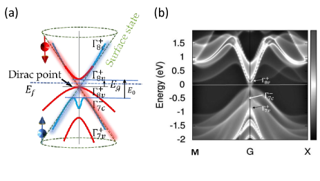
Major goals in current electronic devices are to increase the speed of electronic devices from the gigahertz to the terahertz range and to extend their functionalities by electron spin. [2] In these respects, topological insulators are promising materials for revolutionizing spintronics and other fields of emerging electronics.[3] The most remarkable properties of their helical surface states is spin-velocity locking that protects forbidden backscattering, ensures full spin polarization, the exceptional transport mobilities, and low energy dissipation, that is very attractive for semiconductor devices in high-speed communication applications. [2] The prerequisites of these properties is large spin polarization induced by means of surface currents. Illuminated by circularly polarized light, spin-polarized surface currents are excited via interband transitions between the occupied and unoccupied helical topological surface states restricted by angular momentum selection rule.[4, 5] Sn (gray tin) is the diamond-crystalline phase of elemental tin and a so-called “zero-gap semiconductor”.[6] Owing to its unusual band structure, extensive investigations were carried out primarily in the 1960s on bulk samples [7, 8, 9] and in the 1980s and 1990s on epitaxial films. [10, 11] More recently, the prediction and verification of Sn as a topological insulator (under strain) [12], has advantages over the established and experimentally confirmed binary () or ternary topological materials () that have the intrinsic problem of defect-induced bulk conductivity. Elemental tin, in contrast, is a much simpler system to be fabricated without a well-controlled composition requirement. It can be integrated into established compound semiconductor devices due to the substrate compatibility and quasi-lattice-matched to, for example, InSb (6.4798 Å).
Of primary interest for device applications is the recent observation of an optical transition in the infrared region at 0.41 eV () in Sn using spectroscopic ellipsometry that corresponds with a ‘negative’ band gap associated with an optical transition .[1] This interband optical transition could be asymmetric optical excitation from the occupied to the unoccupied states across the Dirac point in the helical Dirac cone, producing spin-polarized surface current. Therefore, understanding this transition has an important meaning for unprecedented applications. However the exact origin of this transition is not fully understood yet, calling for a renewed effort for a first-principles calculation of the optical properties which can be determined largely from its electronic band structure.
The band structure of Sn has many unusual features, including a degeneracy at the -point that closes the gap between the valence and conduction bands. Because of the strong relativistic Mass-Darwin effect on the -Sn in 5s electrons, the level moves down in the energy and dips below the level, resulting in band inversion. [13] Moreover, the strain and spin-orbit interaction influence the band structure considerably.[14] The band gap at the -point can be opened, however, through epitaxial strain or by alloying with Ge. In-plane compressive strain () in Sn grown on InSb substrate can lift the band degeneracy at the point creating a small band gap of 30 meV.[12] Careful consideration of many factors are needed to create an accurate fundamental model that manifests these several unusual features.
In this paper, we report the first-principles calculation of the band structure and optical properties of Sn. The emphasis is on the optical transition in the infrared region and the effect of the spin-orbit interaction and strain on the band structure and optical properties. Our calculations provide insight into the fundamental physics in the optical properties of -Sn in the infrared region.
II Methods
Density functional theory (DFT) has been applied as the standard method to investigate the properties of solids since it was initially proposed more than 50 years ago. It has been justified and validated that well-tuned pseudo-potentials can reproduce very precisely all-electron results for many properties of solids, but at a much lower computational time. By calculating the band gaps of a large data set of 473 solids with norm-conserving pseudopotentials and comparing with all-electron calculations, Borlido et. al. found the results are encouraging that on average, the absolute error is about 0.1 eV, yielding absolute relative errors in the 5-10 % range. [15] DFT and pseudo-potentials have been applied increasingly to study more complex system with techniques requiring massive computational efforts such as the many-body perturbation theory, spin-orbit interaction, and materials genome. [16]
To guarantee the accurate computational results using the exchange-correlation functionals, careful consideration and tests are essential to ensure the quality for simulating the properties of topological insulators.
To address the electronic and optical properties of topological insulators, two important factors need to be considered. The first is spin-orbit interaction. Topological surface states arise from spin-orbit interaction that is strong enough to change the band topology. [17] The second is many-body problem. In the DFT formalism, the ground state properties of a many-electron system are determined from the electron density distribution alone, which is described by a single determinant with all many-body effects included in one term, the exchange-correlation functional, avoiding massive computation of complex many-dimensional wave functions. [18] It is very important to validate and justify the appropriate the exchange-correlation functional describing the exchange correlation in many-electron systems.
All first-principles calculations are performed with the Vienna simulation package (VASP) (Version 5.4).[19] As mentioned above, the first-principles simulation results are sensitive to the exchang-correlation functionals chosen for a specific problem. To this end, the exchange-correlation is modeled with local density approximation (LDA) and hybrid functional (HSE). [20] We set the energy cutoff of the plane wave basis set to 500 eV. The frequency dependence of the dielectric function is calculated using the independent particle approximation provided within the VASP package. The -points are used in LDA calculation, while -points are used in HSE calculation using an averaging over multiple grids method. [21]
To incorporate strain into the band structure calculation, the deformation of the unit cell is set using the theory of linear elasticity. We explicitly calculate the experimentally relevant case of Sn grown epitaxially on an InSb (001) substrate. The lattice parameter of Sn and InSb is 6.4892 (20 ∘C ) [22] and 6.4794 (25 ∘C),[23] respectively. Due to the lattice mismatch, the InSb sublattice introduce in-plane compressive strain to the Sn film on the top of it. First-principles calculation is performed at 0 K. To simulate the strain effect, the volume of crystal is fixed by changing the ratio of lattice constant in the x-y axis, , and that in z axis, . The phase of Sn has the cubic diamond crystal structure with a lattice parameter of at 0 K estimated with LDA and estimated with HSE functional. Indeed, the band gap and optical property of a material can be sensitive to the lattice parameters. The electronic and optical properties of -Sn are calculated in such a way that the geometry optimization is performed with LDA approximation, which predicts the lattice parameter of -Sn, 6.4794 , with a reasonable error of -0.225% with respect to the experimental value, followed by a single point calculation of electronic and optical properties using using either the LDA or HSE funcationals.
When a film of Sn is coherently constrained to the InSb substrate lattice, it has a biaxial in-plane compressive strain, of , which is chosen to represent a reasonable strain effect and does not reflect the real value of the compressive strain because the linear thermal expansion fails when the temperature approaches 0 K. Thus, the corresponding lattice constant in the x-y axis . Assuming a linear elastic response, the out-of-plane strain is then , where GPa and GPa, [24] resulting in an out-of-plane lattice constant of .
It is worth mentioning that the deformation due to a bi-axially symmetric, in-plane strain is different from a uni-axial strain applied along the orthogonal direction. In the former case, ; in the latter case, . Our strain-dependent results should not be confused with calculations by others using different boundary conditions and definition of the compressive and tensile strain.[25, 26]
III Results
We discuss the first-principles calculation of the band structure Sn in section III.1 and its dielectric function in section III.2 focusing on the infrared transition and the influences of the spin-orbit interaction and in-plane compressive strain.
III.1 Electronic band structure of -Sn
The first-principles calculation are performed on -Sn to understand the relative influences of spin-orbit interaction and strain on electronic band structure of Sn regarding relative energy of bands. Of particular interest is the transition at 0.41 eV in our ellipsometric measurements. Previous experimental measurements typically cut-off above 1 eV [27]; Kufner . calculated the dielectric function of Sn using HSE hybrid functional, and compared the results with and without the spin-orbit interaction. The peak is not pronounced in the calculated dielectric function. [28] Pollak . calculated the band structure of Sn and assigned of 0.41 eV to the transition between . This transition has not been considered in any great detail.
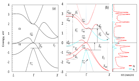
To understand the origin of the transition, we calculate the band structure with and without the spin-orbit interaction, and the density of states of Sn around the point, and present the results in Figure 1. The bands are labeled using the notation of Pollak et al. [9] and , superscripts denote the parity. Optical transitions are determined using selection rules, meaning transitions can only connect states with opposite parities.[29]
Without spin-orbit interaction, the transition occurs between and , which is lower than the valence band , demonstrating an inversed band structure shown in Figure 1 (a). The band structure (the position of light hole and heavy hole) of Sn is modified by spin-orbit interaction, shown in Figure 1 (b). subband is split from the valence band and band is shifted down by spin-orbit interaction.[12] This is caused by the quantum mechanical repulsion that the and band are pushed apart by the split-off band .[30]
Sn demonstrates the inverted band structure that the conduction band at the point is lower than the valence band , as shown in Figure 1 and 2. [7] The possible transitions are indicated in these Figures and listed in Table 1. In Figure 1(b), the band ordering calculated with LDA is , where is orbital character, and is a split-off valence band from which is mixed and orbital character, but is orbital character near the point shown in red line. is a conduction band of orbital character, which is lower than the valence band by 0.69 eV corresponding to interband transition.
The band gap calculated using LDA with and without the spin-orbit interaction is 0.70 eV and 0.28 eV, respectively. Without the spin-orbit interaction, the band gap estimated using the LDA is predicted correctly to be negative ( is lower than (), but is much lower than the experimental value 0.41 eV. That can be that the LDA underestimates the band gap due to the inaccurate description of the exchange correlation.[31] With the spin-orbit interaction, the is pushed down far to 0.70 eV, leading to an overestimated band inversion. LDA produces higher spin-orbit splitting,[32] it could be because a purely perturbative treatment of spin-orbit coupling is not sufficient in the LDA approximation. [33]
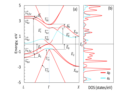
HSE has been applied to calculate the band gaps of covalent materials including semiconductors, [34] and has much more computational efficient than other many-body perturbation methods, and provides performances well in agreement with G0W0 or GW calculations.[31] With the spin-orbit interaction, HSE improved the band gap to 0.58 eV, better than LDA does, likely because incorporation of a fraction of the exchange within the HSE functional reduces self-interaction errors, leading to a better result. [35] The spin-orbit splitting is sensitive to the level of theory employed. As a result, the band order can be dependent on the exchange-correlation functional applied in the calculations. [35] The band order is calculated with HSE hybrid functional as shown in Figure 2, which is consistent with calculation, [9] but is different from the results obtained with LDA, where split-off band is higher than . transition occurs between and . Our value is 0.58 eV which is close to 0.52 eV reported in [13]. Both calculations using LDA and HSE hybrid functional show that the is interband transition between inverted the valence band and conduction band.
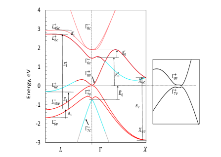
The calculated band structure of Sn under % biaxial compressive strain is presented in Figure 3 . The symmetry from the (cubic) unit cell to (tetragonal) caused by strain, see Figure S12 the supplementary material in [1]. The band structure in Figure 3 refers to the direction perpendicular to the plane of applied strain,i.e. the surface plane of the film.
The in-plane compressive strain changes the band structures. The most notable feature is that the strain opens a gap between the conduction band and valence band at the point, [36] as shown in the inlay in Figure 3. The magnitude of the gap opening depends on the computation method. The LDA functional gives 31 meV, which is closer to the value of 30 meV calculated under a in-plane compressive strain of % using QW quasi-particle calculation, [12] but larger than 13 meV calculated under the in-plane strain of using Pikus-Bir Hamiltonian.[1]
To gain insight into how the band structure changes with strain, we consider the general Luttiger Hamiltonian of an electron (or hole) in a semiconductor including only the four low-energy bands around the point.[37, 38]
The four low-energy bands of strained Sn around the point can be written as, [26]
| (1) |
where is an additional perturbation term created by externally applied strain and written as follows,
| (2) |
where is determined by the strength of the strain and for biaxial compressive strain.
Sn is an inverted band structure materials, where the light hole band moves up become unoccupied. Under the biaxial compressive strain, the light hole () band, , is pushed up (, and increases), while the heavy hole band, (), is pushed downward (, and decreases). A small gap thus opens between and under a in-plane compressive strain. This result quantitatively agrees with the computational and theoretical prediction, as shown in Figure 3.
The magnitudes of optical transitions such as , , and also are changed between 8.5 meV and 25 meV in Sn under in-plane compressive strain. This result is in consistent with the energy peaks estimated from the calculated dielectric function and our ellipsometry experiment discussed in III.2.
The strained -Sn is a topological elemental material, where the topological surface states are formed between and , as illustrated in Figure 8 in the appendix A. The direct interband transition in the topological surface states, from to the across the Dirac point, resulting in spin polarized photocurrents, which are very important for developing -Sn based spintronics.
III.2 Dielectric function of Sn
Once the band structure of -Sn is calculated, the frequency dependent dielectric function due to interband transitions can be calculation as follows. The imaginary part of the frequency dependent dielectric constant of -Sn, , is calculated within the independent-particle approximation and is expressed as, [39, 40, 41]
| (3) | |||||
where is the volume of the primitive cell, the Bloch vector of the incident wave, a wavevector within the first Brillouin zone, the indices c and v the conduction and the valence band states, respectively, the point weights, the unit vectors for the three Cartesian directions.
Subsequent calculation of the real part of the dielectric function, , is done by applying the Kramers-Kronig relationship.[41]
| (4) |
where denotes the principal value.
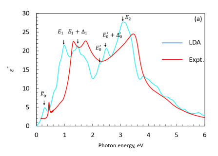
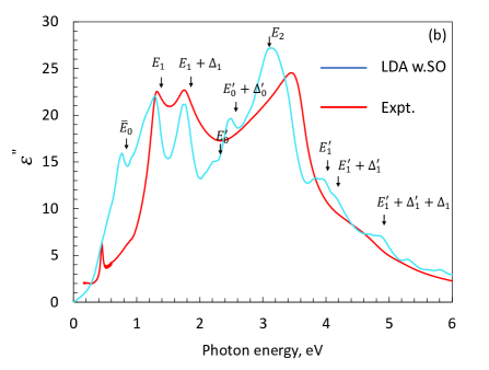
Since the imaginary part of the dielectric function is calculated based on the interband transitions, there is a good correlation between the energy peaks in the dielectric function and the interband transitions, making the assignment of energy peaks to the interband band transitions straightforward. [42] The main optical features are indicated by arrows and labeled with , …. being assigned to peaks according to the band gaps calculated in the electronic band structure in Figure 1 (a) without and with spin-orbit interaction. The energies of transitions in unstrained Sn shown in Figure 4 (a) and (b) are estimated using the method mentioned in [41] and are presented in Table 2, together with available experimental data.
The computed imaginary part of the frequency dependent dielectric function of Sn, without and with spin-orbit coupling calculated in the LDA scheme for exchange and correlation, are presented in Figure 4 (a) and 4 (b), respectively. In general, except for some deviations, the calculated imaginary part of dielectric functions agree well with the experimental measurement with respect to the line shape, peak positions, and peak intensities. [1] The following discussion is concentrated on the spin-orbit effect.
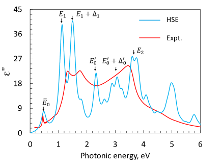
Figure 4 (b) shows that spin-orbit interaction has effects on of Sn, in particular, in lower energy region, in three respects. First, a finer lineshape is obtained. The calculated dielectric function captures transitions such as , , which are not clearly observed in the ellipsometric measurements shown in red line in Figure 4 (b). Second, calculated and peaks agreement better with the ellipsometric measurements. We calculated and to be 1.30 eV and 1.78 eV, close to our experimental value 1.278 eV and 1.73 eV, respectively.[1] But, The calculated value is higher than our experimental value by 0.35 eV. The calculated is 3.26 eV, lower than our experimental value by 0.19 eV.[1] Third, The magnitude of calculated peaks are comparable with these experimental values, with the largest difference in the peak, whose magnitude is three times higher than the value without spin-orbit interaction. These changes may be because, as we discussed earlier, split-off band modifies the band structure at point, where , , and transition occur (see calculated without and with spin-orbit interaction in Figure 1 (a) and (b), respectively). Moreover, the spin-orbit interaction induces the topological states, thus, altering the optical oscillator strength significantly by 20 % as compared to the normal system. [43] The oscillator strength of can be further strengthened by the hybridization of and orbits in and , as shown in Figure 1(b). Base on these facts, it can be concluded that energy peak is indeed from the interband transition between . [44] Nevertheless, there is no remarkable change in band structure at point, thus, peak is unchanged. The inclusion of spin-orbit interaction leads a better agreement with experimental measurement and the following discussion focuses on the results obtained from HSE functional. The dielectric function of Sn is also calculated using HSE functional with spin-orbit interaction and presented in Figure 5. The major difficulty of HSE functional is that the calculation is computationally demanding and slow to converge. To overcome the difficulty, the calculation is performed with improved dielectric method to moderate the number of points to accelerate converging. In consequence, the calculated dielectric function demonstrates wiggles and higher magnitude specifically and . Their positions are red-shift compared with experimental results and this seems to agree with the trend shown in Figure 4 (a). Peaks and demonstrate clearly. The estimated is 0.480 eV, which is close to our experimental value of 0.416 eV. Our result agrees with the argument that HSE is more appropriate for calculating optical gaps, in particular, for peak. [45] The significant difference in calculated value (representing the transition ) with LDA and HSE hybrid functional can be understood from the different band order of , , and near the point in the band structure, as shown in Figure 1 and 2, where LDA overestimates the spin-orbit interaction as discussed before. LDA can predict the dielectric function of -Sn with a good agreement with the experimental measurement, except overestimating the peak by 0.36 eV. In contrast, HSE captures the peak precisely, but underestimates the and by 0.15 and 0.24 eV, respectively.
| Energies | This work | Exp. 111The experimental data from Ref. [1] | Exp. 222The experimental data from Ref. [8] | ||
|---|---|---|---|---|---|
| LDA (w.SO) | LDA | HSE | |||
| 0.769 | 0.30 | 0.480 | 0.410 | ||
| 1.30 | 1.00 | 1.129 | 1.278 | 1.365 | |
| 1.78 | 1.48 | 1.489 | 1.73 | 1.845 | |
| 3.26 | 3.10 | 3.602 | 3.45 | 3.718 | |
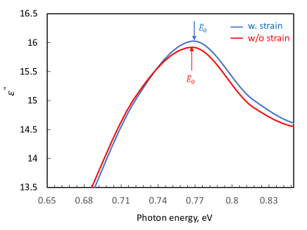
The dielectric function of Sn around with % in-plane compressive strain is calculated and presented together with results without strain in Figure 6. The strain increases slightly the peak by 1.5 meV, which agrees with our recent ellipsometric measurement that showed critical points by 5 meV by in-plain strain of using deformation formalism.[1] More importantly, it provides evidence that the transition does not arise from externally applied strain, but instead from a direct interband transition .
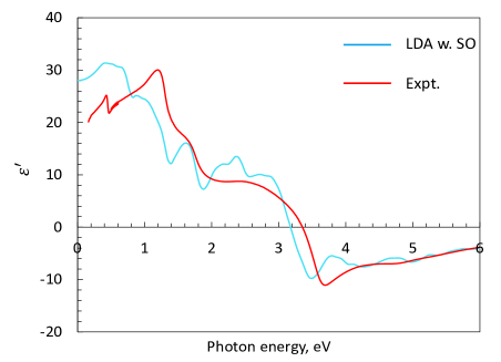
The real part of the dielectric function is shown in Figure 7 along with the experimentally determined . A sum rule [29] is used to estimate as 23.4, [1] which is close to measured by infrared polarized reflectance. [46] The calculated dielectric constant is 28, which is larger than the experimental value by 4. The becomes negative at 3.2 eV and continue to the minimum point at 3.45 eV, which relates to transition. The other optical properties of -Sn, such as refractive index and absorption spectrum, which are mainly naturally derived from the dielectric constants are presented in the appendix B and C, respectively for reference.
IV Conclusion
In this paper, we explore the dielectric function of Sn both unstained and strained with a focus on the infrared wavelength (photon energy 1 eV) using the first-principles method. The optical transition at 0.41 eV observed in the our elliposometric experiment originates from the interband transition and is explained by combining first-principles calculation of the band structure and dielectric function. In the strained Sn, this asymmetric optical excitation from the occupied to the unoccupied states across the Dirac point in the helical Dirac cone, producing spin-polarized surface current. This conclusion could provide a foundation for further study of the spin-polarized photocurrent in strained Sn, a topological elemental material, and for its applications in high-speed communications and opto-electronic devices. Validation and justification of the exchange-correlation functionals are very important in calculation of the electronic and optical properties of the topological materials. HSE can capture the interband excitation in the helical Dirac cone with a reasonable accuracy, but LDA overestimates this transition.
Appendix A Topological surface states in strained -Sn
The helical surface states in -Sn are calculated with HSE and shown in Figure 8. The optical transition across the Dirac point, which is below the Fermi level, in the helical Dirac cone.
Appendix B The refractive index of -Sn
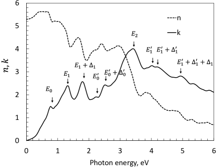
The refractive index () and extinction coefficient () is calculated for -Sn using the following equations [47] and demonstrated in Figure 9.
| (5) |
| (6) |
where and are taken from the dielectric function computed using LDA with inclusion of spin orbit interaction, as discussed in section III.2. The extinction coefficient demonstrates distinct peaks associated with transitions, which are labeled in Figure 9. For example, the peak at 0.71 eV corresponds to transition.
Appendix C The absorption spectrum of -Sn
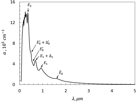
The absorption coefficient is calculated using a relation: [47]
| (7) |
where is the extinction coefficient obtained with equation 6 in section C, is the wavelength. The calculated absorption spectrum of -Sn is shown in Figure 10.
The absorption spectrum captures the critical points in the long wavelength region. In particular, the absorption peak at 1.614 corresponds to transition ( to ). Transitions , , and also the transitions due to spin orbit spiting, , ′, , are clearly obvious.
The absorption spectrum of -Sn also provide the information of the band structure. -Sn becomes a direct band gap semiconductor in the long wavelength region because an absorption peak at 1.614 is observed. The transition and are indirect because both conduction and valence band edges are not at the center of the Brillouin zone.
Acknowledgements.
J. S. D. wishes to thank Air Force Office of Scientific Research for financial support and DoD High Performance Computing Modernized Program for providing computational support.References
- Carrasco et al. [2018] R. A. Carrasco, C. M. Zamarripa, S. Zollner, J. Menéndez, S. A. Chastang, J. Duan, G. J. Grzybowski, B. B. Claflin, and A. M. Kiefer, The direct bandgap of gray -tin investigated by infrared ellipsometry, Applied Physics Letters 113, 232104 (2018).
- Braun et al. [2016] L. Braun, G. Mussler, A. Hruban, M. Konczykowski, T. Schumann, M. Wolf, M. Münzenberg, L. Perfetti, and T. Kampfrath, Ultrafast photocurrents at the surface of the three-dimensional topological insulator bi2se3, Nature communications 7, 1 (2016).
- Gladczuk et al. [2021] Ł. Gladczuk, L. Gladczuk, P. Dluzewski, G. van der Laan, and T. Hesjedal, Study of spin pumping through -sn thin films, physica status solidi (RRL)–Rapid Research Letters 15, 2100137 (2021).
- McIver et al. [2012] J. McIver, D. Hsieh, H. Steinberg, P. Jarillo-Herrero, and N. Gedik, Control over topological insulator photocurrents with light polarization, Nature nanotechnology 7, 96 (2012).
- Bai et al. [2022] Y. Bai, N. Li, R. Li, and P. Liu, Ultrafast dynamics of helical dirac fermions in the topological insulators, Advances in Physics: X 7, 2013134 (2022).
- Ewald and Tufte [1958] A. Ewald and O. Tufte, Gray tin single crystals, Journal of Applied Physics 29, 1007 (1958).
- Groves and Paul [1963] S. Groves and W. Paul, Band structure of gray tin, Physical Review Letters 11, 194 (1963).
- Cardona et al. [1966] M. Cardona, P. McElroy, F. H. Pollak, and K. L. Shaklee, Electroreflectance and band structure of gray tin, Solid State Communications 4, 319 (1966).
- Pollak et al. [1970] F. H. Pollak, M. Cardona, C. Higginbotham, F. Herman, and J. P. Van Dyke, Energy-band structure and optical spectrum of grey tin, Physical Review B 2, 352 (1970).
- Tu et al. [1989] L.-W. Tu, G. K. Wong, and J. B. Ketterson, Growth of n-type heteroepitaxial films of gray tin on (001) cdte by molecular beam epitaxy, Applied physics letters 54, 1010 (1989).
- John et al. [1989] P. John, T. Miller, and T.-C. Chiang, Core-level photoemission studies of the -sn/insb (100) heterostructure system, Physical Review B 39, 3223 (1989).
- Barfuss et al. [2013] A. Barfuss, L. Dudy, M. R. Scholz, H. Roth, P. Höpfner, C. Blumenstein, G. Landolt, J. Dil, N. Plumb, M. Radovic, et al., Elemental topological insulator with tunable fermi level: Strained -sn on insb (001), Physical Review Letters 111, 157205 (2013).
- Küfner et al. [2013a] S. Küfner, J. Furthmüller, L. Matthes, M. Fitzner, and F. Bechstedt, Structural and electronic properties of -tin nanocrystals from first principles, Physical Review B 87, 235307 (2013a).
- Reno and Stephenson [1990] J. Reno and L. Stephenson, The stability of -sn grown on cdte by molecular beam epitaxy, Journal of electronic materials 19, 549 (1990).
- Borlido et al. [2020] P. Borlido, J. Doumont, F. Tran, M. A. Marques, and S. Botti, Validation of pseudopotential calculations for the electronic band gap of solids, Journal of chemical theory and computation 16, 3620 (2020).
- Kucukbenli et al. [2014] E. Kucukbenli, M. Monni, B. Adetunji, X. Ge, G. Adebayo, N. Marzari, S. De Gironcoli, and A. D. Corso, Projector augmented-wave and all-electron calculations across the periodic table: a comparison of structural and energetic properties, arXiv preprint arXiv:1404.3015 (2014).
- Che et al. [2020] X. Che, Q. Pan, B. Vareskic, J. Zou, L. Pan, P. Zhang, G. Yin, H. Wu, Q. Shao, P. Deng, et al., Strongly surface state carrier-dependent spin–orbit torque in magnetic topological insulators, Advanced Materials 32, 1907661 (2020).
- Flores et al. [2018] M. A. Flores, W. Orellana, and E. Menéndez-Proupin, Accuracy of the heyd-scuseria-ernzerhof hybrid functional to describe many-electron interactions and charge localization in semiconductors, Physical Review B 98, 155131 (2018).
- Kresse and Furthmuller [2001] G. Kresse and J. Furthmuller, Vienna ab-initio simulation package (vasp), Vienna: Vienna University (2001).
- Blöchl [1994] P. E. Blöchl, Projector augmented-wave method, Physical review B 50, 17953 (1994).
- Bokdam et al. [2016] M. Bokdam, T. Sander, A. Stroppa, S. Picozzi, D. Sarma, C. Franchini, and G. Kresse, Role of polar phonons in the photo excited state of metal halide perovskites, Scientific reports 6, 1 (2016).
- Oehme et al. [2011] M. Oehme, J. Werner, M. Gollhofer, M. Schmid, M. Kaschel, E. Kasper, and J. Schulze, Room-temperature electroluminescence from gesn light-emitting pin diodes on si, IEEE Photonics Technology Letters 23, 1751 (2011).
- Straumanis and Kim [1965] M. Straumanis and C. Kim, Lattice parameters, thermal expansion coefficients, phase width, and perfection of the structure of gasb and insb, Journal of Applied Physics 36, 3822 (1965).
- Moontragoon et al. [2007] P. Moontragoon, Z. Ikonić, and P. Harrison, Band structure calculations of si–ge–sn alloys: achieving direct band gap materials, Semiconductor science and technology 22, 742 (2007).
- Hinckley and Singh [1990] J. Hinckley and J. Singh, Influence of substrate composition and crystallographic orientation on the band structure of pseudomorphic si-ge alloy films, Physical review B 42, 3546 (1990).
- Ruan et al. [2016] J. Ruan, S.-K. Jian, H. Yao, H. Zhang, S.-C. Zhang, and D. Xing, Symmetry-protected ideal weyl semimetal in hgte-class materials, Nature communications 7, 1 (2016).
- Vina et al. [1984] L. Vina, S. Logothetidis, and M. Cardona, Temperature dependence of the dielectric function of germanium, Physical Review B 30, 1979 (1984).
- Küfner et al. [2013b] S. Küfner, J. Furthmüller, L. Matthes, and F. Bechstedt, Optical absorption and emission of -sn nanocrystals from first principles, Nanotechnology 24, 405702 (2013b).
- Peter and Cardona [2010] Y. Peter and M. Cardona, Fundamentals of semiconductors: physics and materials properties (Springer Science & Business Media, 2010).
- Chao and Chuang [1992] C. Y.-P. Chao and S. L. Chuang, Spin-orbit-coupling effects on the valence-band structure of strained semiconductor quantum wells, Physical Review B 46, 4110 (1992).
- Giovannetti et al. [2015] G. Giovannetti, M. Capone, J. van den Brink, and C. Ortix, Kekulé textures, pseudospin-one dirac cones, and quadratic band crossings in a graphene-hexagonal indium chalcogenide bilayer, Physical Review B 91, 121417 (2015).
- Scherpelz et al. [2016] P. Scherpelz, M. Govoni, I. Hamada, and G. Galli, Implementation and validation of fully relativistic gw calculations: spin–orbit coupling in molecules, nanocrystals, and solids, Journal of chemical theory and computation 12, 3523 (2016).
- Sakuma et al. [2011] R. Sakuma, C. Friedrich, T. Miyake, S. Blügel, and F. Aryasetiawan, G w calculations including spin-orbit coupling: Application to hg chalcogenides, Physical Review B 84, 085144 (2011).
- Janesko et al. [2009] B. G. Janesko, T. M. Henderson, and G. E. Scuseria, Screened hybrid density functionals for solid-state chemistry and physics, Physical Chemistry Chemical Physics 11, 443 (2009).
- Ramasubramaniam [2012] A. Ramasubramaniam, Large excitonic effects in monolayers of molybdenum and tungsten dichalcogenides, Physical Review B 86, 115409 (2012).
- Yang et al. [2004] L. Yang, J. R. Watling, R. C. Wilkins, M. Borici, J. R. Barker, A. Asenov, and S. Roy, Si/sige heterostructure parameters for device simulations, Semiconductor Science and Technology 19, 1174 (2004).
- Luttinger [1956] J. M. Luttinger, Quantum theory of cyclotron resonance in semiconductors: General theory, Physical review 102, 1030 (1956).
- Zhang et al. [2018] D. Zhang, H. Wang, J. Ruan, G. Yao, and H. Zhang, Engineering topological phases in the luttinger semimetal -sn, Physical Review B 97, 195139 (2018).
- Adolph et al. [1996] B. Adolph, V. Gavrilenko, K. Tenelsen, F. Bechstedt, and R. Del Sole, Nonlocality and many-body effects in the optical properties of semiconductors, Physical Review B 53, 9797 (1996).
- Grosso and Parravicini [2000] G. Grosso and G. P. Parravicini, Optical and transport properties in metals, Solid State Physics , 396 (2000).
- Gajdoš et al. [2006] M. Gajdoš, K. Hummer, G. Kresse, J. Furthmüller, and F. Bechstedt, Linear optical properties in the projector-augmented wave methodology, Physical Review B 73, 045112 (2006).
- Albanesi et al. [2000] E. A. Albanesi, C. Okoye, C. O. Rodríguez, E. P. y Blanca, and A. Petukhov, Electronic structure, structural properties, and dielectric functions of iv-vi semiconductors: Pbse and pbte, Physical Review B 61, 16589 (2000).
- Díaz-Fernández et al. [2018] A. Díaz-Fernández, N. del Valle, E. Díaz, and F. Domínguez-Adame, Topologically protected states in -doped junctions with band inversion, Physical Review B 98, 085424 (2018).
- Lu et al. [2019] X. Lu, X. Li, and L. Yang, Modulated interlayer exciton properties in a two-dimensional moiré crystal, Physical Review B 100, 155416 (2019).
- Brothers et al. [2008] E. N. Brothers, A. F. Izmaylov, J. O. Normand, V. Barone, and G. E. Scuseria, Accurate solid-state band gaps via screened hybrid electronic structure calculations, The Journal of chemical physics 129, 011102 (2008).
- Lindquist and Ewald [1964] R. E. Lindquist and A. Ewald, Optical constants of single-crystal gray tin in the infrared, Physical Review 135, A191 (1964).
- Adachi [1989] S. Adachi, Optical properties of -sn, Journal of applied physics 66, 813 (1989).
- Tong et al. [2020] C.-J. Tong, H. J. Edwards, T. D. Hobson, K. Durose, V. R. Dhanak, J. D. Major, and K. P. McKenna, Density functional theory and experimental determination of band gaps and lattice parameters in kesterite cu2znsn (s x se1–x) 4, The journal of physical chemistry letters 11, 10463 (2020).
- Batista et al. [2006] E. R. Batista, J. Heyd, R. G. Hennig, B. P. Uberuaga, R. L. Martin, G. E. Scuseria, C. Umrigar, and J. W. Wilkins, Comparison of screened hybrid density functional theory to diffusion monte carlo in calculations of total energies of silicon phases and defects, Physical Review B 74, 121102 (2006).
- Zhang et al. [2013] D. Zhang, W. Lou, M. Miao, S.-c. Zhang, and K. Chang, Interface-induced topological insulator transition in gaas/ge/gaas quantum wells, Physical review letters 111, 156402 (2013).
- Kastl et al. [2015] C. Kastl, C. Karnetzky, H. Karl, and A. W. Holleitner, Ultrafast helicity control of surface currents in topological insulators with near-unity fidelity, Nature communications 6, 1 (2015).
- Matsushita et al. [2011] Y.-i. Matsushita, K. Nakamura, and A. Oshiyama, Comparative study of hybrid functionals applied to structural and electronic properties of semiconductors and insulators, Physical Review B 84, 075205 (2011).
- Yakovkin and Dowben [2007] I. Yakovkin and P. Dowben, The problem of the band gap in lda calculations, Surface Review and Letters 14, 481 (2007).
- Brivio et al. [2014] F. Brivio, K. T. Butler, A. Walsh, and M. Van Schilfgaarde, Relativistic quasiparticle self-consistent electronic structure of hybrid halide perovskite photovoltaic absorbers, Physical Review B 89, 155204 (2014).
- Zollner et al. [2000] S. Zollner, A. Demkov, R. Liu, P. Fejes, R. Gregory, P. Alluri, J. Curless, Z. Yu, J. Ramdani, R. Droopad, et al., Optical properties of bulk and thin-film srtio 3 on si and pt, Journal of Vacuum Science & Technology B: Microelectronics and Nanometer Structures Processing, Measurement, and Phenomena 18, 2242 (2000).
- Alouani and Wills [1996] M. Alouani and J. Wills, Calculated optical properties of si, ge, and gaas under hydrostatic pressure, Physical Review B 54, 2480 (1996).
- Nguyen et al. [2020] H. T. Nguyen, V. L. Le, T. M. H. Nguyen, T. J. Kim, X. A. Nguyen, B. Kim, K. Kim, W. Lee, S. Cho, and Y. D. Kim, Temperature dependence of the dielectric function and critical points of -sns from 27 to 350 k, Scientific reports 10, 1 (2020).
- Rhim et al. [2005] S. Rhim, M. Kim, A. J. Freeman, and R. Asahi, Fully first-principles screened-exchange lda calculations of excited states and optical properties of iii-v semiconductors, Physical Review B 71, 045202 (2005).
- Kootstra et al. [2000] F. Kootstra, P. De Boeij, and J. Snijders, Application of time-dependent density-functional theory to the dielectric function of various nonmetallic crystals, Physical Review B 62, 7071 (2000).
- Sun et al. [2006] J. Sun, X.-F. Zhou, Y.-X. Fan, J. Chen, H.-T. Wang, X. Guo, J. He, and Y. Tian, First-principles study of electronic structure and optical properties of heterodiamond bc 2 n, Physical Review B 73, 045108 (2006).
- Filip et al. [2013] M. R. Filip, C. E. Patrick, and F. Giustino, G w quasiparticle band structures of stibnite, antimonselite, bismuthinite, and guanajuatite, Physical Review B 87, 205125 (2013).
- Dal Corso and Conte [2005] A. Dal Corso and A. M. Conte, Spin-orbit coupling with ultrasoft pseudopotentials: Application to au and pt, Physical Review B 71, 115106 (2005).
- Fuchs et al. [2002] M. Fuchs, J. L. F. Da Silva, C. Stampfl, J. Neugebauer, and M. Scheffler, Cohesive properties of group-iii nitrides: A comparative study of all-electron and pseudopotential calculations using the generalized gradient approximation, Physical Review B 65, 245212 (2002).
- Jenkins et al. [2016] G. Jenkins, C. Lane, B. Barbiellini, A. Sushkov, R. Carey, F. Liu, J. Krizan, S. Kushwaha, Q. Gibson, T.-R. Chang, et al., Three-dimensional dirac cone carrier dynamics in na 3 bi and cd 3 as 2, Physical Review B 94, 085121 (2016).
- Conte et al. [2017] A. M. Conte, O. Pulci, and F. Bechstedt, Electronic and optical properties of topological semimetal cd3as2, Scientific Reports 7 (2017).
- Liu et al. [2022] S. Liu, A. C. Covian, J. A. Gardener, A. Akey, B. D. Levin, X. Wang, and J. Liu, Growth of -sn on silicon by a reversed -sn to -sn phase transformation for quantum material integration, Communications Materials 3, 1 (2022).
- Fu et al. [2007] L. Fu, C. L. Kane, and E. J. Mele, Topological insulators in three dimensions, Physical review letters 98, 106803 (2007).
- Hummer et al. [2009] K. Hummer, J. Harl, and G. Kresse, Heyd-scuseria-ernzerhof hybrid functional for calculating the lattice dynamics of semiconductors, Physical Review B 80, 115205 (2009).