Combined Spectroscopy and Electrical Characterization of La:BaSnO
Thin Films and Heterostructures
Abstract
For La-doped BaSnO thin films grown by pulsed laser deposition, we combine chemical surface characterization and electronic transport studies to probe the evolution of electronic states in the band structure for different La-doping content. Systematic analyses of spectroscopic data based on fitting the core electron line shapes help to unravel the composition of the surface as well as the dynamics associated with increasing doping. This dynamics is observed with a more pronounced signature in the Sn 3d core level, which exhibits an increasing asymmetry to the high binding energy side of the peak with increasing electron density. The present results expand the current understanding of the interplay between the doping concentration, electronic band structure and transport properties of epitaxial La:BaSnO films.
The perovskite La-doped BaSnO (La:BaSnO) is a novel transparent oxide semiconductor that exhibits outstanding room temperature (RT) electron mobility () with high carrier density together with a high optical transmittance [1, 2, 3]. Owing to its unique electronic and optical properties, La:BaSnO has the potential for applications in transparent electronics [4, 5, 6, 7], photovoltaics [8, 9, 10, 11], as well as in thermoelectric [12, 13, 14, 15] and multifunctional perovskite-based optoelectronic devices [16, 17, 10]. Furthermore, its low-power consumption combined with its ability to be heavily doped and its good stability at high temperatures make La:BaSnO a suitable material for integration in thermally stable capacitors, field effect transistors and power electronic devices [18, 3, 19, 17, 4].
The discovery of a RT of (with corresponding carrier density, ) in La:BaSnO single crystals [1, 2, 3] stimulated intense investigation into this material [4]. Particularly, the potential of La:BaSnO for device applications and heterostructures triggered considerable interest in thin films grown from this compound [17, 5, 20, 21, 22, 15, 23, 24, 25, 26, 27, 28, 29, 30, 7, 6, 31, 19, 32, 33, 7, 34, 35, 36, 37, 34, 38]. However, the reported in La:BaSnO thin films have only reached a maximum value of () for epitaxial films grown by molecular beam epitaxy (MBE) [33]. Other growth techniques resulted in the following electron mobilities: () for pulsed laser deposition (PLD) [27], () for high-pressure magnetron sputtering [36], and () for chemical solution deposition [39]. Various strategies to improve the mobility in La:BaSnO epitaxial films have been explored. Such efforts include, for example, incorporation of undoped BaSnO buffer layers to compensate for the lattice mismatch between the substrate and the active La:BaSnO top layers [7, 19, 26, 33], adsorption-controlled MBE for improved stoichiometry control [33, 40, 31, 32], a very high-temperature grown insulating buffer layer to reduce the density of threading dislocations [27], and post growth annealing processes [24, 22, 41]. Besides the ongoing efforts for RT improvement, in order to gain a better understanding of the conduction mechanisms in La:BaSnO films, it is important to establish a proper correlation between the transport characteristics and the behavior of the electronic states in the conduction band. This is crucial because the high ambient in La:BaSnO has been proposed to originate from both the small effective mass of the electrons at the conduction band minimum (CBM) [25, 42], which is associated with the largely dispersive Sn 5s conduction band, and the low optical phonon scattering rate [19, 43].
Although several studies used photoemission spectroscopy techniques to investigate the electronic structure of La:BaSnO films [44, 45, 43, 32, 46], only a few reports have combined electronic transport and spectroscopic studies to explore the evolution of electronic states in La:BaSnO films and heterostructures at different La-doping levels [43, 32]. In particular, recent ex-situ hard x-ray photoemission spectroscopy (HAXPES) experiments on La:BaSnO films demonstrated that both the CBM and the valence band maximum (VBM), as well as the core electrons are effectively modified with increasing carrier density [32]. Thus, this result calls for additional combined spectroscopic and electrical characterizations to facilitate more quantitative exploration of the evolution of the intrinsic properties of La:BaSnO films and heterostructures at different doping levels.
In the present paper we combine chemical surface analysis as a function of La doping using x-ray photoelectron spectroscopy (XPS) and electronic transport studies to explore the evolution of the electronic states in La:BaSnO films and heterostructures. From the transport measurements, we extract the transport characteristics, as well as and of the La:BaSnO samples. The surface properties of these samples are subsequently investigated using spectroscopic techniques. A direct connection between the electronic transport characteristics and the spectroscopic data is demonstrated. We used XPS as a probing tool to measure the changes in the films spectra associated with the increasing amount of La dopant. Through the analysis and systematic fits of the core XPS spectra, we are able to extract the binding energy values of the constituent elements along with the associated oxidation states. These data are consistent with the electron energy loss spectroscopy (EELS) data, as well as with the literature. By increasing the doping concentration, we observe shifts of the valence band leading edges toward higher binding energies, as well as increases in the states in the conduction band. More importantly, we provide a quantitative understanding of the effect of conduction band filling in La:BaSnO films and heterostructures. This effect is manifested by an increasing asymmetry in the line shape of the Sn 3d core spectra and leads to considering an additional plasmon satellite peak in the analysis of Sn 3d spectra.
| Sample name | Sample layout | Carrier density | Carrier mobility |
|---|---|---|---|
| ( cm) | (cm V s) | ||
| A | 6% La:BaSnO (25 nm)/BaSnO (100 nm)/DyScO | ||
| B | 6% La:BaSnO (25 nm)/BaSnO (100 nm)/TbScO | ||
| C | 6% La:BaSnO (25 nm)/SrTiO | ||
| D | 2% La:BaSnO (25 nm)/TbScO | ||
| E | 4% La:BaSnO (100 nm)/BaSnO (25 nm)/SrTiO |
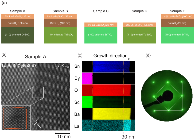
Epitaxial La:BaSnO films and heterostructures (samples labeled A to E in Table 1) were prepared by PLD ( nm). Prior to deposition, the (100) oriented SrTiO, (110) oriented DyScO and TbScO crystalline substrates were terminated in situ at 1300°C using a CO2 laser substrate heating system [47]. Figure 1(a) depicts a schematic view of the sample types investigated. The films were grown from La:BaSnO3 targets of 2%, 4% and 6% La doping contents. Details about the growth and systematic characterization of the films are provided in Ref. [27] [see details on the PLD growth conditions in Table S1 of the supplemental information].
Electrical transport properties were measured in a physical property measurement system (PPMS) in a van der Pauw geometry obtained by wire bonding aluminum wires to the samples’ corners [see Fig. S1(a) of the supplementary information]. The carrier concentration, , and the electron mobility, , were determined following the procedure discussed elsewhere [27, 48, 49, 50]. Table 1 gives the carrier density and electron mobility of the different sample types investigated in this study. The La:BaSnO samples analyzed here in both spectroscopy and transport experiments have a RT carrier concentration ranging from to ; and carrier mobility from to . The measured carrier densities reported are smaller than the expected values associated with the nominal concentration of the La dopant. In fact, the doping levels corresponding to 2%, 4% and 6% La are cm, cm and cm, respectively. The observed discrepancy can be ascribed to the high density of dislocation defects present in the films, as seen in the weak beam dark field scanning transmission electron microscopy micrographs [Fig. S1(b)-(d)]. These defects arise because the films are grown on substrates to which they are poorly lattice matched; and this often results in the reduction of the carrier density and electron mobility in epitaxial La:BaSnO3 films [27, 33, 31, 2] [see more details in section S1 of the supplemental information].
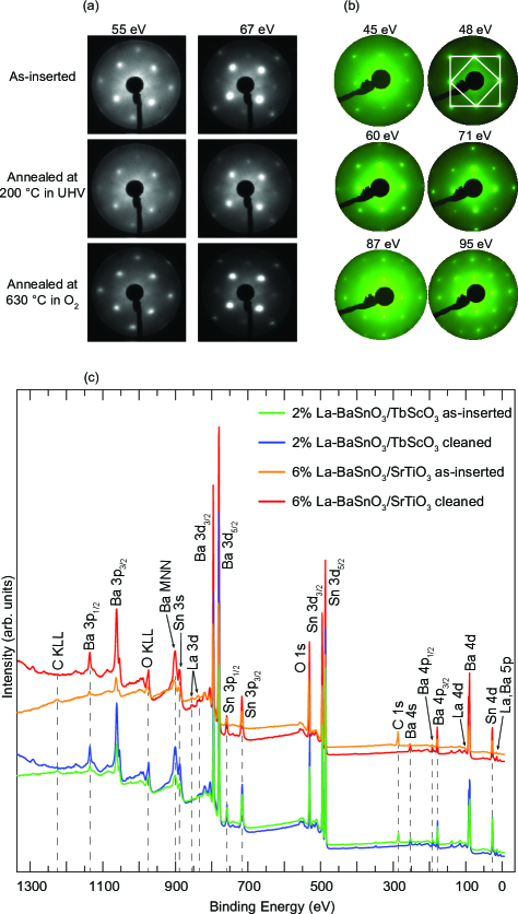
Following the procedure described in Ref. [51], the samples were systematically cleaned in ultra-high vacuum (UHV) before photoemission experiments. The surface structure of the samples was characterized using low-energy electron diffraction (LEED) [see Fig. S2(a)-(b) in supplementary information]. The surface of the clean La:BaSnO3 surface showed a stable 11 surface structure [Fig. 1(d)]. The diffraction spots form square lattices in reciprocal space corresponding to the cubic lattice structure of BaSnO in real space, thus indicating the high crystallinity of the films [52]. The cleanliness of the samples was checked by monitoring the LEED patterns directly after an annealing cycle, and also by comparing the XPS survey scans before and after cleaning [see Fig. S2 in supplementary information].
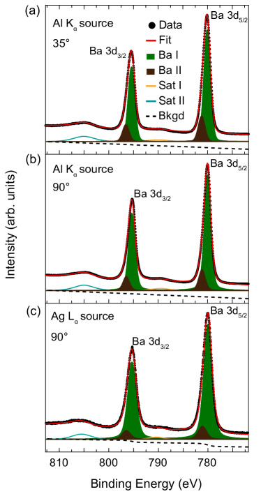
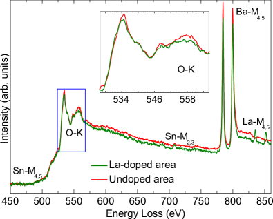
Figure 1(b) shows a representative scanning transmission electron microscopy (STEM) image of the investigated La:BaSnO heterostructure (sample A). To investigate the stoichiometry and evaluate the composition of the epitaxial layers, EELS measurements were performed on the cross section of the samples during STEM characterization. Figure 1(c) displays a representative EELS elemental mapping (atomic layer distribution) of the sample A for a total layer thickness of 120 nm of which the La-doped layer is 25 nm thick. The black color suggests a zero intensity, whereas the other colors indicate the presence of different elements (La, Ba, Sn, Dy, Sc, O) that are resolved in the scanned region. The elemental composition of the different layers of the La:BaSnO/BaSnO heterostructure is also evidenced in the EELS spectra for the same sample presented in Fig. 2. Looking at all the ionized edges, it can be seen that the spectra of the BaSnO (red curve) and La:BaSnO (green curve) are very similar, apart from the transfer of spectral weight to the La peaks in the latter. This spectral weight transfer is illustrated by the reduction of the intensity at the Ba-M edge. Intensity reduction is also noticeable at the O-K edge, and could well be due to electronic (charge) modulation associated with the substitution of the bivalent Ba2+ atoms with the trivalent La3+ ones [53]. Furthermore, the line shape of the spectra around the O-K feature [see inset Fig. 2] indicate good stoichiometry (no oxygen deficiency) in bulk layers, since these are in good agreement with the O-K EELS spectra reported for stoichiometric BaSnO and La:BaSnO films [33, 54, 55].
| Sample name | Ba | Sn | O |
|---|---|---|---|
| B | 20% | 16% | 64% |
| C | 25% | 15% | 60% |
| D | 22% | 16% | 62% |
| E | 23% | 13% | 64% |
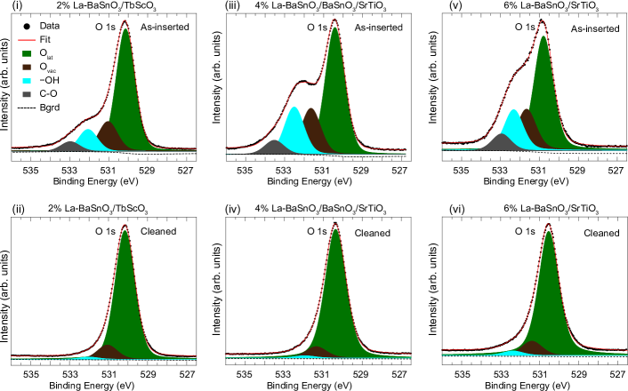
Table 2 presents the elemental composition of the surface of the films obtained from the fit of the XPS spectra. The composition is consistent throughout the surface of the various samples, with a larger proportion of Ba compared to Sn. Most importantly, the oxygen proportion in these high temperature annealed samples demonstrates the stability of the oxygen atoms in La:BaSnO [1, 3], and highlights the robustness of the sample cleaning procedure.
| Peak | Peak | Relative | FWHM | |
|---|---|---|---|---|
| assignment | position | intensity | ||
| () | () | () | ||
| 35 | Ba I | 780.08 | 82 | 1.58 |
| Al anode | Ba II | 781.21 | 18 | 1.58 |
| 90 | Ba I | 780.00 | 85 | 1.53 |
| Al anode | Ba II | 781.13 | 15 | 1.53 |
| 90 | Ba I | 780.00 | 90 | 1.97 |
| Ag anode | Ba II | 781.13 | 10 | 1.97 |
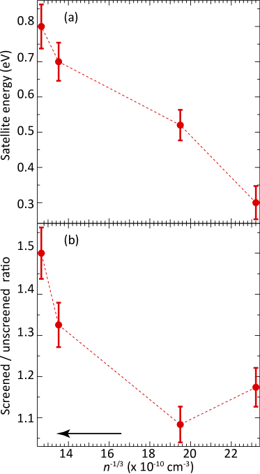
| Sample name | Peak assignment | Peak position | FWHM | Relative intensity | Satellite energy | Carrier density |
|---|---|---|---|---|---|---|
| () | () | () | (eV) | ( cm) | ||
| E | Screened | 486.76 | 1.07 | 54 | 0.30 | |
| Unscreened | 487.06 | 1.66 | 46 | |||
| D | Screened | 486.51 | 1.15 | 52 | 0.52 | |
| Unscreened | 487.03 | 1.34 | 48 | |||
| C | Screened | 486.80 | 1.06 | 57 | 0.70 | |
| Unscreened | 487.50 | 1.34 | 43 | |||
| B | Screened | 486.75 | 1.12 | 60 | 0.80 | |
| Unscreened | 487.55 | 1.40 | 40 |
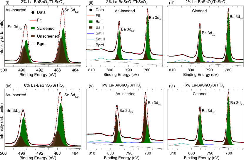
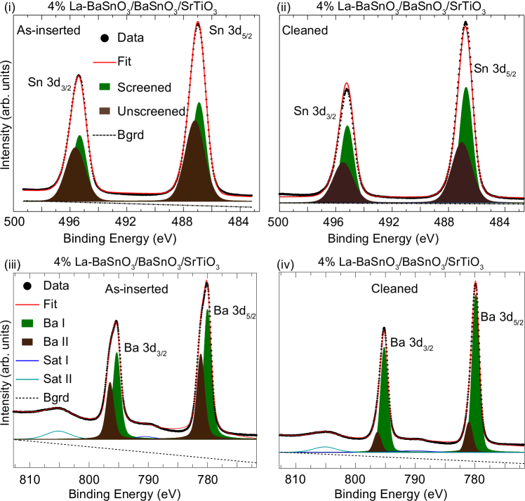
Figure 3 represents the XPS spectra of the Ba 3d core electrons together with the Voigt function fits. The Ba 3d spectra of all the samples showed an asymmetric line shape, suggesting the presence of multiple components in the core level. Two symmetric Voigt doublets (Ba I and Ba II) were used to fit the spectra. The main doublet, Ba I, located at the binding energy of 780.00 eV, is assigned to lattice barium in the Ba state, consistent with previous spectroscopic results on powder and epitaxial thin films of BaSnO [56, 57]. The second doublet, Ba II, situated at higher binding energy (781.13 eV), has been attributed to a surface character in several reports on epitaxial BaTiO films [58, 59, 60]. This component was suggested to originate either from under-coordinated barium at a BaO terminated surface, or from lattice relaxation [59, 60].
In comparing the XPS spectra for cleaned surfaces with those of surfaces measured as-inserted [see Figs. S3 and S4 of the supplemental information], the relative intensity of Ba II was observed to decrease after the treatment of the surfaces, while that of Ba I increases. This trend suggests that Ba II could be a surface component, which is amplified with contamination. The nature of the Ba II peak was carefully investigated by carrying out a systematic analysis of its fraction with respect to the probing depth. This was achieved by performing angle-dependent XPS measurements as depicted in Fig. 3. The measurements were first performed using the Al Kα anode (photon energy of 1486.71 eV) at electron take-off angles of 35 [Fig. 3(a)] and 90 (normal emission) [Fig. 3(b)], and later the excitation source was changed to Ag Lα anode (photon energy of 2984.31 eV) for acquisition at normal emission [Fig. 3(c)]. For the take-off angle of 35, the photoelectrons emitted originate from a region nearer the surface, whereas at the take-off angle of 90, the emitted photoelectrons are from a deeper depth within the sample. Hence, the measurement gets more bulk sensitive as the photoelectron take-off angle increases from 35 to 90, and as the excitation source is changed from Al to Ag. The parameters of the fits pertaining to the angle-dependent analysis are given in Table 3. The ratio of the Ba II feature was observed to decrease considerably with bulk sensitivity measurements, thus confirming its surface character.
Two satellite features labeled Sat I and Sat II were also detected in the XPS spectra around the Ba 3d peaks [Fig. 3]. These satellites result from shake-up processes involving Ba 3d photoelectrons and valence electrons [61, 62]. These broad satellites are located about 10 eV on the high binding energy side of the associated Ba 3d and Ba 3d peaks.
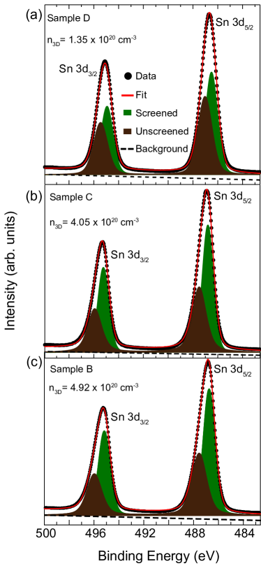
Figure 4 depicts the Sn 3d core level XPS spectra together with the Voigt function fits after subtraction of a Shirley background, for three representative samples of different total carrier density . The Sn 3d spectral lineshapes display an asymmetry to the high binding energy side of the peak, which increases with increasing carrier density. In metallic systems, the asymmetry in core photoemission spectra arises from intrinsic plasmon excitations associated with the creation of the core hole, which results in an additional component satellite to the main core line [63, 64]. It is known that the Coulomb potential of the core hole creates a localized trap state by capturing a conduction electron [65, 66, 67]. In La:BaSnO systems, the conduction band is derived from highly dispersive Sn 5s bands [43, 32], and the observed doping effect in the Sn 3d core level lineshape is most probably due to screening responses of the conduction electrons introduced by doping [63]. Therefore, two doublet components were used to fit the Sn 3d spectra assuming that the Koopmans’ state (i.e. the excited state after the removal of a core electron from the atom) is projected into screened and unscreened final eigenstates [63].
To understand the effect of increasing carrier density in the Sn 3d core level, the spectral lineshape of four samples (B, C, D and E) of different values were investigated and the analysis results are summarized in Table 4. The core lines were fitted to two Voigt components, which give an excellent description of the overall line shape of the spectra. In each spectrum, the main component is the peak at low binding energy labeled “screened”. This peak has a dominant Gaussian line shape. The component at high binding energy labeled “unscreened” is dominantly Lorentzian, which is a satellite associated with intrinsic plasmon excitations [67]. This peak is broader than the screened component, as evidenced by their FWHM values. Similar satellite structures were reported in the Sn 3d and In 3d core photoemission spectra of binary transparent conducting oxides (Sb-doped SnO [64, 68, 63], InO–ZnO [69] and Sn-doped InO [70, 67]).
To better visualize the connection between carrier density and the screened/unscreened intensity and energy, the evolution of both the satellite energy and the intensity of the peaks with is plotted [Fig. 5]. As can be seen from Table 4, the binding energy value of the main component suggests a valence state of for Sn [71, 72]; and the energy separation (satellite energy) between the main and satellite components increases with [Fig. 5(a)]. Furthermore, the relative intensity of the screened component increases with increasing , while that of the unscreened peak decreases. This is indicated in Fig. 5(b) by the increase of the intensity ratio of the peaks, conveying good agreement with previous reports [73, 65, 64, 69, 67]. The discrepancy at the lowest (sample E) could be ascribed to the fact that the thickness of this sample, 100 nm, surpasses a critical thickness above which additional structural defects are induced in the film [74, 75]. We speculate that defect scattering dominates, as only 15% of the carriers are activated compared to more than 50% activation for the other samples.
For fitting the spectra, the Gauss-Lorentz ratio was allowed to vary freely. Boundaries were set for the satellite energy. These constraints were applied to the lower limit of the position of the unscreened peak with the consideration that the satellite energy corresponds to the plasmon energy (i.e., the surface plasmon energy) and increases with the carrier density [64, 63, 67, 76, 77]. Since the surface plasmon energy is proportional to the carrier density [64, 70], the constraints were such that the satellite energy would be in the range of values reported for photoemission spectra of the 3d orbitals in binary transparent conducting oxides [64, 63, 69, 67] with comparable values as in samples B, C, D and E. Therefore, the consistent observation of a narrower low binding energy peak and a broader high binding energy peak supports the applicability of the plasmon model to the analysis of the Sn 3d core XPS spectra in these films, which is consistent with previously reported Sn 3d core level spectra in Sb-doped SnO samples [64, 68, 63].
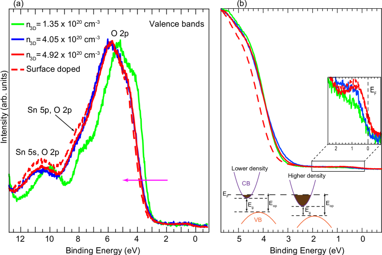
Next, the effect of increasing carrier density on the valence and conduction band spectra was explored. The same La:BaSnO samples characterized for the core level spectra were used. The XPS spectra of the valence and conduction bands are depicted in Figs. 6(a) and 6(b), respectively.
Three main features are observed in the valence band spectra: (i) a mixture of Sn 5s and bonding O 2p orbitals located at 10.6 eV; (ii) the states at 8.3 eV originating from hybridized Sn 5p and O 2p orbitals; and (iii) the bands at binding energies between 4 and 6 eV associated with O 2p bonding or anti-bonding character [78, 79, 80]. Additionally, shifts of the valence band leading edge to high binding energies upon increasing carrier density can be observed. This indicates an increase in the optical band gap as proposed previously in ellipsometry and HAXPES results [32, 25, 81]. These shifts are correlated to the shifts observed in the core levels [See section S2 of the supplementary information], as well as to the increasing asymmetry in the Sn 3d core lines. Similar trends were observed in other degenerate doped transparent conducting oxides, which were attributed to the increasing occupation of the states in the conduction band [63, 69, 67]. It is noteworthy that an opposite trend (i.e., shift of the valence band spectra toward lower binding energies with increases in La doping) was reported in recent angle resolved photoemission spectroscopy (ARPES) experiments on La:BaSnO3 films, and it was suggested to originate from the opposite evolution of surface and bulk chemical potentials [46].
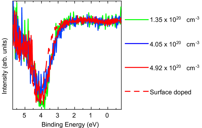
To explore further spectral features arising from occupation of the conduction bands, high resolution scans around the valence band leading edges were acquired [Fig. 6(b)]. To achieve an adequate signal to noise ratio and resolve the fine features in the region close to the Fermi energy (E), each spectrum was acquired over a period of about 20 hours. A peak at 4 eV deriving from O 2p orbitals is observed in all spectra as indicated by their first derivatives [see Fig. S5 of the supplementary information] [46, 45]. For the contaminated surface (sample with the highest intentionally exposed to contamination in the load lock), a shift to higher binding energy of 0.23 eV is clearly visible in the leading edge valence band spectrum [see red dashed curve in Fig. 6(b)]. Furthermore, a bump is detectable in all spectra in the region between 2 eV and E [see top right inset in Fig. 6(b)]. The spectra exhibit a weak structure close to E, which terminates in a sharp Fermi edge. This structure is associated with occupied states in the conduction band (Sn 5s orbital character with a small contribution from O 2p orbitals) [43, 32]. Moreover, the intensity of this CBM peak is observed to increase in the contaminated surface as evidenced by the red dashed curve [see top right inset in Fig. 6(b)]. This suggests that exposure of the surface to contamination results in increasing occupied states in the conduction band. We attribute this behavior to the Moss-Burstein effect, i.e., the apparent optical band gap of the material is increased as the absorption edge is pushed to higher energies as a result of some states close to the conduction band being populated [see, bottom left inset in Fig. 6(b)] [82, 83]. Indeed, the valence band shifts associated with the increasing density of electrons occupying the conduction band were reported in several transparent conducting oxides, resulting in the increase of the intensity of the conduction band feature [67, 32, 69, 84, 25].
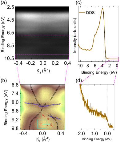
To date, few ARPES studies of the electronic band structure of La:BaSnO3 and BaSnO3 films have been reported [46, 45, 44]. In Fig. 7, we present the ARPES data of the band structure of a representative La:BaSnO3 film (Sample D) exposed to air for days before cleaning in vacuum [85]. These data were collected at room temperature. Although ARPES is a very surface sensitive technique and the samples were exposed to ambient conditions, valence band dispersion is observed from about 3.10 to 10.62 eV [Fig. 7(a)]. The fact that these bands are not clearly resolved is understood in terms of the need for a very particular surface treatment associated with ex-situ ARPES measurements [44]. Figure 7(b) depicts a high-resolution 2D ARPES map in the binding energies ranging from 6.8 to 9.8 eV around the hybridized Sn 5s and O 2p states. Some highly dispersive bands are resolved: the black markers overlaying the dispersing bands are extracted band dispersions obtained from peak fitting of the momentum distribution curves (MDCs), whereas the blue markers are for bands fitted to peaks in the energy distribution curves (EDCs). Figure 7(c) represents the density of states (DOS) integrated from the ARPES map (i.e., EDC obtained from the ARPES map over the entire momentum space). The DOS spectrum exhibits well resolved band features that are similar to the XPS valence band spectra [Fig. 6(a)]. The Fermi-Dirac edge straddling 0 eV is visible [Fig. 7(d)], and a linear extrapolation of the valence band leading edge reveals that the VBM is situated at eV [see, black dashed line in Fig. 7(c)]. The extracted VBM value is in close agreement to previous theoretical and experimental values [43, 46, 45, 44]. For this sample investigated in both XPS and ARPES, the same value for the VBM is obtained from both techniques; and the CBM is not well developed as evidenced by the data for both techniques shown in the insets in Fig. 6b and Fig. 7d.
In summary, we have systematically investigated the evolution of electronic states in the band structure of La:BaSnO films at different La doping levels. A close connection between the transport and the spectroscopic characteristics is demonstrated. In particular, increasing the carrier concentration in the conduction band by doping is observed to significantly affect the core and valence band spectra. The Sn 3d core line shape presents a pronounced asymmetry variation with the carrier density, and is fitted following the plasmon model applicable to metallic systems. Scans around the valence band spectra allowed the detection of the occupied states in the conduction bands. It is determined that surface contamination could potentially induce surface carrier accumulation, supported by the increase in the intensity of the CBM detected in the surface exposed to contamination. This study presents a detailed characterization of the chemical composition of the near-surface region of La:BaSnO, and it provides a better picture of the interplay between the doping concentration, electronic band structure and transport properties of epitaxial La:BaSnO films. The ARPES data presented in this study highlight the challenge of surface preparation for ex-situ ARPES measurements of epitaxial La:BaSnO films and heterostructures. Preferably, a portable vacuum suitcase is ideal for long-distance transport of epitaxial La:BaSnO films in UHV conditions to perform further in situ ARPES analysis at different locations [86] and/or development of protective capping methods for in situ capping to avoid any possible surface contamination when films are exposed to ambient conditions.
Supplementary Material
See supplementary material for details on electronic transport measurements, additional microstructural and photoemission spectroscopy characterizations of La:BaSnO3 films and heterostructures.
The authors grateful acknowledge fruitful discussions and technical support by Kathrin Küster. B. P. Doyle, A. P. Nono Tchiomo, A. R. E. Prinsloo and E. Carleschi acknowledge funding support from the National Research Foundation (NRF) of South Africa under Grant Nos. 93205, 90698, 99030, and 111985. W. Sigle and P. van Aken acknowledge funding from the European Union’s Horizon 2020 research and innovation programme under grant agreement No. 823717 -ESTEEM3.
REFERENCES
References
- Kim et al. [2012a] H. J. Kim, U. Kim, H. M. Kim, T. H. Kim, H. S. Mun, B.-G. Jeon, K. T. Hong, W.-J. Lee, C. Ju, K. H. Kim, and K. Char, Appl. Phys. Express 5, 061102 (2012a).
- Kim et al. [2012b] H. J. Kim, U. Kim, T. H. Kim, J. Kim, H. M. Kim, B.-G. Jeon, W.-J. Lee, H. S. Mun, K. T. Hong, J. Yu, K. Char, and K. H. Kim, Phys. Rev. B 86, 165205 (2012b).
- Luo et al. [2012] X. Luo, Y. S. Oh, A. Sirenko, P. Gao, T. A. Tyson, K. Char, and S.-W. Cheong, Appl. Phys. Lett. 100, 172112 (2012).
- Lee et al. [2017] W.-J. Lee, H. J. Kim, J. Kang, D. H. Jang, T. H. Kim, J. H. Lee, and K. H. Kim, Annu. Rev. Mater. Res. 47, 391 (2017), and references therein .
- Kim et al. [2015] U. Kim, C. Park, T. Ha, Y. M. Kim, N. Kim, C. Ju, J. Park, J. Yu, J. H. Kim, and K. Char, APL Mater. 3, 036101 (2015).
- Yue et al. [2018] J. Yue, A. Prakash, M. C. Robbins, S. J. Koester, and B. Jalan, ACS Appl. Mater. Interfaces 10, 21061 (2018).
- Wang et al. [2019] Z. Wang, H. Paik, Z. Chen, D. A. Muller, and D. G. Schlom, APL Mater. 7, 022520 (2019).
- Zhang et al. [2017] Y. Zhang, M. P. K. Sahoo, and J. Wang, Phys. Chem. Chem. Phys. 19, 7032 (2017).
- Shin et al. [2013] S. S. Shin, J. S. Kim, J. H. Suk, K. D. Lee, D. W. Kim, J. H. Park, I. S. Cho, K. S. Hong, and J. Y. Kim, ACS Nano 7, 1027 (2013).
- Park et al. [2016] J. Park, U. Kim, and K. Char, Appl. Phys. Lett. 108, 092106 (2016).
- Fortunato et al. [2016] E. Fortunato, D. Ginley, H. Hosono, and D. C. Paine, MRS Bulletin 32, 2007 (2016).
- Li et al. [2017] J. Li, Z. Ma, R. Sa, and K. Wu, RSC Adv. 7, 32703 (2017).
- Rajasekaran et al. [2020] P. Rajasekaran, M. Arivanandhan, Y. Kumaki, R. Jayavel, Y. Hayakawa, and M. Shimomura, CrystEngComm. 22, 5363 (2020).
- Wu and Gao [2018] T. Wu and P. Gao, Materials 11, 999 (2018).
- Cho et al. [2019a] H. J. Cho, B. Feng, T. Onozato, M. Wei, A. V. Sanchela, Y. Ikuhara, and H. Ohta, Phys. Rev. Materials 3, 094601 (2019a).
- Ismail-Beigi et al. [2015] S. Ismail-Beigi, F. J. Walker, S.-W. Cheong, K. M. Rabe, and C. H. Ahn, APL Materials 3, 062510 (2015).
- Krishnaswamy et al. [2016] K. Krishnaswamy, L. Bjaalie, B. Himmetoglu, A. Janotti, L. Gordon, and C. G. Van de Walle, Appl. Phys. Lett. 108, 083501 (2016).
- Ginley and Bright [2000] D. S. Ginley and C. Bright, MRS Bulletin 25, 15 (2000).
- Prakash et al. [2017a] A. Prakash, P. Xu, A. Faghaninia, S. Shukla, J. W. Ager, C. S. Lo, and B. Jalan, Nat. Commun. 8, 15167 (2017a).
- Alaan et al. [2019] U. S. Alaan, F. J. Wong, J. J. Ditto, A. W. Robertson, E. Lindgren, A. Prakash, G. Haugstad, P. Shafer, A. T. N’Diaye, D. Johnson, E. Arenholz, B. Jalan, N. D. Browning, and Y. Suzuki, Phys. Rev. Materials 3, 124402 (2019).
- Sanchela et al. [2018] A. V. Sanchela, M. Wei, H. Zensyo, B. Feng, J. Lee, G. Kim, H. Jeen, Y. Ikuhara, and H. Ohta, Appl. Phys. Lett. 112, 232102 (2018).
- Cho et al. [2019b] H. J. Cho, T. Onozato, M. Wei, A. Sanchela, and H. Ohta, APL Mater. 7, 022507 (2019b).
- Yu et al. [2016] S. Yu, D. Yoon, and J. Son, Appl. Phys. Lett. 108, 262101 (2016).
- Yoon et al. [2018] D. Yoon, S. Yu, and J. Son, NPG Asia Mater. 10, 363 (2018).
- Niedermeier et al. [2017] C. A. Niedermeier, S. Rhode, K. Ide, H. Hiramatsu, H. Hosono, T. Kamiya, and M. A. Moram, Phys. Rev. B 95, 161202 (2017).
- Wadekar et al. [2014] P. V. Wadekar, J. Alaria, M. O’Sullivan, N. L. O. Flack, T. D. Manning, L. J. Phillips, K. Durose, O. Lozano, S. Lucas, J. B. Claridge, and M. J. Rosseinsky, Appl. Phys. Lett. 105, 052104 (2014).
- Nono Tchiomo et al. [2019] A. P. Nono Tchiomo, W. Braun, B. P. Doyle, W. Sigle, P. van Aken, J. Mannhart, and P. Ngabonziza, APL Mater. 7, 041119 (2019).
- Fan et al. [2018] F.-Y. Fan, W.-Y. Zhao, T.-W. Chen, J.-M. Yan, J.-P. Ma, L. Guo, G.-Y. Gao, F.-F. Wang, and R.-K. Zheng, Appl. Phys. Lett. 113, 202102 (2018).
- Mizoguchi et al. [2013] H. Mizoguchi, P. Chen, P. Boolchand, V. Ksenofontov, C. Felser, P. W. Barnes, and P. M. Woodward, Chem. Mater. 25, 3858 (2013).
- Fujiwara et al. [2017] K. Fujiwara, K. Nishihara, J. Shiogai, and A. Tsukazaki, Appl. Phys. Lett. 110, 203503 (2017).
- Raghavan et al. [2016] S. Raghavan, T. Schumann, H. Kim, J. Y. Zhang, T. A. Cain, and S. Stemmer, APL Mater. 4, 016106 (2016).
- Lebens-Higgins et al. [2016] Z. Lebens-Higgins, D. O. Scanlon, H. Paik, S. Sallis, Y. Nie, M. Uchida, N. F. Quackenbush, M. J. Wahila, G. E. Sterbinsky, D. A. Arena, J. C. Woicik, D. G. Schlom, and L. F. J. Piper, Phys. Rev. Lett. 116, 027602 (2016).
- Paik et al. [2017] H. Paik, Z. Chen, E. Lochocki, A. Seidner H., A. Verma, N. Tanen, J. Park, M. Uchida, S. Shang, B.-C. Zhou, M. Brützam, R. Uecker, Z.-K. Liu, D. Jena, K. M. Shen, D. A. Muller, and D. G. Schlom, APL Mater. 5, 116107 (2017).
- Wang et al. [2020] H. Wang, A. Prakash, K. Reich, K. Ganguly, B. Jalan, and C. Leighton, APL Mater. 8, 071113 (2020).
- Postiglione et al. [2021] W. M. Postiglione, K. Ganguly, H. Yun, J. S. Jeong, A. Jacobson, L. Borgeson, B. Jalan, K. A. Mkhoyan, and C. Leighton, Phys. Rev. Materials 5, 044604 (2021).
- Zhang et al. [2021] R. Zhang, X. Li, J. Bi, S. Zhang, S. Peng, Y. Song, Q. Zhang, L. Gu, J. Duan, and Y. Cao, APL Mater. 9, 061103 (2021).
- Ganguly et al. [2017] K. Ganguly, A. Prakash, B. Jalan, and C. Leighton, APL Mater. 5, 056102 (2017).
- Ganguly et al. [2015] K. Ganguly, P. Ambwani, P. Xu, J. S. Jeong, K. A. Mkhoyan, C. Leighton, and B. Jalan, APL Mater. 3, 062509 (2015).
- He et al. [2021] Y. He, R. Wei, C. Zhou, W. Cheng, X. Ding, C. Shao, L. Hu, W. Song, X. Zhu, and Y. Sun, Cryst. Growth Des. 21, 5800 (2021).
- Prakash et al. [2017b] A. Prakash, P. Xu, X. Wu, G. Haugstad, X. Wang, and B. Jalan, J. Mater. Chem. C 5, 5730 (2017b).
- Lee et al. [2016] W.-J. Lee, H. J. Kim, E. Sohn, T. H. Kim, J.-Y. Park, W. Park, H. Jeong, T. Lee, J. H. Kim, K.-Y. Choi, and K. H. Kim, Appl. Phys. Lett. 108, 082105 (2016).
- Scanlon [2013] D. O. Scanlon, Phys. Rev. B 87, 161201 (2013).
- Sallis et al. [2013] S. Sallis, D. O. Scanlon, S. C. Chae, N. F. Quackenbush, D. A. Fischer, J. C. Woicik, J.-H. Guo, S. W. Cheong, and L. F. J. Piper, Appl. Phys. Lett. 103, 042105 (2013).
- Soltani et al. [2020] S. Soltani, S. Hong, B. Kim, D. Kim, J. K. Jung, B. Sohn, T. W. Noh, K. Char, and C. Kim, Phys. Rev. Materials 4, 055003 (2020).
- Joo et al. [2017] B. S. Joo, Y. J. Chang, L. Moreschini, A. Bostwick, E. Rotenberg, and M. Han, Curr. Appl. Phys. 17, 595 (2017).
- Lochocki et al. [2018] E. B. Lochocki, H. Paik, M. Uchida, D. G. Schlom, and K. M. Shen, Appl. Phys. Lett. 112, 181603 (2018).
- Braun et al. [2020] W. Braun, M. Jäger, G. Laskin, P. Ngabonziza, W. Voesch, P. Wittlich, and J. Mannhart, APL Mater. 8, 071112 (2020).
- Ngabonziza et al. [2016] P. Ngabonziza, M. P. Stehno, H. Myoren, V. A. Neumann, G. Koster, and A. Brinkman, Adv. Electron. Mater. 2, 1600157 (2016).
- Ngabonziza et al. [2018a] P. Ngabonziza, Y. Wang, and A. Brinkman, Phys. Rev. Materials 2, 044204 (2018a).
- Ngabonziza [2022] P. Ngabonziza, Nanotechnology 33, 192001 (2022).
- Nono Tchiomo et al. [2018] A. P. Nono Tchiomo, G. Babu-Geetha, E. Carleschi, P. Ngabonziza, and B. P. Doyle, Surf. Sci. Spectra 25, 024001 (2018).
- Hove and Tong [1979] M. A. V. Hove and S. Y. Tong, Surface crystallography by LEED: theory, computation and structural results, (Springer, Berlin, 1979).
- Liu et al. [2021] Y. Liu, H. Huang, L. Xue, J. Sun, X. Wang, P. Xiong, and J. Zhu, Nanoscale 13, 19840 (2021).
- Wang et al. [2015] W. Y. Wang, Y. L. Tang, Y. L. Zhu, J. Suriyaprakash, Y. B. Xu, Y. Liu, B. Gao, S.-W. Cheong, and X. L. Ma, Sci. Rep. 5, 16097 (2015).
- Yun et al. [2018] H. Yun, M. Topsakal, A. Prakash, K. Ganguly, C. Leighton, B. Jalan, R. M. Wentzcovitch, K. A. Mkhoyan, and J. S. Jeong, J. Vac. Sci. Technol. 36, 031503 (2018).
- Larramona et al. [1989] G. Larramona, C. Gutiérrez, I. Pereira, M. R. Nunes, and F. M. A. da Costa, J. Chem. Soc. Faraday Trans. 1 85, 907 (1989).
- Jaim et al. [2017] H. M. I. Jaim, S. Lee, X. Zhang, and I. Takeuchi, Appl. Phys. Lett. 111, 172102 (2017).
- Rault et al. [2013] J. E. Rault, G. Agnus, T. Maroutian, V. Pillard, P. Lecoeur, G. Niu, B. Vilquin, M. G. Silly, A. Bendounan, F. Sirotti, and N. Barrett, Phys. Rev. B 87, 155146 (2013).
- Li et al. [2005] X. L. Li, B. Chen, H. Y. Jing, H. B. Lu, B. R. Zhao, Z. H. Mai, and Q. J. Jia, Appl. Phys. Lett. 87, 222905 (2005).
- Li et al. [2008] X. L. Li, H. B. Lu, M. Li, Z. Mai, H. Kim, and Q. J. Jia, Appl. Phys. Lett. 92, 012902 (2008).
- Colón Santana [2015] J. A. Colón Santana, Quantitative Core Level Photoelectron Spectroscopy (Morgan & Claypool Publishers, San Rafael, USA, 2015).
- Armen et al. [1985] G. B. Armen, T. Åberg, K. R. Karim, J. C. Levin, B. Crasemann, G. S. Brown, M. H. Chen, and G. E. Ice, Phys. Rev. Lett. 54, 182 (1985).
- Egdell et al. [1999] R. G. Egdell, J. Rebane, T. J. Walker, and D. S. L. Law, Phys. Rev. B 59, 179 (1999).
- Egdell et al. [2003] R. Egdell, T. Walker, and G. Beamson, J. Electron Spectrosc. Relat. Phenom. 128, 59 (2003).
- Chazalviel et al. [1977] J. N. Chazalviel, M. Campagna, G. K. Wertheim, and H. R. Shanks, Phys. Rev. B 16, 697 (1977).
- Campagna et al. [1975] M. Campagna, G. K. Wertheim, H. R. Shanks, F. Zumsteg, and E. Banks, Phys. Rev. Lett. 34, 738 (1975).
- Körber et al. [2010] C. Körber, V. Krishnakumar, A. Klein, G. Panaccione, P. Torelli, A. Walsh, J. L. F. Da Silva, S.-H. Wei, R. G. Egdell, and D. J. Payne, Phys. Rev. B 81, 165207 (2010).
- Cox et al. [1982] P. Cox, R. Egdell, C. Harding, A. Orchard, W. Patterson, and P. Tavener, Solid State Commun. 44, 837 (1982).
- Jia et al. [2013] J. Jia, N. Oka, and Y. Shigesato, J. Appl. Phys. 113, 163702 (2013).
- Christou et al. [2000] V. Christou, M. Etchells, O. Renault, P. J. Dobson, O. V. Salata, G. Beamson, and R. G. Egdell, J. Appl. Phys. 88, 5180 (2000).
- Morgan and Van Wazer [1973] W. E. Morgan and J. R. Van Wazer, J. Phys. Chem. 77, 964 (1973).
- Crist [2000] V. B. Crist, Handbook of monochromatic XPS spectra: The elements of native oxides (John Wiley & Sons, Chichester, 2000).
- Langreth [1973] D. C. Langreth, Theory of plasmon effects in high-energy spectroscopy, in Proceedings of Nobel Symposium 24 in Medicine and Natural Science, edited by B. Lundqvist and S. Lundqvist (Academic Press, New York and London, 1973) pp. 210–222.
- Berger et al. [1988] P. R. Berger, K. Chang, P. Bhattacharya, J. Singh, and K. Bajaj, Appl. Phys. Lett. 53, 684 (1988).
- Kneiß et al. [2020] M. Kneiß, P. Storm, A. Hassa, D. Splith, H. von Wenckstern, M. Lorenz, and M. Grundmann, APL Mater. 8, 051112 (2020).
- Payne et al. [2005] D. J. Payne, R. G. Egdell, W. Hao, J. S. Foord, A. Walsh, and G. W. Watson, Chem. Phys. Lett. 411, 181 (2005).
- Glans et al. [2005] P.-A. Glans, T. Learmonth, K. E. Smith, J. Guo, A. Walsh, G. W. Watson, F. Terzi, and R. G. Egdell, Phys. Rev. B 71, 235109 (2005).
- Themlin et al. [1990] J. M. Themlin, R. Sporken, J. Darville, R. Caudano, J. M. Gilles, and R. L. Johnson, Phys. Rev. B 42, 11914 (1990).
- Vasheghani Farahani et al. [2014] S. K. Vasheghani Farahani, T. D. Veal, J. J. Mudd, D. O. Scanlon, G. W. Watson, O. Bierwagen, M. E. White, J. S. Speck, and C. F. McConville, Phys. Rev. B 90, 155413 (2014).
- Kövér et al. [1995] L. Kövér, G. Moretti, Z. Kovács, R. Sanjinés, I. Cserny, G. Margaritondo, J. Pálinkás, and H. Adachi, J. Vac. Sci. Technol. A 13, 1382 (1995).
- Seo et al. [2014] D. Seo, K. Yu, Y. Jun Chang, E. Sohn, K. Hoon Kim, and E. J. Choi, Appl. Phys. Lett. 104, 022102 (2014).
- Burstein [1954] E. Burstein, Phys. Rev. 93, 632 (1954).
- Moss [1954] T. S. Moss, Proc. Phys. Soc. B 67, 775 (1954).
- Mudd et al. [2014] J. J. Mudd, T.-L. Lee, V. Muñoz Sanjosé, J. Zúñiga Pérez, D. J. Payne, R. G. Egdell, and C. F. McConville, Phys. Rev. B 89, 165305 (2014).
- [85] The La:BaSnO3 films were prepared at the Max Planck Institute for Solid State Research, Stuttgart, Germany and transported at ambient conditions for further spectroscopic measurements (XPS and ARPES) to the University of Johannesburg, South Africa. Details on the cleaning procedure of the samples and spectroscopic measurements are presented in supplemantry information .
- Ngabonziza et al. [2018b] P. Ngabonziza, M. P. Stehno, G. Koster, and A. Brinkman, In Situ Characterization Tools for Bi2Te3 Topological Insulator Nanomaterials, in In-situ Characterization Techniques for Nanomaterials, edited by C. S. Kumar (Springer Berlin Heidelberg, 2018) pp. 223–250.
*Supplementary Information:
Combined Spectroscopy and Electrical Characterization of La:BaSnO
Thin Films and Heterostructures
Arnaud P. Nono Tchiomo,1, 2 Emanuela Carleschi,1 Aletta R. E. Prinsloo,1 Wilfried Sigle,3 Peter A. van Aken,3 Jochen Mannhart,3 Prosper Ngabonziza, Bryan P. Doyle,
1Department of Physics, University of Johannesburg, P.O. Box 524, Auckland Park 2006, Johannesburg, South Africa
2Van der Waals-Zeeman Institute, Institute of Physics, Science Park 904, 1098 XH Amsterdam, The Netherlands
3Max Planck Institute for Solid State Research, Heisenbergstr. 1, 70569 Stuttgart, Germany
S1: Electronic Transport Measurements and Microstructural Characterizations
All La:BaSnO3 samples were grown by pulsed laser deposition at an optimal target-substrate distance of 56 mm. The deposition parameters are given in Table 1. After growth of La:BaSnO3 films, Au/Ti contacts (45 nm thick) that provide electrical connections to the sample were added to the samples’ corners using standard photolithography methods [Fig. S1(a)]. Basic electrical characterizations of the samples were performed using a physical property measurement system (PPMS) in four-point configuration with an excitation current of 1A.
| Sample | Thin film | Substrate | Deposition | O partial | Laser | Laser repetition |
|---|---|---|---|---|---|---|
| layer | temperature | pressure | fluence | rate | ||
| (C) | (mbar) | (J cm) | (Hz) | |||
| BaSnO (100 nm) | 850 | 1.5 | 4 | |||
| A | 6% La:BaSnO (25 nm) | DyScO | 850 | 1.5 | 1 | |
| B | BaSnO (100 nm) | TbScO | 850 | 1.5 | 5 | |
| 6% La:BaSnO (25 nm) | 850 | 1.5 | 5 | |||
| C | 6% La:BaSnO (25 nm) | SrTiO | 850 | 1.5 | 1 | |
| D | 2% La:BaSnO (25 nm) | TbScO | 850 | 1.5 | 1 | |
| BaSnO (25 nm) | 850 | 1.5 | 1 | |||
| E | 4% La:BaSnO (100 nm) | SrTiO | 850 | 1.5 | 1 |
The scanning transmission electron microscopy (STEM) and electron energy loss spectroscopy (EELS) investigations were performed using a Cs-probe-corrected JEOL JEM-ARM200F. The EELS measurements were performed on the cross-section of BaSnO buffered samples, and the electron beam was focused on the buffer layer and the La:BaSnO film layer regions. Spectra from areas without and with La could then be compared, to see whether the doping alters or changes the oxidation state of the Sn.
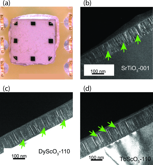
In epitaxial thin film growth, a buffer layer can be employed to boost both the structural and electronic properties of the film [1, 2, 3] . The primary role of this additional layer is to reduce the density of defects, and in particular, the concentration of threading dislocations, which result in carrier density and carrier mobility reduction [1, 2, 3]. These dislocations are known to originate from misfit dislocations, which are generated at the film/substrate interface due to the large lattice mismatch between the as-deposited film layer and the substrate [4, 5, 6]. Figures S1(b)-(d) depict scanning transmission electron microscopy (STEM) micrographs of BaSnO3/SrTiO3, BaSnO3/DyScO3 and BaSnO3/TbScO3 heterostructures. Dense edge-type threading dislocations identified as vertical lines running across the film from the interface can be observed [4, 6]. A quantitative analysis of these threading dislocations carried out by counting the number of lines in 500 nm by 16 nm thick specimens gives a dislocation density of cm in the film prepared on SrTiO3, and cm in the films grown with DyScO3 and TbScO3 substrates. This high concentration of threading dislocations acts as charge traps, and was reported to be responsible for the low activation rate of the carrier, as well as for the limitation of the electron mobility in La:doped BaSnO3 systems [1, 7, 8].
S2: Photoemission Spectroscopy Measurements
The La:BaSnO3 thin films and heterostructures were grown using pulsed laser deposition at the Max Planck Institute for Solid State Research, Stuttgart Germany. After electronic transport characterizations, samples were transported in ambient conditions to the University of Johannesburg in South Africa for further spectroscopic measurements. X-ray photoemission spectroscopy (XPS) and angle resolved photoemission spectroscopy (ARPES) spectra were collected using a SPECS PHOIBOS 150 hemispherical electron energy analyzer. The base pressure in the analysis chamber during acquisition of the core and valence XPS data was 3 mbar. These were measured using monochromatized Al Kα and Ag Lα excitation sources, emitting photons of energies of 1486.71 eV and 2984.31 eV, respectively. The experimental resolutions with these two sources were 580 and 960 meV, respectively. To investigate the electronic band structure, we also excited the valence electrons of the samples using a He I source delivering photons of 21.2 eV. For these ARPES measurements, the experimental resolution was 120 meV.
As the samples had been exposed to air under ambient conditions, their surfaces were thoroughly cleaned in vacuum prior to spectroscopic measurements. The cleaning procedure consisted of annealing in O environment at the temperature of C in a preparation chamber maintained at 7 mbar. The annealing procedure consisted of several cycles of 2 hours each and it was done using an e-beam heater at a maximum electron emission power of 3.5 W. The temperature was indicated by a pyrometer set to an emissivity of 0.1. The cleanliness of the samples was monitored by recording the low-energy electron diffraction (LEED) patterns (to inspect the surface structure) directly after an annealing cycle [Fig. S2(a)], as well as by tracking the C 1s signal in the XPS survey scans [Fig. S2(c)] and by tracking the O 1s, Sn 3d and Ba 3d levels before and after surface cleaning [see, Fig. S3, Fig. S5]. LEED was also used for the determination of the orientation of the surfaces before ARPES measurements. Figure S2(a) and Fig. S2(b) depict representative LEED images of the La:BaSnO3 surface at different stages in the high-temperature cleaning process, and at different electron energies (clean surface), respectively.
References
[1] A. P. Nono Tchiomo, W. Braun, B. P. Doyle, W. Sigle, P. van Aken,
J. Mannhart, and P. Ngabonziza, APL Mater. 7, 041119 (2019).
[2] S. Nakamura, Jpn. J. Appl. Phys. 30, L1705 (1991).
[3] Y. Huang, X. D. Chen, S. Fung, C. D. Beling, C. C. Ling, Z. F. Wei, S. J. Xu, and C.
Y. Zhi,
J. Appl. Phys. 96, 1120 (2004).
[4] H. Paik, Z. Chen, E. Lochocki, H. Ariel Seidner, A. Verma, N. Tanen, J. Park, M. Uchida,
S. Shang, B. C. Zhou, M. Brützam, R. Uecker, Z. K. Liu, D. Jena, K. M. Shen, D. A. Muller, and
D. G. Schlom, APL Mater. 5, 116107 (2017).
[5] S. Raghavan, T. Schumann, H. Kim, J. Y. Zhang, T. A. Cain, and S. Stemmer,
APL Mater. 4, 016106 (2016).
[6] J. Shiogai, K. Nishihara, K. Sato, and A. Tsukazaki, AIP Adv. 6, 065305 (2016).
[7] Z. Lebens-Higgins, D. O. Scanlon, H. Paik, S. Sallis, Y. Nie, M. Uchida, N. F. Quackenbush,
M. J. Wahila, G. E. Sterbinsky, D. A. Arena, J. C. Woicik, D. G. Schlom, and L. F. Piper,
Phys. Rev. Lett. 116, 027602 (2016).
[8] H. J. Kim, U. Kim, T. H. Kim, J. Kim, H. M. Kim, B. G. Jeon, W. J. Lee, H. S. Mun,
K. T. Hong, J. Yu, K. Char, and K. H. Kim, Phys. Rev. B 86, 165205 (2012).
[9] M. Sirena, N. Haberkorn, M. Granada, L. B. Steren, and J. Guimpel,
J. Appl. Phys. 105, 033902 (2009).
[10] J. Rubio-Zuazo, L. Onandia, P. Ferrer, and G. R. Castro,
Appl. Phys. Lett. 104, 021604 (2014).
[11] K. Wang, Y. Ma, and K. Betzler, Phys. Rev. B 76, 144431 (2007).
[12] A. Fujishima, X. Zhang, and D. A. Tryk, Surf. Sci. Rep. 63, 515 (2008).
[13] J. C. Yu, J. Yu, H. Y. Tanga, and L. Zhang, J. Mater. Chem. 12, 81 (2002).
[14] J. Zhuang, S. Weng, W. Dai, P. Liu, and Q. Liu, J. Phys. Chem. C 116, 25354 (2012).
[15] G. Greczynski, and L. Hultman, Prog. Mater. Sci. 107, 100591 (2020).
[16] E. Korin, N. Froumin, and S. Cohen, ACS Biomater. Sci. Eng. 3, 882 (2017).
[17] D. Cabrera-German, G. Gomez-Sosa, and A. Herrera-Gomez,
Surf. Interface Anal. 48, 252 (2016).