Superconducting density of states and bandstructure at the surface of the candidate topological superconductor Au2Pb
Abstract
The electronic bandstructure of Au2Pb has a Dirac cone which gaps when undergoing a structural transition into a low temperature superconducting phase. This suggests that the superconducting phase ( K) might hold topological properties at the surface. Here we make Scanning Tunneling Microscopy experiments on the surface of superconducting Au2Pb. We measure the superconducting gap and find a sizeable superconducting density of states at the Fermi level. We discuss possible origins for this finding in terms of superconductivity induced into surface states.
I Introduction
Recent efforts in band structure calculations have shown that it might be possible to obtain many intermetallic compounds with topologically non-trivial surface states [1, 2, 3]. Among these systems, a few become superconducting at low temperatures. It has been shown that superconductivity induced by proximity into a topologically non-trival electronic surface state can lead to triplet correlations and the appearance of Majorana modes at the surface [4, 5, 6, 7].
Here we analyze the compound Au2Pb. Au2Pb is a binary intermetallic system which crystallizes at room temperature in a cubic Laves phase [8, 9]. At low temperatures, Au2Pb presents an orthorhombic phase which is superconducting with K [10]. Band structure calculations of the room temperature cubic phase predict a bulk 3D Dirac cone due to symmetry allowed band crossings [8, 9]. The presence of the bulk Dirac cone is confirmed by angle resolved photoemission studies (ARPES) [11]. The lowered crystal symmetry of the low temperature phase lifts the band degeneracy and a gap opens at the bulk Dirac cone [8, 11]. As we show in detail below and represent schematically in Fig. 1(a), the parity of the bands is inverted at the gap, with the valence band having Au d-electron character and the conduction band Pb-sp3 character.
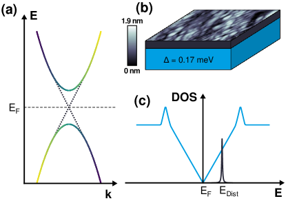
Experiments aiming to characterize surface states in the normal phase using optical conductivity have concluded that the contribution of the Dirac cone to the optical properties is masked by bulk bands crossing the Fermi energy [8, 11, 12]. In the superconducting phase, low temperature specific heat and thermal conductivity measurements have suggested that the bulk superconducting state of Au2Pb is fully gapped, agreeing with s-wave superconductivity [8, 13]. Here we analyze the superconducting properties using Scanning Tunnelling Microscope (STM) experiments on the surface of Au2Pb. We measure the superconducting density of states as a function of temperature and magnetic field. We find a superconducting gap value corresponding to a K within BCS theory and rough surfaces (Fig. 1(b)). The zero bias tunneling conductance is larger than about a third of the normal state density of states. We analyze the possible origin for the finite zero bias tunneling conductance in terms of the influence of defects on surface superconducting states, creating in-gap states schematically represented Fig. 1(c).
II Experiments and methods
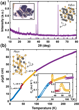
We synthesized the sample with a Pb flux growth method [14, 15, 8, 11]. Lumps of gold (99.99% Sempsa) and lead (99.999% Goodfellow) with a molar ratio Au:Pb 42:58 were put inside frit disk alumina crucibles [16] and sealed in an evacuated silica ampoule. The ampoule was then heated in 12 hours to 1150∘C, fast-cooled to 375∘C in 12 hours, held at this temperature for 6 hours and then slow-cooled to 275∘C in 22 hours. At this point the excess flux was decanted using a centrifuge. The obtained crystals typically had sizes of a few millimeters and showed clean triangular dark-silvered facets. We show powder x-ray data in Fig. 2(a) and a picture of the samples in the upper left inset. In Fig. 2(b) we show the resistivity as a function of temperature, and highlight with colors the different crystalline structures[9, 8]. In the lower right inset of Fig. 2(b) we show the specific heat vs temperature. These data mostly coincide with previous results in high quality single crystals of Au2Pb[8, 11]. Furthermore, in the insets of Fig. 2(a,b) we show the room and low temperature crystalline structures found in Au2Pb. At room temperature (violet points in Fig. 2(b)), the crystal structure is the cubic Laves phase (no. 227) [9]. It is based on the pyrochlore lattice, with Au atoms having a tetrahedric arrangement distributed inside a face centered cubic lattice of Pb atoms. The crystalline structures of the phase at intermediate temperatures (yellow and red points in Fig. 2(b)) are unknown. The structure of the low temperature phase (blue points in Fig. 2(b)) is derived from the cubic room temperature phase by small atomic distortions, giving orthorhombic , No. 60 [8].
We performed STM measurements using a home-made microscope described in Ref. 17 and the software described in Ref. [18]. The energy resolution of the tunneling conductance measurement setup is of 10 eV as shown measurements in Al with a similar set-up ( K) [19]. For image treatment, we use Refs. [18, 20]. We cut single crystalline samples in rectangular bars that are a few mm long and a fraction of a mm wide and mount them on the STM sample holder. The position of the sample holder can be modified to approach the long axis of the bar shaped sample to a blade in-situ at 4 K in such a way that the blade cleaves the sample and exposes a fresh surface. We exposed a surface perpendicular to a main crystalline axis of the cubic room temperature crystalline structure. Given the different structural transitions undergone upon cooling we can expect that we maintain a crystalline face at low temperatures. We observed large and flat areas over fields of view of a few hundreds of nm. We did not observe atomic resolution, but instead surfaces with elongated structures and a surface corrugation of order of the unit cell size (between 1 nm and 2 nm, see Fig. 4(a) and the Appendix).
First-principles calculations with spin-orbit coupling (SOC) were performed using the Quantum ESPRESSO package [21]. In our calculations we employed the generalized gradient approximation (GGA) with the Perdew-Burke-Ernzerhof (PBE) [22] exchange-correlation functional. We used fully-relativistic norm-conserving Pseudo DoJo pseudopotentials [23] and the electronic wave functions were expanded with well-converged kinetic energy cutoffs of 45 Ry and 180 Ry for the wavefunctions and charge density, respectively. The Brillouin zone was sampled with a Monkhorst-Pack [24] () -point mesh. Dispersion interactions to account for van der Waals interactions between the layers were considered by applying semi-empirical Grimme DFT-D3 corrections [25]. Structures were fully optimized using the Broyden-Fletcher-Goldfarb-Shanno (BFGS) algorithm [26] until the forces on each atom were smaller than Ry/au and the energy difference between two consecutive relaxation steps less than Ry. To analyze the surface bandstructure, we constructed a tight-binding model based on maximally localized Wannier functions [27, 28, 29] with Au and Pb orbitals in the range eV. We verified that we find the same results as in the first principles calculations within this energy range. To find the structure of surface states, we built surface spectral functions for a semi-infinite Au2Pb(001) surface via the surface Green’s function method [30, 31, 32, 33] as implemented in the WannierTools package [34].
III Results


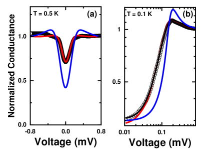
In Fig. 3 we show Scanning Tunneling Spectroscopy measurements of the superconducting gap of Au2Pb as a function of temperature. We see that there is no fully opened superconducting gap, but instead a large zero bias conductance. The quasiparticle peaks are also supressed with respect to the expected high peaks for a usual s-wave BCS superconductor. We deconvolute the local density of states () at each temperature, using the relation (see Refs. [35, 36, 37, 18] and the Appendix) and show the result in Fig. 3(b). From the density of states, we obtain the superconducting gap and its temperature dependence by following the quasiparticle peak positions in . We find a superconducting gap of meV. The BCS expression K provides KmeV using K, in close agreement with the value we find. Fig. 3(c) shows the temperature dependence of the superconducting gap up to K. roughly follows the temperature dependence of a fully opened s-wave superconducting gap expected within BCS theory.
The variations of the zero bias conductance as a function of the position are shown in Fig. 4(b). We observe variations that occur randomly over the whole surface. These are small, below about 10% of the normal state tunneling conductance. The magnetic field dependence is shown in the Appendix and is compatible with superconductivity having a low Ginzburg-Landau parameter and a coherence length of about 60 nm, as shown previously[8, 11]. Thus, we find a gap value which is compatible with specific heat measurements [8, 38, 11], but there is a sizeable finite density of states at the Fermi level which slightly varies as a function of the position.
We show the calculated electronic band structure of the low temperature orthorhombic phase in Fig. 5 (a). The overall shape coincides with previous calculations [8]. The Dirac cone of the room temperature cubic structure is opened by a gap along the line. The Fermi surface presents three bands crossings, the 15th, the 17th and the 19th bands. All are spin degenerate and produce three dimensional pockets with an intricate structure (Fig. 5(b)). The top and bottom of the bands crossing the Fermi level are just a few hundreds of meV from the Fermi level (Fig. 5(a)), confirming that Au2Pb is a low density semimetallic system. The 15th band (Fig. 5(c)) consists essentially of two hole pockets located at the top side and the edges of the Brillouin zone. It has a mixed Pb-p and Au-s,d character. The 17th band (Fig. 5(d)) consists of three electron pockets. One closed spherical pocket located well inside the Brillouin zone. Another one goes from the top to the bottom of the Brillouin zone, and the third one is located at the sides of the Brillouin zone. The 19th band (Fig. 5(e)) produces two electron pockets that are nested inside the 17th band pockets located at the sides of the Brillouin zone. Actually, these two pockets are nearly degenerate, as shown by the bandstructure between the and high symmetry points and both have a predominant Au-s,d character.

IV Discussion
Our tunneling conductance measurements (Fig. 3) show a single quasiparticle peak, showing that the gap magnitude is similar over the whole Fermi surface. However, we do not observe the zero density of states expected at a Fermi level for a usual isotropic s-wave superconductor. Furthermore, the measured at low temperatures (Fig. 3(b)) has a continous V-shaped variation for low energies, instead of a U or squarish shaped curve expected for a usual s-wave superconductor. These two findings differ from previous bulk specific heat measurements, which suggest instead a fully opened superconducting gap [8, 13].
One possible origin for modified superconducting properties at the surface is chemical degradation. This can be excluded in our case, because samples were cleaved at low temperatures in fully inert cryogenic vacuum. Thus, the STM measurements show that superconductivity at or close to the surface in Au2Pb is different than in the bulk.
To discuss this issue, we should first note that the surface roughness we find here is of order of the size of a unit cell (c-axis lattice parameter is of 1.1 nm). Previous ARPES experiments have found electronic surface states in polished surfaces of the room temperature cubic phase, whose roughness is above a unit cell size. Thus, the actual surface roughness does not disturb significantly the formation of surface states [11].
As a first scenario to discuss our results, we consider group theory applied to the low temperature orthorhombic phase. The Dirac cone of the high temperature tetragonal phase along the line opens in the low temperature orthorhomic phase, due to symmetry breaking allowed band mixing. The influence of this situation in superconductivity was recently analyzed in detail for the case of Au2Pb in Ref. [39]. For the orthorhombic point group (low temperature crystalline phase), only the superconducting states belonging to the trivial and the triplet representations have no nodes in the bulk and are thus compatible with the available bulk specific heat. Out of these, the state presents a linear Dirac band dispersion inside the bulk superconducting gap at the surface. This surface state is topologically protected by a zero-dimensional topological number that can be defined using the mirror symmetry [40, 41, 39]. The linear Dirac band dispersion inside the superconducting gap generates a linearly dependent superconducting density of states, with massless particles and thus zero states at the Fermi level. Atomic scale impurities within such a two-dimensional Dirac spectrum are known to produce distinct impurity resonances at an energy varying with the strength in the impurity and located within the linear portion of the spectrum (see Fig. 1(c)) [42]. These resonances have been observed inside the Dirac in-gap dispersion of cuprate superconductors and graphene and are inherent to a Dirac dispersion relation [43, 44, 42]. Thus, one possible origin for a finite zero bias tunneling conductance is that the surface corrugation generates in-gap states at different energies that overlap and provide a finite zero bias tunneling conductance with slight variations as a function of the position. This scenario would imply, however, a triplet bulk superconducting order parameter belonging to the representation. In absence of bulk spin-dependent measurements, such as Knight shift, there is no firm ground to assume triplet superconductivity in Au2Pb.
As a second scenario, we analyze in more detail the surface band structure in the normal state. We have calculated the surface Green’s function using DFT on a semi-infinite Au2Pb sample. We find well defined surface states located in the gaps of the bulk bandstructure for all surface terminations. Furthermore, the spin degeneracy of these surface states is lifted by spin orbit coupling. We show results on the (010) surface in Fig. 6(a,b). The topological invariant is one on this plane. We can clearly see that the gap along is closed at the surface by a Dirac cone. In addition, there are three surface states inside the gap, two of which cross the Fermi level at the center of the Dirac cone. These two surface states cross again the Fermi level close to . As we can see in Fig. 6(b), there are a number of additional surface states crossing the Fermi level along different directions of the Brillouin zone. Ginzburg showed that it was in principle possible to find superconductivity on a surface two-dimensional electron gas [45]. It has been shown that surface states of Ag and Au deposited on top of a superconductor show a superconducting density of states with a non-zero value at the Fermi level [46, 47]. Our measurements provide a similar result, suggesting that the opening of the superconducting gap at the surface states is incomplete.
We observe in our images that the surface corrugation is well above atomic size. The surface consists of irregular changes in height. However, absence of atomically flat surfaces does not modify surface states, as mentioned above and shown in Ref. [11]. Still, it induces disorder, which in turn smears out any sharp features in the density of states. The density of states we find in our experiments has a strong V-shape that can also be compatible with gapless s-wave superconductivity at surface states, the triplet order parameter discussed above as well as other possibilities that are not compatible with bulk measurements, such as nodal d-wave superconductivity with impurities[42]. In any case, the density of states we observe is strongly influenced by the disordered surface topography.
V Conclusion
In conclusion, we have determined the superconducting gap and density of states of Au2Pb. We find a superconducting gap magnitude of meV, compatible with K and BCS relation between the critical temperature and the gap. The superconducting density of states measured at the surface has a V-shape and a large finite value at zero bias, suggesting that there is a finite zero energy density of states. As possible origins for the finite density of states we discuss bulk triplet superconductivity and the concomitant Dirac states at the surface. We also discuss an intricate structure of surface states with incomplete superconducting gap opening.
Acknowledgements
This work was supported by the Spanish Research State Agency (PID2020-114071RB-I00, FIS2017-84330-R, CEX2018-000805-M, RYC-2014-15093, MAT2017-87134-C2-2-R), by the Comunidad de Madrid through program NANOFRONTMAG-CM (S2013/MIT-2850), by the European Research Council PNICTEYES grant agreement 679080 and by the Swedish Research Council (Vetenskapsrådet Grant No. 2018-03488). We acknowledge collaborations through EU program Cost CA16218 (Nanocohybri). J.J.B. acknowledges the Marie Curie Fellowship program (H2020-MSCA-IF2016-751047) and the Generalitat Valenciana (CDEIGENT/2019/022). Ames Laboratory is operated for the U.S. Department of Energy by Iowa State University under Contract No. DE-AC02-07CH11358. We acknowledge SEGAINVEX at UAM for design and construction of cryogenic equipment. We thank Prof. Ángel Rubio for access to computational resources. We thank Marta Sánchez Lomana and Raquel Sánchez Barquilla for support during crystal growth. We also thank Rafael Álvarez Montoya, Sara Delgado and José María Castilla for technical support. We acknowledge SIDI at UAM for support in sample characterization.
Appendix

Calculation of the band structure at the surface
We show the surface bandstructure at the (100) and (001) surfaces in Fig. 7. The gapped region around remains free of surface states close to the Fermi level. But there are numerous surface states at the Fermi level along all other directions. There is for instance a close surface contour that emerges from the pocket of the 17th band on top and bottom of the Brillouin zone. There is also another state connecting the 15th and 17th bands together along the -U line and the same occurs along the -X line.
The topological index of the (100) and (010) surfaces is one, while it is zero for the (001) surface.
Details on the crystalline structure and the surface topography
In Fig. 8(a) we present an optical picture of the surface seen after having cleaved the sample at low temperatures. We see triangular like features. We present the room temperature structure of Au2Pb schematically in the left panel of Fig. 8(b). This is a cubic Laves phase Fdm with a cell parameter of 7.9141(2) Å[48]. The structure in the low temperature phase is the Pbcn structure and is derived from the cubic Laves phase by small atomic distortions [8]. The intermediate temperature structures (between 40 K and 97 K) are still unknown. Further structural analysis has also lead to the structures Pca21 and which are also derived from the Laves phase and occur under pressure [49]. These are shown for completeness in Fig. 8(b) (bottom panels). Notice that the crystalline transitions induced on cooling are quite varied, as shown in the specific heat (Fig. 2(b)). The transitions at 97 K and at 40 K consist of jumps and the transition at 50 K consists of a large peak, with additional hysteresis, indicating latent heat. The actual atomic arrangements on cooling might lead to changes in the surface crystalline plane. This might influence cleaving, making it difficult to establish a clear cleaving plane at low temperatures, and leading to the absence of atomic size features, as we observe here. The optical picture obtained after cleaving at room temperature (Fig. 8(a)) shows triangular features, but no clear squarish or linear features as expected in a cubic structure, suggesting that the cleavage was not made along a clear crystalline direction.
We have cleaved two samples and analyzed in each over ten different fields of view, always finding surfaces as discussed in the main text. We often use 10 mV as a bias and work with tunneling currents between 0.1 nA and about 3 nA, finding the same images and tunneling spectroscopy, irrespective of the actual tunneling conductance. We present further images obtained in different fields of view in Fig. 8(c,d).

Tunneling conductance and density of states in a superconductor
At exactly zero temperature, the tunneling current vs bias voltage obtained with a STM is proportional to the convolution of the densities of states of tip and sample within an energy interval between zero energy and eV, where V is the applied bias voltage and e the elementary charge[50]. As the superconducting gap is usually much smaller than the Fermi energy , , the density of states of the tip is featureless in the energy range of interest in superconducting samples. Thus, the tunneling current is just the integral between zero energy and eV of the density of states of the sample. Derivation leads to the well known relation for the tunneling conductance , where is the density of states of the superconductor. In a single gap s-wave superconductor, the density of states is given by for and zero elsewhere. At finite temperatures, the Fermi function smears the features of the density of states in the conductance, which is given by . At the same time, the gap changes with temperature. For a s-wave BCS superconductor, we can try to follow the main feature of , the superconducting gap as a function of temperature. To this end, one might try to trace the maximum in versus temperature. However, while is a symmetric function at any , is definitely not symmetric for , because for and presents a sharp peak for . Thus, the maximum in does not coincide with the maximum in for finite temperatures . This is valid for features usually found in any in superconductors that do not follow the simple s-wave single band expression . For example when there are multiple gap peaks in the density of states of multiband superconductors, or for the linearly dispersing proposed in Fig. 1(c), or for the density of states found in d-wave superconductors. To obtain the temperature dependence of features in , we have to de-convolute from . Using this method, the temperature dependence of the main gap values were found in several multiband superconductors [36, 37] and the gap was followed as a function of temperature in a magnetic superconductor with many states inside the gap[35]. The method is however best illustrated in a simple s-wave superconductor as Pb. The results in that case are described in Ref. [18].
The BCS shape of is found until close to in Pb, i.e. . In Pb there is a small but non-zero contribution to the density of states from inelastic scattering. One can use then , with being very small in Pb, meV, i.e. less than 1% of the superconducting gap value, meV[51]. As shown in Ref. [18], the influence of is practically negligible in the experiment, so that can be traced as a function of temperature by using until very close to . It is important to note that, even close to and in spite of the smearing induced by the Fermi function, it is still possible to disentangle details in . For example, introducing a with a finite density of states at at 6 K ( 7.2 K) or taking a different position for the quasiparticle peaks in does not lead to the measured in Ref. [18]. This also applies to the results shown here in Au2Pb. For example, we show in Fig. 9(a) the tunneling conductance obtained at 0.5 K as black disks. The tunneling conductance obtained by using the same as the one used at 0.1 K is shown as a blue line. Clearly, there is a temperature induced modification. The tunneling conductance obtained by a modified (also shown in Fig. 3(b) for the curve at 0.5 K) is shown as a red line.
Other than the density of states proposed in Fig. 1(c), we can also analyze further possibilities. We show in Fig. 9(b) the tunneling conductance obtained in the experiment at 0.1 K as black disks. The used to obtain the black line through convolution with the Fermi function at 0.1 K is shown as a red line. We see a sub-linear dispersion to very low energies and a close to linear increase above about 0.1 mV. We also see that (blue curve in Fig. 9(b)) leads to a flat energy dependence at low energies which does not reproduce what we find in the experiment. The curve we find is also compatible with a d-wave order parameter, which provides a density of states that is very similar to the one shown as a red line in Fig. 9(b), provided that there are randomly distributed pair breaking states. Nevertheless, macroscopic experiments show an opened superconducting gap, there is no evidence for d-wave superconductivity in the bulk.
Tunneling conductance in a magnetic field
To further study the superconducting properties we measure the tunneling spectroscopy in a magnetic field. We observe that superconductivity disappears most often between 20 mT and 30 mT (Fig. 10), depending on the field of view. We could find no indications for vortices or of separated normal and superconducting areas within the fields of view we investigated under magnetic fields. However, we observe a clear hysteresis when measuring the magnetic field dependence of the tunneling conductance at a fixed position (Fig. 10). Previous bulk measurements have found a first critical field of about 30 mT. There are reports about the presence of a second critical field in the range between 20 mT and 80 mT [8, 38, 13, 11]. From these data we can estimate a coherence length of at least nm.
There is clearly Meissner field expulsion until several tens of mT at low temperatures [38]. Thus, we can expect strong demagnetizing effects, similar to those that can be found in elemental Pb or in Nb at small magnetic fields [52, 53]. Our sample is nearly plate-like, with a demagnetizing factor close to one. This implies that the magnetic field enters the sample well below the first critical field and that we can expect an inhomogeneous field distribution and hysteretic behavior when increasing and decreasing the magnetic field due to trapped flux [54, 55, 56]. The large value of the coherence length suggests that the separation of the sample into normal and superconducting areas, characteristic of the intermediate state [52, 53, 57], occurs over length scales that are much larger than our fields of view. The hysteresis shows however that such well separated normal and superconducting areas are present in our sample. We also notice that small angle neutron scattering experiments did not lead to the observation of a vortex lattice [58].

Clearly, Au2Pb is a type I or weakly type II superconductor. This adds Au2Pb to the rapidly increasing list of non-elemental materials that are type I or weak type II superconductors. We can find reports indicating such a behavior in Al6Re, YNiSi3, LuNiSi3, SnAs, RuB2, KBi2, PdTe2, CaBi2, -IrSn4, RPd2Si2 (), LaRh2Si2, TaSe2, Ag5Pb2O6, LaRhSi3, ScGa3, LuGa3, YbSb2, BeAu, LiBi, potassium graphite intercalation compounds or SrRu2O4 (the latter two along a given field direction) [59, 60, 61, 62, 63, 64, 65, 66, 67, 68, 69, 70, 71, 72, 73, 74, 75, 76, 77, 78, 57].
References
- Zhang et al. [2019] T. Zhang, Y. Jiang, Z. Song, H. Huang, Y. He, Z. Fang, H. Weng, and C. Fang, Catalogue of topological electronic materials, Nature 566, 475 (2019).
- Vergniory et al. [2019] M. G. Vergniory, L. Elcoro, C. Felser, N. Regnault, B. A. Bernevig, and Z. Wang, A complete catalogue of high-quality topological materials, Nature 566, 480 (2019).
- Tang et al. [2019] F. Tang, H. C. Po, A. Vishwanath, and X. Wan, Comprehensive search for topological materials using symmetry indicators, Nature 566, 486 (2019).
- Choy et al. [2011] T.-P. Choy, J. M. Edge, A. R. Akhmerov, and C. W. J. Beenakker, Majorana fermions emerging from magnetic nanoparticles on a superconductor without spin-orbit coupling, Phys. Rev. B 84, 195442 (2011).
- Beenakker [2013] C. Beenakker, Search for Majorana fermions in superconductors, Annual Review of Condensed Matter Physics 4, 113 (2013).
- Alicea [2012] J. Alicea, New directions in the pursuit of Majorana fermions in solid state systems, Reports on Progress in Physics 75, 076501 (2012).
- Fu and Kane [2008] L. Fu and C. L. Kane, Superconducting proximity effect and Majorana fermions at the surface of a topological insulator, Phys. Rev. Lett. 100, 096407 (2008).
- Schoop et al. [2015] L. M. Schoop, L. S. Xie, R. Chen, Q. D. Gibson, S. H. Lapidus, I. Kimchi, M. Hirschberger, N. Haldolaarachchige, M. N. Ali, C. A. Belvin, T. Liang, J. B. Neaton, N. P. Ong, A. Vishwanath, and R. J. Cava, Dirac metal to topological metal transition at a structural phase change in and prediction of topology for the superconductor, Phys. Rev. B 91, 214517 (2015).
- Chen et al. [2016a] K. W. Chen, D. Graf, T. Besara, A. Gallagher, N. Kikugawa, L. Balicas, T. Siegrist, A. Shekhter, and R. E. Baumbach, Temperature-pressure phase diagram of cubic laves phase , Phys. Rev. B 93, 045118 (2016a).
- Hamilton et al. [1965] D. Hamilton, C. Raub, B. Matthias, E. Corenzwit, and G. Hull, Some new superconducting compounds, Journal of Physics and Chemistry of Solids 26, 665 (1965).
- Wu et al. [2018a] Y. Wu, G. Drachuck, L.-L. Wang, D. D. Johnson, P. Swatek, B. Schrunk, D. Mou, L. Huang, S. L. Bud’ko, P. C. Canfield, and A. Kaminski, Electronic structure of the topological superconductor candidate , Phys. Rev. B 98, 161107 (2018a).
- Kemmler et al. [2018] R. Kemmler, R. Hübner, A. Löhle, D. Neubauer, I. Voloshenko, L. M. Schoop, M. Dressel, and A. V. Pronin, Free-carrier dynamics in Au2Pb probed by optical conductivity measurements, Journal of Physics: Condensed Matter 30, 485403 (2018).
- Yu et al. [2016] Y. J. Yu, Y. Xu, Y. Xing, J. Zhang, T. P. Ying, X. C. Hong, M. X. Wang, X. Zhang, S. Jia, J. Wang, and S. Y. Li, Fully gapped superconducting state in : A natural candidate for topological superconductor, EPL (Europhysics Letters) 116, 67002 (2016).
- Canfield and Fisk [1992] P. C. Canfield and Z. Fisk, Growth of single crystals from metallic fluxes, Philosophical Magazine B 65, 1117 (1992).
- Canfield [2019] P. C. Canfield, New materials physics, Reports on Progress in Physics 83, 016501 (2019).
- Canfield et al. [2016] P. C. Canfield, T. Kong, U. S. Kaluarachchi, and N. H. Jo, Use of frit-disc crucibles for routine and exploratory solution growth of single crystalline samples, Philosophical Magazine 96, 84 (2016).
- Suderow et al. [2011] H. Suderow, I. Guillamon, and S. Vieira, Compact very low temperature scanning tunneling microscope with mechanically driven horizontal linear positioning stage, Review of Scientific Instruments 82, 033711 (2011).
- Martín-Vega et al. [2021] F. Martín-Vega, V. Barrena, R. Sánchez-Barquilla, M. Fernández-Lomana, J. Benito Llorens, B. Wu, A. Fente, D. Perconte Duplain, I. Horcas, R. López, J. Blanco, J. A. Higuera, S. Mañas-Valero, N. H. Jo, J. Schmidt, P. C. Canfield, G. Rubio-Bollinger, J. G. Rodrigo, E. Herrera, I. Guillamón, and H. Suderow, Simplified feedback control system for scanning tunneling microscopy, Review of Scientific Instruments 92, 103705 (2021).
- Fernández-Lomana et al. [2021] M. Fernández-Lomana, B. Wu, F. Martín-Vega, R. Sánchez-Barquilla, R. Álvarez Montoya, J. M. Castilla, J. Navarrete, J. R. Marijuan, E. Herrera, H. Suderow, and I. Guillamón, Millikelvin scanning tunneling microscope at 20/22 T with a graphite enabled stick–slip approach and an energy resolution below 8 eV: Application to conductance quantization at 20 T in single atom point contacts of Al and Au and to the charge density wave of 2H–NbSe2, Review of Scientific Instruments 92, 093701 (2021).
- Horcas et al. [2007] I. Horcas, R. Fernández, J. M. Gómez-Rodríguez, J. Colchero, J. Gómez-Herrero, and A. M. Baro, Wsxm: A software for scanning probe microscopy and a tool for nanotechnology, Review of Scientific Instruments 78, 013705 (2007).
- Giannozzi et al. [2009] P. Giannozzi, S. Baroni, N. Bonini, M. Calandra, R. Car, C. Cavazzoni, D. Ceresoli, G. L. Chiarotti, M. Cococcioni, I. Dabo, A. D. Corso, S. de Gironcoli, S. Fabris, G. Fratesi, R. Gebauer, U. Gerstmann, C. Gougoussis, A. Kokalj, M. Lazzeri, L. Martin-Samos, N. Marzari, F. Mauri, R. Mazzarello, S. Paolini, A. Pasquarello, L. Paulatto, C. Sbraccia, S. Scandolo, G. Sclauzero, A. P. Seitsonen, A. Smogunov, P. Umari, and R. M. Wentzcovitch, QUANTUM ESPRESSO: a modular and open-source software project for quantum simulations of materials, Journal of Physics: Condensed Matter 21, 395502 (2009).
- Perdew et al. [1996] J. P. Perdew, K. Burke, and M. Ernzerhof, Generalized gradient approximation made simple, Phys. Rev. Lett. 77, 3865 (1996).
- van Setten et al. [2018] M. van Setten, M. Giantomassi, E. Bousquet, M. Verstraete, D. Hamann, X. Gonze, and G.-M. Rignanese, The pseudodojo: Training and grading a 85 element optimized norm-conserving pseudopotential table, Computer Physics Communications 226, 39 (2018).
- Monkhorst and Pack [1976] H. J. Monkhorst and J. D. Pack, Special points for Brillouin-zone integrations, Phys. Rev. B 13, 5188 (1976).
- Grimme [2006] S. Grimme, Semiempirical gga-type density functional constructed with a long-range dispersion correction, Journal of Computational Chemistry 27, 1787 (2006).
- Pulay and Fogarasi [1992] P. Pulay and G. Fogarasi, Geometry optimization in redundant internal coordinates, The Journal of Chemical Physics 96, 2856 (1992).
- Marzari and Vanderbilt [1997] N. Marzari and D. Vanderbilt, Maximally localized generalized Wannier functions for composite energy bands, Phys. Rev. B 56, 12847 (1997).
- Souza et al. [2001] I. Souza, N. Marzari, and D. Vanderbilt, Maximally localized Wannier functions for entangled energy bands, Phys. Rev. B 65, 035109 (2001).
- Marzari et al. [2012] N. Marzari, A. A. Mostofi, J. R. Yates, I. Souza, and D. Vanderbilt, Maximally localized Wannier functions: Theory and applications, Rev. Mod. Phys. 84, 1419 (2012).
- Lee and Joannopoulos [1981a] D. H. Lee and J. D. Joannopoulos, Simple scheme for surface-band calculations. I, Phys. Rev. B 23, 4988 (1981a).
- Lee and Joannopoulos [1981b] D. H. Lee and J. D. Joannopoulos, Simple scheme for surface-band calculations. II. the Green’s function, Phys. Rev. B 23, 4997 (1981b).
- Sancho et al. [1984] M. P. L. Sancho, J. M. L. Sancho, and J. Rubio, Quick iterative scheme for the calculation of transfer matrices: application to Mo (100), Journal of Physics F: Metal Physics 14, 1205 (1984).
- Sancho et al. [1985] M. P. L. Sancho, J. M. L. Sancho, J. M. L. Sancho, and J. Rubio, Highly convergent schemes for the calculation of bulk and surface green functions, Journal of Physics F: Metal Physics 15, 851 (1985).
- Wu et al. [2018b] Q. Wu, S. Zhang, H.-F. Song, M. Troyer, and A. A. Soluyanov, WannierTools: An open-source software package for novel topological materials, Computer Physics Communications 224, 405 (2018b).
- Crespo et al. [2006] M. Crespo, H. Suderow, S. Vieira, S. Bud’ko, and P. C. Canfield, Local superconducting density of states of , Phys. Rev. Lett. 96, 027003 (2006).
- Guillamón et al. [2008] I. Guillamón, H. Suderow, S. Vieira, L. Cario, P. Diener, and P. Rodière, Superconducting density of states and vortex cores of 2H-, Phys. Rev. Lett. 101, 166407 (2008).
- Fente et al. [2018] A. Fente, W. R. Meier, T. Kong, V. G. Kogan, S. L. Bud’ko, P. C. Canfield, I. Guillamón, and H. Suderow, Influence of multiband sign-changing superconductivity on vortex cores and vortex pinning in stoichiometric high- CaKFe4As4, Phys. Rev. B 97, 134501 (2018).
- Xing et al. [2016] Y. Xing, H. Wang, C.-K. Li, X. Zhang, J. Liu, Y. Zhang, J. Luo, Z. Wang, Y. Wang, L. Ling, M. Tian, S. Jia, J. Feng, X.-J. Liu, J. Wei, and J. Wang, Superconductivity in topologically nontrivial material , npj Quantum Materials 1, 16005 (2016).
- Cheon et al. [2021] S. Cheon, K. H. Lee, S. B. Chung, and B.-J. Yang, Emergence of topological superconductivity in doped topological dirac semimetals under symmetry-lowering lattice distortions, Scientific Reports 11, 18539 (2021).
- Kobayashi and Sato [2015] S. Kobayashi and M. Sato, Topological superconductivity in dirac semimetals, Phys. Rev. Lett. 115, 187001 (2015).
- Hashimoto et al. [2016] T. Hashimoto, S. Kobayashi, Y. Tanaka, and M. Sato, Superconductivity in doped dirac semimetals, Phys. Rev. B 94, 014510 (2016).
- Wehling et al. [2014] T. Wehling, A. Black-Schaffer, and A. Balatsky, Dirac materials, Advances in Physics 63, 1 (2014).
- Hudson et al. [1999] E. W. Hudson, S. H. Pan, A. K. Gupta, K.-W. Ng, and J. C. Davis, Atomic-scale quasi-particle scattering resonances in Bi2Sr2CaCu2O8+δ, Science 285, 88 (1999).
- Ugeda et al. [2010] M. M. Ugeda, I. Brihuega, F. Guinea, and J. M. Gómez-Rodríguez, Missing atom as a source of carbon magnetism, Phys. Rev. Lett. 104, 096804 (2010).
- V.L. and D.A. [1964] G. V.L. and K. D.A., On the superconductivity of electrons at the surface levels, JETP 19, 269 (1964).
- Tomanic et al. [2016] T. Tomanic, M. Schackert, W. Wulfhekel, C. Sürgers, and H. v. Löhneysen, Two-band superconductivity of bulk and surface states in Ag thin films on Nb, Phys. Rev. B 94, 220503 (2016).
- Wei et al. [2019] P. Wei, S. Manna, M. Eich, P. Lee, and J. Moodera, Superconductivity in the surface state of noble metal gold and its Fermi level tuning by EuS dielectric, Phys. Rev. Lett. 122, 247002 (2019).
- Chen et al. [2016b] K. W. Chen, D. Graf, T. Besara, A. Gallagher, N. Kikugawa, L. Balicas, T. Siegrist, A. Shekhter, and R. E. Baumbach, Temperature-pressure phase diagram of cubic laves phase , Phys. Rev. B 93, 045118 (2016b).
- Wu et al. [2019] J. Wu, Z. Feng, J. Wang, Q. Chen, C. Ding, T. Chen, Z. Guo, J. Wen, Y. Shi, D. Xing, and J. Sun, Ground states of and pressure-enhanced superconductivity, Phys. Rev. B 100, 060103 (2019).
- Wolf [2011] E. Wolf, Principles of Electron Tunneling Spectroscopy: Second Edition (2011).
- Dynes et al. [1978] R. C. Dynes, V. Narayanamurti, and J. P. Garno, Direct measurement of quasiparticle-lifetime broadening in a strong-coupled superconductor, Phys. Rev. Lett. 41, 1509 (1978).
- Prozorov et al. [2008] R. Prozorov, A. F. Fidler, J. R. Hoberg, and P. C. Canfield, Suprafroth in type-I superconductors, Nature Physics 4, 327 (2008).
- Mühlbauer et al. [2009] S. Mühlbauer, C. Pfleiderer, P. Böni, M. Laver, E. M. Forgan, D. Fort, U. Keiderling, and G. Behr, Morphology of the superconducting vortex lattice in ultrapure niobium, Phys. Rev. Lett. 102, 136408 (2009).
- Mühlbauer et al. [2019] S. Mühlbauer, D. Honecker, E. A. Périgo, F. Bergner, S. Disch, A. Heinemann, S. Erokhin, D. Berkov, C. Leighton, M. R. Eskildsen, and A. Michels, Magnetic small-angle neutron scattering, Rev. Mod. Phys. 91, 015004 (2019).
- Brandt [1989] E. H. Brandt, Levitation in physics, Science 243, 349 (1989).
- Aston et al. [1971] D. R. Aston, L. W. Dubeck, and F. Rothwarf, ”Intermediate Mixed” state of type-II superconductors, Phys. Rev. B 3, 2231 (1971).
- Garcia-Campos et al. [2021] P. Garcia-Campos, Y. K. Huang, A. de Visser, and K. Hasselbach, Visualization by scanning squid microscopy of the intermediate state in the superconducting dirac semimetal PdTe2, Phys. Rev. B 103, 104510 (2021).
- [58] E. C. Muñoz, Deviations from the London model in superconductors, phD Thesis, Lund University, 2022.
- Peets et al. [2019] D. C. Peets, E. Cheng, T. Ying, M. Kriener, X. Shen, S. Li, and D. Feng, Type-I superconductivity in , Phys. Rev. B 99, 144519 (2019).
- Arantes et al. [2019] F. R. Arantes, D. Aristizábal-Giraldo, D. A. Mayoh, Y. Yamane, C. Yang, M. R. Lees, J. M. Osorio-Guillén, T. Takabatake, and M. A. Avila, Superconductivity in monocrystalline and , Phys. Rev. B 99, 224505 (2019).
- Bezotosnyi et al. [2019] P. I. Bezotosnyi, K. A. Dmitrieva, A. V. Sadakov, K. S. Pervakov, A. V. Muratov, A. S. Usoltsev, A. Y. Tsvetkov, S. Y. Gavrilkin, N. S. Pavlov, A. A. Slobodchikov, O. Y. Vilkov, A. G. Rybkin, I. A. Nekrasov, and V. M. Pudalov, Electronic band structure and superconducting properties of SnAs, Phys. Rev. B 100, 184514 (2019).
- Singh et al. [2018] J. Singh, A. Jayaraj, D. Srivastava, S. Gayen, A. Thamizhavel, and Y. Singh, Possible multigap type-I superconductivity in the layered boride , Phys. Rev. B 97, 054506 (2018).
- Sun et al. [2016] S. Sun, K. Liu, and H. Lei, Type-i superconductivity in KBi2 single crystals, Journal of Physics: Condensed Matter 28, 085701 (2016).
- Chen [2018] J. Chen, A comprehensive investigation of superconductor KBi2 via first-principles calculations, Journal of Superconductivity and Novel Magnetism 31, 1301 (2018).
- Leng et al. [2017] H. Leng, C. Paulsen, Y. K. Huang, and A. de Visser, Type-i superconductivity in the Dirac semimetal PdTe2, Phys. Rev. B 96, 220506 (2017).
- Bekaert et al. [2016] J. Bekaert, S. Vercauteren, A. Aperis, L. Komendová, R. Prozorov, B. Partoens, and M. V. Milošević, Anisotropic type-i superconductivity and anomalous superfluid density in , Phys. Rev. B 94, 144506 (2016).
- Winiarski et al. [2016] M. J. Winiarski, B. Wiendlocha, S. Golab, S. K. Kushwaha, P. Wisniewski, D. Kaczorowski, J. D. Thompson, R. J. Cava, and T. Klimczuk, Superconductivity in CaBi2, Phys. Chem. Chem. Phys. 18, 21737 (2016).
- Tran et al. [2013] V. H. Tran, Z. Bukowski, P. Wiśniewski, L. M. Tran, and A. J. Zaleski, Observation of superconductivity in the intermetallic compound -IrSn4, Journal of Physics: Condensed Matter 25, 155701 (2013).
- Górnicka et al. [2020] K. Górnicka, S. Gutowska, M. J. Winiarski, B. Wiendlocha, W. Xie, R. Cava, and T. Klimczuk, Superconductivity on a Bi square net in LiBi, Chemistry of Materials 32, 3150 (2020).
- Kobayashi and Tsujikawa [1981] M. Kobayashi and I. Tsujikawa, Potassium concentration dependence of the superconductivity in the potassium graphite intercalation compounds, Journal of the Physical Society of Japan 50, 3245 (1981), https://doi.org/10.1143/JPSJ.50.3245 .
- Palstra et al. [1986] T. T. M. Palstra, G. Lu, A. A. Menovsky, G. J. Nieuwenhuys, P. H. Kes, and J. A. Mydosh, Superconductivity in the ternary rare-earth (Y, La, and Lu) compounds R and R, Phys. Rev. B 34, 4566 (1986).
- Gottlieb et al. [1992] U. Gottlieb, J. C. Lasjaunias, J. L. Tholence, O. Laborde, O. Thomas, and R. Madar, Superconductivity in single crystals, Phys. Rev. B 45, 4803 (1992).
- Yonezawa and Maeno [2005] S. Yonezawa and Y. Maeno, Type-I superconductivity of the layered silver oxide , Phys. Rev. B 72, 180504 (2005).
- Anand et al. [2011] V. K. Anand, A. D. Hillier, D. T. Adroja, A. M. Strydom, H. Michor, K. A. McEwen, and B. D. Rainford, Specific heat and sr study on the noncentrosymmetric superconductor LaRhSi3, Phys. Rev. B 83, 064522 (2011).
- Svanidze and Morosan [2012] E. Svanidze and E. Morosan, Type-I superconductivity in ScGa3 and LuGa3 single crystals, Phys. Rev. B 85, 174514 (2012).
- Yamaguchi et al. [1987] Y. Yamaguchi, S. Waki, and K. Mitsugi, Superconductivity of YbSb2, Journal of the Physical Society of Japan 56, 419 (1987).
- Singh et al. [2019] D. Singh, A. D. Hillier, and R. P. Singh, Type-I superconductivity in the noncentrosymmetric superconductor BeAu, Phys. Rev. B 99, 134509 (2019).
- Akima et al. [1999] T. Akima, S. NishiZaki, and Y. Maeno, Intrinsic superconducting parameters of Sr2RuO4, Journal of the Physical Society of Japan 68, 694 (1999).