Expanding the Quantum Photonic Toolbox in AlGaAsOI
Abstract
Aluminum gallium arsenide-on-insulator (AlGaAsOI) exhibits large and optical nonlinearities, a wide tunable bandgap, low waveguide propagation loss, and a large thermo-optic coefficient, making it an exciting platform for integrated quantum photonics. With ultrabright sources of quantum light established in AlGaAsOI, the next step is to develop the critical building blocks for chip-scale quantum photonic circuits. Here we expand the quantum photonic toolbox for AlGaAsOI by demonstrating edge couplers, 3-dB splitters, tunable interferometers, and waveguide crossings with performance comparable to or exceeding silicon and silicon-nitride quantum photonic platforms. As a demonstration, we demultiplex photonic qubits through an unbalanced interferometer, paving the route toward ultra-efficient and high-rate chip-scale demonstrations of photonic quantum computation and information applications.
I Introduction
Photonic integrated circuits (PICs) have already shown promise as platforms for quantum informationMoody et al. (2020); Vigliar et al. (2021); Llewellyn et al. (2019); Arrazola et al. (2021); Zhao et al. (2020a); Wang et al. (2018). However, development of PICs for problems of interest in fields such as communication, computing, sensing, and metrology will require circuits with both scale and functional complexity well beyond even the most mature of quantum PICs (QPICs). QPIC functionality of any complexity relies on a small set of components for on-chip manipulation of quantum states of light, including active modulators and switches as well as passive routing components, beamsplitters, and on/off chip couplers Moody et al. (2022). The largest demonstrations to date using these components and on-chip photon sources have been realized on siliconVigliar et al. (2021); Ma et al. (2017), whose swift progress as a quantum photonic platform has benefited from its prominence in classical photonics and the complementary metal oxide semiconductor (CMOS) industry. Other demonstrations include material platforms such as silicon nitrideZhao et al. (2020a); Jaramillo-Villegas et al. (2017), aluminum nitrideGuo et al. (2016), lithium niobateZhao et al. (2020b); Boes et al. (2018), and indium phosphideKumar et al. (2019); however, no single platform clearly wins out on performance across all metrics, including material absorption, waveguide propagation loss, and nonlinearities, and thermo-optic coefficients for tuning and modulation. Recent improvements in fabrication have opened the possibility of alternative materials with better suitability towards specific functionalities than silicon, such as the aluminum gallium arsenide-on-insulator (AlGaAsOI) platformXie et al. (2020).
As a QPIC platform, AlGaAsOI is attractive for its large and nonlinear coefficients, which enable more efficient spontaneous parametric down conversion (SPDC) and spontaneous four wave mixing (SFWM) than silicon, strong modal confinement due to its large refractive indexOttaviano et al. (2016), a thermo-optic coefficient comparable to silicon for efficient tuningKomma et al. (2012); Cocorullo, Corte, and Rendina (1999); Corte et al. (2000), and electro-opticWalker et al. (2019) and piezo-opticForsch et al. (2020) effects for cryogenic tuning. Additionally, varying the aluminum content of AlGaAs enables bandgap engineering such that two-photon absorption, a major challenge in silicon QPICs, is minimal at telecommunication wavelengthsAdachi (1994). Until quite recently, the utility of the AlGaAsOI platform has been restricted by high waveguide propagation lossMariani et al. (2014). Improvements in the fabrication process Xie et al. (2020) have reduced propagation losses to less than 0.2 dB/cm, enabling demonstrations of microring resonators with quality factors above 3 . In combination with low material absorption and a large nonlinear coefficient, this has led to record-low Kerr comb generation threshold powers and entangled photon pair sources 1000 times brighter than state-of-the-art in siliconChang et al. (2020); Steiner et al. (2021).
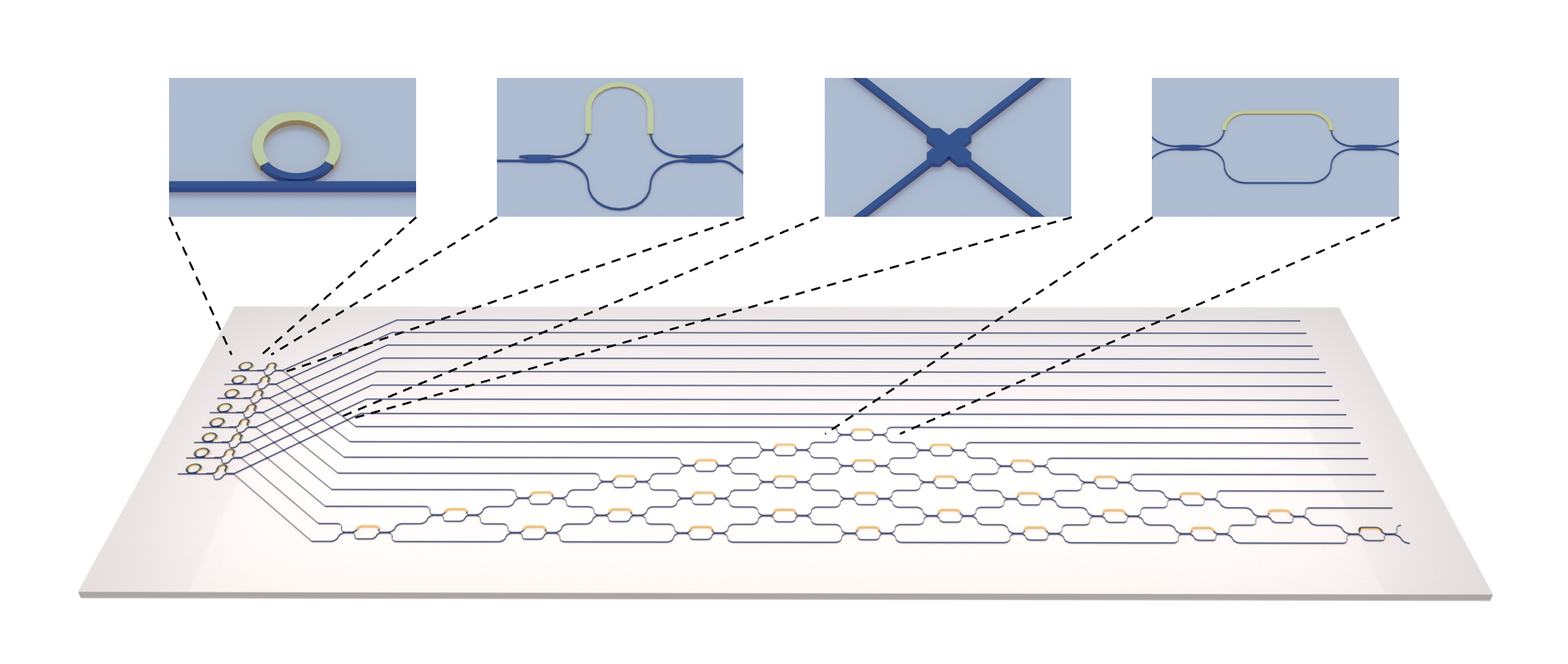
Because of its novelty, the AlGaAs platform has lacked the same level of individual circuit component development as more established platforms including silicon and silicon nitride. Here, we report on high-performance AlGaAsOI components including edge couplers, waveguide crossings, and tunable interferometers that, along with previously demonstrated ring resonator sources, form the foundation of a functional on-chip platform with potential not only in QPICs but classical PICs as well, including applications in optical communications and spectroscopyGaeta, Lipson, and Kippenberg (2019); Kippenberg et al. (2018); Spencer et al. (2018). Interferometers serve many purposes for on-chip optical quantum computing schemes including pump filtering, demultiplexing distinct frequency modes, acting as beamsplitters, and serving as linear optical quantum gates. Following the protocol proposed by Knill, Laflamme, and Milburn Knill, Laflamme, and Milburn (2001), scalable linear optical computing can be realized using only linear optical interferometers (reported here), single photon sources (shown in our previous manuscript Steiner et al. (2021)), and single-photon detectors (available commercially and also on-chipMcDonald et al. (2019)). Thus, with the design of high quality interferometers and low-loss chip-to-fiber couplers, the necessary components for many linear optical quantum computing protocols have been established. The other component discussed here–waveguide crossings–enables more complex circuit design where interactions between non-next nearest-neighbor qubits is necessary. Since the circuit elements are all fabricated using the same photonic layer, the routing requires waveguide crossings with minimal loss and crosstalk to adjacent channels. The development of these components opens the door for demonstrations of chip-scale QPICs using the AlGaAsOI platform, leveraging the benefits that AlGaAs offers over silicon and other nonlinear optical platformsChang et al. (2022). The components described below are designed assuming eventual full integration with AlGaAsOI ring resonator entangled-photon pair sources optimized for spontaneous four-wave mixing like that detailed in Ref. [(24)]. As an example, Fig. 1 shows a quantum photonic circuit for chip-scale Boson sampling to illustrate the opportunities that the development of interferometers and waveguide crossings can enable. The individual components are highlighted where they may reside in complex quantum photonic circuitry. In the remainder of this manuscript, we describe the design, simulation, and experimental results of many of the fundamental components to develop a quantum photonic platform.
II Quantum Photonic Toolbox
All of the components were fabricated using an AlGaAs photonic layer grown via molecular-beam epitaxy (MBE). The full fabrication procedure has been detailed previouslySteiner et al. (2021); Chang et al. (2020). Briefly, a GaAs chip with a 400-nm-thick AlGaAs photonic layer is bonded onto a 3-m-thick thermal SiO2 buffer layer on a Si substrate. After removing the substrate through selective wet etching, the AlGaAs surface is passivated using an 8-nm film of Al2O3 grown via atomic layer deposition (ALD). Deep ultraviolet photolithography is used to pattern photoresist, which is used to etch an SiO2 hardmask and then the AlGaAs photonic layer to define the components. Another ALD deposition of Al2O3 passivates the surface before a 1.0-m thick SiO2 cladding layer is deposited. Finally, 10 nm of titanium and 100 nm of platinum are deposited as resistive heaters for thermo-optic tuning.
II.1 Edge Couplers
Before a fully integrated QPIC is fabricated, it is necessary to utilize either fiber-based or free-space optical testing instruments. Thus, one of the first components to design is an efficient structure to couple light into and out of the photonic chip. Various strategies have been explored for efficient coupling Marchetti et al. (2019), but many of the methods that achieve ultra-high efficiency require additional fabrication steps, electron-beam lithography, anti-reflection coatings, or a full redesign of the input/output facet structure. For high throughput testing of individual components, much simpler structures can be used; as long as the fiber-to-chip coupling efficiency can be adequately characterized, any undesirable effects due to the input/output coupling can be isolated from the component performance.
There are two main categories of fiber-to-chip couplers: vertical couplers and edge couplers (also called "in-plane" or "butt" couplers, respectively). As the name suggests, vertical couplers accept incoming light from the top of the chip (out of plane) while edge couplers couple light impinging from one of the facets of the photonic chip (in plane). Depending on the desired application or testing design, there may be a benefit for utilizing either type of coupler. Vertical couplers are useful for more compact designs as they do not require waveguides to be routed completely to the edge of the photonic chipCheng et al. (2020). Generally, vertical couplers utilize periodic gratings that satisfy the Bragg condition in the waveguide to couple light into an optical fiber oriented almost perpendicularly to the surface Cheng et al. (2020); Taillaert et al. (2006). Edge couplers, on the other hand, can be much simpler to design and less sensitive to fabrication variation. Instead of relying on grating-based structures, edge couplers manipulate the waveguide dimensions to expand the waveguide mode to be closer matched with the mode in the fiberMu et al. (2020). The easiest way to achieve this conversion is to taper the waveguide to a narrow tip (called an "inverse taper") where the mode becomes weakly confined and expands closer to the mode size of the fiber. A standard taper, where the waveguide width is expanded at the facets, can also serve as an edge coupler. However, in high-index contrast platforms the design typically has lower efficiencies since the strongly confined mode will remain smaller than the fiber mode. The waveguide becomes capable of supporting multiple modes, and the high-index contrast produces large back reflectionsMu et al. (2020). Other edge coupling strategies include utilizing multiple inverse tapers in a trident or dual-tip design Liu and Yu (2007), polymer-based spot size converters Roelkens et al. (2005), or multi-layer spot size converters Fang et al. (2010). Due to the much simpler design, here we report only on inverse taper AlGaAsOI edge couplers. A scanning electron microscope image of several inverse tapers is shown in Fig. 2a). The facet is on the right side of the image, and the waveguides taper from 600 nm width (on the left) down to 200 nm at the facet. For a more in-depth study of the various types of coupling strategies, readers are referred to Ref. [(31)], which highlights various vertical and edge coupling strategies on the silicon-on-insulator (SOI) platform.
The inverse taper design reduces the confinement of the waveguide mode, increasing its effective modal area and decreasing its effective index of refraction. This allows for moderately high simulated coupling efficiencies (losses dB) to a (typically) lensed fiber aligned with the waveguide facet. The overall coupling loss is determined by effects such as reflection at the chip facet (due to refractive index mismatch), fiber-to-waveguide mode mismatch, and mode-conversion within the waveguide taper.
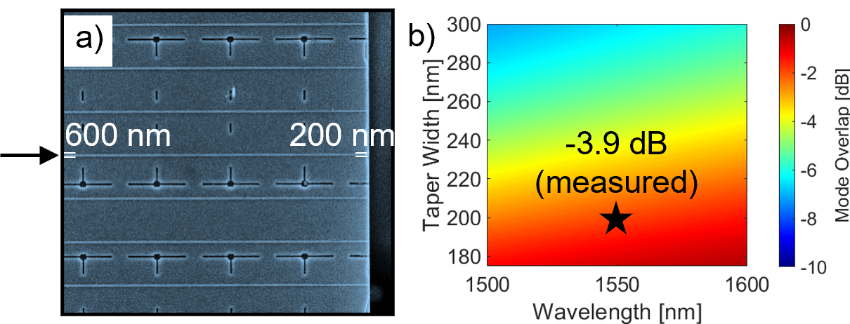
To determine the optimal design for an inverse taper edge coupler, the dimensions of the waveguide taper were varied and simulated using Lumerical Mode software. Here we only show the results for inverse tapers designed for the fundamental transverse electric (TE) mode because the components shown in the rest of this article are designed to operate with TE polarized light. Similar calculations can be made for the transverse magnetic (TM) mode. For a given Gaussian beam and waveguide geometry, the power overlap between the waveguide mode and fiber mode is calculated to estimate an upper bound on coupling efficiency and determine the optimum waveguide dimensions. This calculation does not include loss due to mode conversion or reflection at the interface. Figure 2b) illustrates the simulated mode overlap between a Gaussian beam with a mode field diameter of 2.5 (which matches the mode field diameter of commercially available lensed fibers) and a 400-nm thick AlGaAsOI waveguide with various taper widths. Narrow taper widths enlarge the waveguide mode to be nearly mode-matched with the incoming fiber mode, but the weak confinement of these narrow waveguides typically comes with additional loss as the light propagates through the narrow taper back to a waveguide width of 400 nm for the components. The fabrication of sub-200-nm features is challenging using the standard photolithography process, so we limit our taper designs to 200 nm or larger. Along with the simulated data, Fig. 2b) also shows a measured value for the coupling loss for a 200 nm edge coupler at a wavelength of 1550 nm. The measured value was collected by sending 10 dBm (10 mW) of light into a straight waveguide with 200 nm inverse tapers on the input and output facet. The collected power through the waveguide was 2.2 dBm, indicating an approximate loss of 3.9 dB/facet (the waveguide propagation loss is dB/cm and the waveguide is less than 2 mm, so the contributions of propagation loss are ignored in this measurement). The measured loss is larger than the simulated mode overlap, which is expected because the measurements also include reflections and mode conversion loss in the taper. The simulated mode overlap acts as an upper bound for the efficiency of the inverse taper. The 3.9 dB/facet of coupling loss in the AlGaAsOI platform is slightly larger than the sub-3 dB coupling loss expected from standard SOI inverse taper edge coupler designs Mu et al. (2020). The use of narrower taper widths (as shown in Fig. 2b)) or an anti-reflection coating will improve the coupling efficiency further, but ease of fabrication and reliability are prioritized, so for our initial devices, 200 nm inverse tapers are utilized.
II.2 Waveguide Crossings
Several methods have been explored for creating low-loss waveguide crossings including vertical coupling into polymer strip waveguides Tsarev (2011), multi-planar crossingsChiles et al. (2017), multimode interference-based crossingsChang and Zhang (2020); Bogaerts et al. (2007); Wu et al. (2020), and subwavelength gratingsBock et al. (2010). Many of these methods involve additional fabrication steps that can introduce excess loss and system design and fabrication challenges. A basic approach for a waveguide crossing relies on tapering an input single-mode waveguide section into a larger waveguide cross section that can support higher-order modes and relies on the beating between the fundamental mode and the higher-order mode to create an electric field maxima that is centered in the waveguide at the crossing location. By focusing the mode into the center of the wide waveguide, evanescent coupling to the perpendicular waveguide is minimized. This design can be completed with a basic linear taper (which will be referred to as a "simple crossing"), or a more complex structure. Here, we consider simulations of both simple and inverse-design crossings and report results from an inverse design approach (which will be referred to as a "13-width crossing") that utilizes 13 different widths in a parabolic taper that requires no additional fabrication steps and maintains low-loss and high-isolation transmission. This second design utilizes a swarm optimization protocol such that the optical mode is transmitted with minimal coupling to the crossed waveguide.
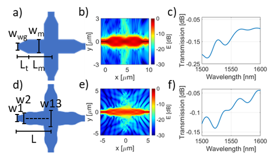
The simple crossing design is illustrated in Fig. 3a) and uses the beating between the fundamental and higher-order mode to create a confined optical mode centered at the location of the crossing. The beat length, , is defined as where are the propagation constants of the fundamental and first-order waveguide modes, respectively. For a 1.5 m multimode waveguide width (), the fundamental and first-order TE modes have effective indices of approximately 3.00 and 2.87, respectively, at a wavelength of 1550 nm. Using these effective indices, the beat length is calculated as 5.95 m. Finite difference time domain (FDTD) simulations were utilized to account for the transition region between the single-mode waveguide and the wider, multimode waveguide as well as allow for a larger bandwidth crossing to be designed where the average loss across a 100 nm bandwidth is utilized instead of maximizing at a single wavelength. The simulated mode profile for the simple crossing design and the simulated transmission through the device is shown in Fig. 3b,c), respectively. From the mode profile simulation, it is clear that the beating between the fundamental and higher order mode create a local maxima at the location of the crossing that minimizes the optical mode scattered into the perpendicularly oriented waveguide. The simulated loss through this structure is 0.15 dB at a wavelength of 1550 nm.
Figure 3d) shows the 13-width waveguide crossing with critical dimensions depicted. This design utilizes a swarm optimization protocol in an FDTD solver to optimize the transmission through the crossing by allowing the width to vary at 13 equally spaced sections along the taper. A parabolic interpolation between the 13 widths ensures a smooth transition between the various widths. The 13-width crossing design was also optimized for a bandwidth of 100 nm to maintain low-loss performance of the crossing across a broad bandwidth, which will be compatible with broadband entangled photon pair generation in quantum photonic circuits. Lower loss structures can be made when optimizing for a smaller bandwidth. Starting with an input waveguide width of 400 nm and total crossing length (L) of 9 m, the optimizer was allowed to vary the widths w2-w13 between 200 nm and 2000 nm. Figure 3e) shows the electric field profile for the optimal crossing design at a wavelength of 1550 nm, and Fig. 3f) plots the simulated transmission through the waveguide crossing as a function of the input wavelength. This crossing design has a simulated loss of approximately 0.1 dB at a wavelength of 1550 nm. Since the loss of the 13-width crossing design is smaller than the simple crossing design, the 13-width crossing was fabricated and tested initially.
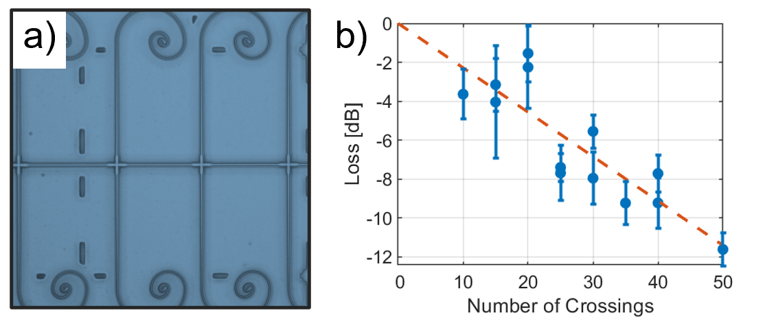
With the simulated waveguide crossing loss on the order of 0.1 dB, the cutback methodBogaerts et al. (2007) is used to measure the loss per crossing to remove coupling-dependent loss and reduce detector sensitivity limitations. For the 13-width crossing, waveguides with between 10 and 50 crossings were fabricated, and the loss through each line of crossings was measured across eight trials with complete re-alignment of the input and output fibers for each trial to remove any systematic variations due to coupling loss. Figure 4a) shows a microscope image of a few of the waveguide crossings in one of the lines. The vertical waveguide channels are terminated with tapered waveguides in a spiral geometry to prevent back-reflections into the crossing. The horizontal spacing of the crossings is varied randomly between 25 m and 35 m to avoid photonic cavity effects. Using the cutback method, the transmission through the crossings was measured at a wavelength of 1550 nm, and the results are shown in Fig. 4b). The dashed line indicates a linear fit of the loss as a function of the number of crossings, providing an estimated loss of dB/crossing. The error bars on the data points indicate the standard deviation of the eight independent measurement trials.
These results for the 13-width waveguide crossing (Fig. 3b) indicate that the fabricated crossings have slightly higher loss than the simulated loss at a wavelength of 1550 nm. This additional loss is likely due to fabrication variations in the widths along the device; the inverse design is more sensitive to fabrication variation than the use of a simple waveguide crossing. The measured dB of loss for the AlGaAsOI 13-width crossing is comparable to the dB of insertion loss reported from a genetic algorithm-designed SOI waveguide crossing Sanchis et al. (2009) and less than the loss of dB from silicon nitride waveguide crossings Yang et al. (2019). Other manuscripts report dB of insertion loss for elliptical tapers Fukazawa et al. (2004) and even on the order of dB for sub-wavelength grating-based structuresZhang et al. (2013). Ref. [(42)] compares various results of waveguide crossing on the SOI platform.
II.3 3 dB Couplers
Multimode Interferometers and Directional Couplers
A standard building block in both classical and quantum PICs is a 3-dB coupler. In QPICs, 3-dB couplers are utilized as their classical counterparts to distribute light evenly between two waveguides, to interfere single photons, and to serve as a component for tunable Mach-Zehnder Interferometers (MZIs) for programmable PICs. This places strict requirements on the devices, such as low loss for potential scalability, a large bandwidth to support broadband quantum light generation, and precise splitting ratios to maximize the extinction ratio and minimize cross-talk in MZIs. We explore two designs for creating on-chip 3-dB couplers: multimode interferometers (MMIs) and directional couplers (DCs). MMIs are based on the self-imaging principle, similar to the aforementioned simple waveguide crossings; however, unlike in the waveguide crossing design, the beat length between the two modes, , is used to calculate the core length necessary to achieve a splitting ratio as close to 3-dB as possible. The second coupler design based on DCs uses the overlap of evanescent modes between two neighboring waveguides, allowing the mode to fully couple into the adjacent waveguide. The full crossover length relies on the difference in refractive index between the even and odd supermodes created when two waveguides are in close proximity. DCs are straightforward couplers to design and are capable of any splitting ratio by adjusting the coupling length, but they are also more susceptible to fabrication imprecision and errors compared to MMIs.
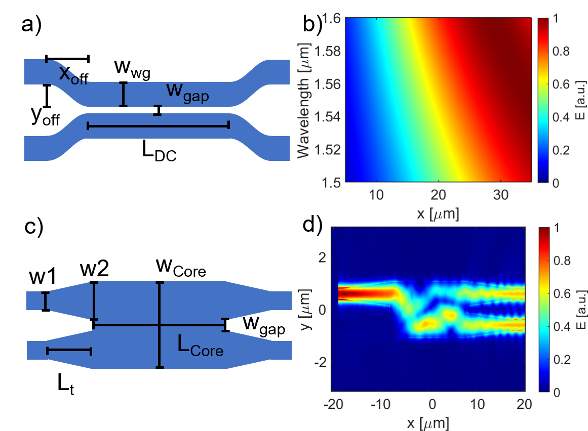
Figure 5 depicts two MMI and DC designs and results from FDTD simulations. For the MMIs, a core width of 2.1 m was selected. Because the self-imaging length scales with the MMI core width, a narrow width was chosen to reduce the component footprint. Symmetric input and output tapers expand the mode from a waveguide width of 0.4 m to 0.9 m nearest to the core. A 0.3 m separation leaves no excess core width beyond the dimensions of the tapers in an effort to reduce Fabry-Perot effects due to reflections. The core length design began by first calculating the beat length and multiplying it by a factor of 1.5, resulting in m. The full device was then simulated using FDTD, and the electric field profile is shown in Fig.5b). With a combination of the calculated beat length and FDTD simulations, a core length of 17.2 m was chosen. The 1.55 m difference between both methods is due to the input taper expanding the mode prior to reaching the MMI core not being considered during the beat-length calculation.
Unlike the MMIs, the DC design utilizes the same waveguide width, 0.4 m, across the entire device. Symmetric sine bend waveguides on the input and outputs with transverse displacements of 1.0 m and 8.0 m enable light to propagate near the coupling region. The minimum radius of these sine bends is kept to 20 m to reduce bending loss. The separation between the waveguides in the coupling region where the evanescent modal overlap occurs is 0.3 m. The coupling length for the full transfer of light from one waveguide to the other was first calculated with to give an estimate of the full crossover length of the mode, where is the effective indices of the even and odd supermodes that exist when the two waveguides are brought in close proximity. The finite difference eigenmode (FDE) results for the full crossover length is 48.47 m. Thus for a 3-dB coupler, m. A sweep of the coupling region using FDTD simulations of the full DC structure is depicted in Fig. 5d). The results of this simulation suggest an optimal 3-dB coupling length of 17.0 m. The difference between the two values is due to extra coupling effects in the sine bends. From the MZI measurements discussed in the next section, we can extract the performance of the couplers.
II.4 Mach-Zehnder Interferometers (MMI and DC)
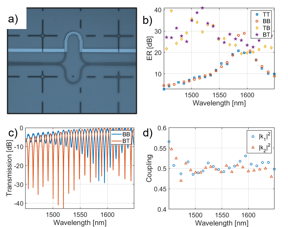
Tunable MZIs are a key component in QPICs by playing an important role for numerous functions, including as reconfigurable postselected entangling gates (R-PEGs)Adcock et al. (2018), demultiplexersHorst et al. (2013), variable beamsplittersWilkes et al. (2016), filtersPiekarek et al. (2016), and single photon quantum logic gatesAdcock et al. (2019). In an MZI, a 3-dB coupler splits light evenly into two different paths that may be equal (balanced MZI) or unequal (unbalanced MZI) in length, which then recombine with another coupler. Here, we focus on two variations of thermo-optically tunable unbalanced MZIs employing both DCs and MMIs. These devices were designed using the transfer matrix methodTran et al. (2016), where each component of the MZI can be represented by a matrix, two equivalent matrices for the 3-dB couplers, and a standalone matrix representing the path imbalance. Since many MZIs are required for a complete QPIC, the loss across each device must be minimized. Each coupler also should exhibit as close to a 3-dB splitting ratio as possible to achieve a maximum extinction ratio (ER), defined here as the power ratio of neighboring MZI fringes in the transmission spectrum.
Figure 6a) shows an optical image of an MZI utilizing DCs as couplers with a 30 m path imbalance on the top arm with the metal thermal tuner above the 1 m thick cladding to sweep and control the MZI phase. One advantage of thermo-optic tuning with AlGaAs is its inherent large thermo-optic coefficient, which, for an MZI with a 60 um path imbalance and a 10.28 nm free spectral range (FSR), allows for a full 2 phase sweep with 20 mW/ efficiency, which is 10 (0.6) times more efficient than silicon nitrideLee et al. (2022) (siliconLee et al. (2017)). The transmission spectrum of a 60 m path imbalance MZI with DC couplers is shown in Fig. 6b) for two different input/output configurations. The legend indicates which port light was coupled into and collected from, respectively, where T represents top and B represents bottom. The ER of all four ports are graphed in Fig. 6c). We typically observe an ER above 10 dB across nm bandwidth for through ports and nm for cross ports, comparable to silicon MZIsLee et al. (2019); Piekarek et al. (2016). With these ER measurements versus wavelength, the true coupling coefficient of each DC can be extractedTran et al. (2016), as shown in Fig. 6d). The DC couplers exhibit an average coupling coefficient of 0.5040.034 across a 100 nm bandwidth centered at 1570 nm.
III Qubit Demultiplexing
To benchmark our platform, we use a tunable MZI chip to demultiplex signal and idler photons generated from SFWM in a separate AlGaAsOI microring resonator chip previously reportedSteiner et al. (2021). The experimental setup schematic is shown in Figure 7a). The microring resonator temperature is stabilized with a thermo-electric cooler and control electronics. A tunable, narrow-linewidth continuous wave (cw) laser is tuned into resonance with a microresonator mode near 1557 nm. Tunable etalon-based bandpass filters are tuned to the pump wavelength and placed immediately after the laser to suppress amplified spontaneous emission at the wavelengths of the signal and idler modes, which helps improve the coincidence-to-accidental ratio in our experiments. The laser is polarized along the TE mode of the microresonator chip, and light is coupled onto the chip with high-numerical aperture lensed fiber. Pump light is coupled into the microring resonator using a critically coupled pulley coupler, where time-energy entangled signal and idler photon pairs are generated. The signal, idler, and pump photons are collected with a lensed fiber and then routed with polarization maintaining fiber to the MZI chip. When the phase of the MZI is properly tuned, it demultiplexes the signal and idler photons into separate waveguides. Light from one output port is coupled off chip using a lensed polarization-maintaining single-mode fiber. The output is then coupled to a 3-dB fiber beamsplitter, the output of which is demultiplexed with low-loss narrow-band filters and sent to superconducting nanowire single-photon detectors (SNSPDs) for coincidence detection.
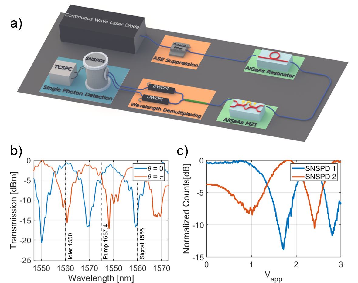
We chose to use an MMI-based MZI with a 60 m path imbalance for these experiments, despite the fact that its maximum ER is shifted away from 1550 nm due to the MMI design, because the FSR of this design most closely matches that of our microring resonator entangled-photon pair source. While the ER of this MZI is lower than that measured for the DC-based MZI, we show below that the performance of our demultiplexing experiment is at the maximum capability of our MZI based on its ER, demonstrating the promise of this platform for future all-on-chip demultiplexing. Figure 7b) shows the transmission spectrum of the MZI chip when coupling into and out of the top ports for two different thermo-optic heater voltages of 1 V and 1.8 V, which correspond to MZI phase 0 and radians, respectively, with an extinction ratio of 15 dB near the signal and idler wavelengths. As the phase is swept from 0 to , the transmission at a single wavelength sweeps from maximum to minimum. Vertical lines in the plot depict the wavelengths of the pump (1557.4 nm), signal (1565 nm), and idler (1550 nm) photons from our microring resonator. We next couple the entangled-photon pairs into the MZI for demultiplexing. Normalized counts from the two SNSPDs are shown in Fig. 7c) as a function of applied MZI voltage. We measure an extinction ratio of 14 dB near 1.65 V, which is comparable to the measured MZI extinction ratio shown in Fig. 7b). While these results are encouraging, we expect further improvements demultiplexing by improving the MMI splitting ratios to increase the demultiplexing ER and by designing an MZI with twice the FSR of the source.
IV Conclusion
Here we demonstrate many of the fundamental components necessary to develop fully integrated quantum photonic circuits on AlGaAsOI. With high-quality entangled photon pair sourcesSteiner et al. (2021) and the efficient edge couplers, 3 dB splitters, waveguide crossings, and MZIs demonstrated in this manuscript, a plethora of application-oriented integrated quantum circuits become available. Demonstrations of chip-to-chip quantum teleportationLlewellyn et al. (2019), multi-photon quantum information processing Adcock et al. (2019), and other large-scale quantum photonic circuits have already been realized on the SOI platformMoody et al. (2020); Lu et al. (2021). The benefits of the AlGaAsOI platform should enable more efficient demonstrations of these circuits at significantly lower optical pump power, reducing the required time to collect useful data and allowing for larger-scale circuits to be created. A summary of a few of the components discussed in this report is shown in Table 1 along with the performances of comparable components made on the SOI and Si3N4 platforms, which are also commonly used for quantum photonic circuits. It is important to note that the selected device performances were for Si and Si3N4 components that follow similar designs to the AlGaAsOI components that are relevant and routinely used for QPICs. For example, sub-edge couplers with 0.35 dB of loss have been fabricated using silicon with silicon nitride, but these were achieved with multiple layersWang et al. (2019). Here we compare similar component designs across the three platforms–using only a single photonic layer and standard photolithography to fabricate the devices. Overall, the AlGaAsOI components have similar or better performance to their SOI and Si3N4 counterparts, indicating that the transition to fully AlGaAsOI-based photonic circuits will have little to no degradation in performance compared to the current state-of-the-art platforms. Although the components detailed in this work were fabricated using a 22 mm by 24 mm bonded AlGaAs chip, wafer-scale bonding with compound-semiconductor-on-insulator is possibleStanton et al. (2020); Chang et al. (2022), enabling larger circuits to be created in the near future.
| AlGaAsOI | SOI | Si3N4 | |
| (this work) | |||
| Inverse Taper | dB | dBMu et al. (2020) | dBRamelow et al. (2015) |
| Coupling Loss | |||
| Waveguide Crossing | dB | dBSanchis et al. (2009) | dBYang et al. (2019) |
| Loss | |||
| MZI Extinction | dB | dBWang et al. (2016) | dBRao et al. (2021) |
| Ratio | |||
| MZI Bandwidth | nm Cross | nmLee et al. (2019) | nmRao et al. (2021) |
| ( dB ER) | nm Through | ||
| MZI Heater | 20 mW/ | mW/Lee et al. (2017) | mW/Lee et al. (2022) |
| Efficiency | (10.2 nm FSR) | (5.8 nm FSR) | (NA) |
Acknowledgements.
This work was supported by the NSF Quantum Foundry through Q-AMASE-i program Award No. DMR-1906325, AFOSR YIP Award No. FA9550-20-1-0150, and NSF Award CAREER-2045246. We also gratefully acknowledge support from the Cisco Research University Gift Program. T.J.S. and J.E.C. contributed equally to this work.Data Availability Statement
The data that support the findings in this study are available from the corresponding author upon reasonable request.
References
- Moody et al. (2020) G. Moody, L. Chang, T. J. Steiner, and J. E. Bowers, “Chip-Scale Nonlinear Photonics for Quantum Light Generation,” AVS Quantum Science 2, 041702 (2020).
- Vigliar et al. (2021) C. Vigliar, S. Paesani, Y. Ding, J. C. Adcock, J. Wang, S. Morley-Short, D. Bacco, L. K. Oxenløwe, M. G. Thompson, J. G. Rarity, and A. Laing, “Error-protected qubits in a silicon photonic chip,” Nature Physics 17, 1137–1143 (2021).
- Llewellyn et al. (2019) D. Llewellyn, Y. Ding, I. I. Faruque, S. Paesani, D. Bacco, R. Santagati, Y. J. Qian, Y. Li, Y. F. Xiao, M. Huber, M. Malik, G. F. Sinclair, X. Zhou, K. Rottwitt, J. L. O’Brien, J. G. Rarity, Q. Gong, L. K. Oxenlowe, J. Wang, and M. G. Thompson, “Chip-to-chip quantum teleportation and multi-photon entanglement in silicon,” Nature Physics 16, 148–153 (2019).
- Arrazola et al. (2021) J. M. Arrazola, V. Bergholm, K. Brádler, T. R. Bromley, M. J. Collins, I. Dhand, A. Fumagalli, T. Gerrits, A. Goussev, L. G. Helt, J. Hundal, T. Isacsson, R. B. Israel, J. Izaac, S. Jahangiri, R. Janik, N. Killoran, S. P. Kumar, J. Lavoie, A. E. Lita, D. H. Mahler, M. Menotti, B. Morrison, S. W. Nam, L. Neuhaus, H. Y. Qi, N. Quesada, A. Repingon, K. K. Sabapathy, M. Schuld, D. Su, J. Swinarton, A. Száva, K. Tan, P. Tan, V. D. Vaidya, Z. Vernon, Z. Zabaneh, and Y. Zhang, “Quantum circuits with many photons on a programmable nanophotonic chip,” Nature 591, 54–60 (2021).
- Zhao et al. (2020a) Y. Zhao, Y. Okawachi, J. K. Jang, X. Ji, M. Lipson, and A. L. Gaeta, “Near-Degenerate Quadrature-Squeezed Vacuum Generation on a Silicon-Nitride Chip,” Physical Review Letters 124, 193601 (2020a), 2002.01082 .
- Wang et al. (2018) J. Wang, S. Paesani, Y. Ding, R. Santagati, P. Skrzypczyk, A. Salavrakos, J. Tura, R. Augusiak, L. Mančinska, D. Bacco, D. Bonneau, J. W. Silverstone, Q. Gong, A. Acín, K. Rottwitt, L. K. Oxenløwe, J. L. O’Brien, A. Laing, and M. G. Thompson, “Multidimensional quantum entanglement with large-scale integrated optics,” Science 360, 285–291 (2018), 1803.04449 .
- Moody et al. (2022) G. Moody, V. J. Sorger, D. J. Blumenthal, P. W. Juodawlkis, W. Loh, C. Sorace-Agaskar, A. E. Jones, K. C. Balram, J. C. Matthews, A. Laing, et al., “2022 roadmap on integrated quantum photonics,” Journal of Physics: Photonics 4, 012501 (2022).
- Ma et al. (2017) C. Ma, X. Wang, V. Anant, A. D. Beyer, M. D. Shaw, and S. Mookherjea, “Silicon photonic entangled photon-pair and heralded single photon generation with car and g,” Optics Express 25, 32995–33006 (2017).
- Jaramillo-Villegas et al. (2017) J. A. Jaramillo-Villegas, P. Imany, O. D. Odele, D. E. Leaird, Z.-Y. Ou, M. Qi, and A. M. Weiner, “Persistent energy-time entanglement covering multiple resonances of an on-chip biphoton frequency comb,” Optica, Vol. 4, Issue 6, pp. 655-658 4, 655–658 (2017).
- Guo et al. (2016) X. Guo, C. L. Zou, C. Schuck, H. Jung, R. Cheng, and H. X. Tang, “Parametric down-conversion photon-pair source on a nanophotonic chip,” Light: Science & Applications 6, e16249–e16249 (2016).
- Zhao et al. (2020b) J. Zhao, C. Ma, M. Rüsing, and S. Mookherjea, “High quality entangled photon pair generation in periodically poled thin-film lithium niobate waveguides,” Physical Review Letters 124, 163603 (2020b).
- Boes et al. (2018) A. Boes, B. Corcoran, L. Chang, J. Bowers, and A. Mitchell, “Status and potential of lithium niobate on insulator (LNOI) for photonic integrated circuits,” Laser & Photonics Reviews 12, 1700256 (2018).
- Kumar et al. (2019) R. R. Kumar, M. Raevskaia, V. Pogoretskii, Y. Jiao, and H. K. Tsang, “Entangled photon pair generation from an inp membrane micro-ring resonator,” Applied Physics Letters 114, 021104 (2019).
- Xie et al. (2020) W. Xie, L. Chang, H. Shu, J. C. Norman, J. D. Peters, X. Wang, and J. E. Bowers, “Ultrahigh-q algaas-on-insulator microresonators for integrated nonlinear photonics,” Optics Express 28, 32894–32906 (2020).
- Ottaviano et al. (2016) L. Ottaviano, M. Pu, E. Semenova, and K. Yvind, “Low-loss high-confinement waveguides and microring resonators in AlGaAs-on-insulator,” Optics Letters 41, 3996–3999 (2016).
- Komma et al. (2012) J. Komma, C. Schwarz, G. Hofmann, D. Heinert, and R. Nawrodt, “Thermo-optic coefficient of silicon at 1550 nm and cryogenic temperatures,” Applied Physics Letters 101, 041905 (2012).
- Cocorullo, Corte, and Rendina (1999) G. Cocorullo, F. G. D. Corte, and I. Rendina, “Temperature dependence of the thermo-optic coefficient in crystalline silicon between room temperature and 550 k at the wavelength of 1523 nm,” Applied Physics Letters 74, 3338 (1999).
- Corte et al. (2000) F. G. D. Corte, G. Cocorullo, M. Iodice, and I. Rendina, “Temperature dependence of the thermo-optic coefficient of inp, gaas, and sic from room temperature to 600 k at the wavelength of 1.5 um,” Applied Physics Letters 77, 1614 (2000).
- Walker et al. (2019) R. Walker, N. Cameron, Y. Zhou, C. Main, G. Hoy, and S. Clements, “50ghz gallium arsenide electro-optic modulators for spaceborne telecommunications,” in International Conference on Space Optics — ICSO 2018, edited by N. Karafolas, Z. Sodnik, and B. Cugny (SPIE, 2019).
- Forsch et al. (2020) M. Forsch, R. Stockill, A. Walluck, I. Marinković, C. Gärtner, R. A. Norte, F. v. Otten, A. Fiore, K. Srinivasan, and S. Gröblacher, “Microwave-to-optics conversion using a mechanical oscillator in its quantum ground state.” Nature Physics 16, 69–74 (2020).
- Adachi (1994) S. Adachi, GaAs and Related Materials (WORLD SCIENTIFIC, 1994).
- Mariani et al. (2014) S. Mariani, A. Andronico, A. Lemaître, I. Favero, S. Ducci, and G. Leo, “Second-harmonic generation in algaas microdisks in the telecom range,” Optics Letters 39, 3062–3065 (2014).
- Chang et al. (2020) L. Chang, W. Xie, H. Shu, Q. F. Yang, B. Shen, A. Boes, J. D. Peters, W. Jin, C. Xiang, S. Liu, G. Moille, S. P. Yu, X. Wang, K. Srinivasan, S. B. Papp, K. Vahala, and J. E. Bowers, “Ultra-efficient frequency comb generation in algaas-on-insulator microresonators,” Nature Communications 11, 1–8 (2020).
- Steiner et al. (2021) T. J. Steiner, J. E. Castro, L. Chang, Q. Dang, W. Xie, J. Norman, J. E. Bowers, and G. Moody, “Ultrabright entangled-photon-pair generation from an algaas -on-insulator microring resonator,” PRX Quantum 2, 010337 (2021).
- Gaeta, Lipson, and Kippenberg (2019) A. L. Gaeta, M. Lipson, and T. J. Kippenberg, “Photonic-chip-based frequency combs,” Nature Photonics 2019 13:3 13, 158–169 (2019).
- Kippenberg et al. (2018) T. J. Kippenberg, A. L. Gaeta, M. Lipson, and M. L. Gorodetsky, “Dissipative kerr solitons in optical microresonators,” Science 361 (2018).
- Spencer et al. (2018) D. T. Spencer, T. Drake, T. C. Briles, J. Stone, L. C. Sinclair, C. Fredrick, Q. Li, D. Westly, B. R. Ilic, A. Bluestone, N. Volet, T. Komljenovic, L. Chang, S. H. Lee, D. Y. Oh, M. G. Suh, K. Y. Yang, M. H. Pfeiffer, T. J. Kippenberg, E. Norberg, L. Theogarajan, K. Vahala, N. R. Newbury, K. Srinivasan, J. E. Bowers, S. A. Diddams, and S. B. Papp, “An optical-frequency synthesizer using integrated photonics,” Nature 2018 557:7703 557, 81–85 (2018).
- Knill, Laflamme, and Milburn (2001) E. Knill, R. Laflamme, and G. J. Milburn, “A scheme for efficient quantum computation with linear optics,” Nature 409, 46–52 (2001).
- McDonald et al. (2019) C. McDonald, G. Moody, S. W. Nam, R. P. Mirin, J. M. Shainline, A. McCaughan, S. Buckley, and K. L. Silverman, “III-V photonic integrated circuit with waveguide-coupled light-emitting diodes and WSi superconducting single-photon detectors,” Applied Physics Letters 115, 081105 (2019).
- Chang et al. (2022) L. Chang, G. D. Cole, G. Moody, and J. E. Bowers, “Csoi: Beyond silicon-on-insulator photonics,” Optics and Photonics News 33, 24–31 (2022).
- Marchetti et al. (2019) R. Marchetti, C. Lacava, L. Carroll, K. Gradkowski, and P. Minzioni, “Coupling strategies for silicon photonics integrated chips [Invited],” Photonics Research 7, 201 (2019).
- Cheng et al. (2020) L. Cheng, S. Mao, Z. Li, Y. Han, and H. Y. Fu, “Grating couplers on silicon photonics: Design principles, emerging trends and practical issues,” Micromachines 11, 666 (2020).
- Taillaert et al. (2006) D. Taillaert, F. Van Laere, M. Ayre, W. Bogaerts, D. Van Thourhout, P. Bienstman, and R. Baets, “Grating couplers for coupling between optical fibers and nanophotonic waveguides,” Japanese Journal of Applied Physics, Part 1: Regular Papers and Short Notes and Review Papers 45, 6071–6077 (2006).
- Mu et al. (2020) X. Mu, S. Wu, L. Cheng, and H. Y. Fu, “Edge couplers in silicon photonic integrated circuits: A review,” Applied Sciences (Switzerland) 10, 1538 (2020).
- Liu and Yu (2007) Y. Liu and J. Yu, “Low-loss coupler between fiber and waveguide based on silicon-on-insulator slot waveguides,” Applied Optics 46, 7858–7861 (2007).
- Roelkens et al. (2005) G. Roelkens, P. Dumon, W. Bogaerts, D. van Thourhout, and R. Baets, “Efficient silicon-on-insulator fiber coupler fabricated using 248-nm-deep UV lithography,” IEEE Photonics Technology Letters 17, 2613–2615 (2005).
- Fang et al. (2010) Q. Fang, T.-Y. Liow, J. F. Song, C. W. Tan, M. B. Yu, G. Q. Lo, and D.-L. Kwong, “Suspended optical fiber-to-waveguide mode size converter for Silicon photonics,” Optics Express 18, 7763 (2010).
- Tsarev (2011) A. V. Tsarev, “Efficient silicon wire waveguide crossing with negligible loss and crosstalk,” Optics Express 19, 13732 (2011).
- Chiles et al. (2017) J. Chiles, S. Buckley, N. Nader, S. W. Nam, R. P. Mirin, and J. M. Shainline, “Multi-planar amorphous silicon photonics with compact interplanar couplers, cross talk mitigation, and low crossing loss,” APL Photonics 2, 116101 (2017).
- Chang and Zhang (2020) W. Chang and M. Zhang, “Silicon-based multimode waveguide crossings,” JPhys Photonics, 2, 022002 (2020).
- Bogaerts et al. (2007) W. Bogaerts, P. Dumon, D. V. Thourhout, and R. Baets, “Low-loss, low-cross-talk crossings for silicon-on-insulator nanophotonic waveguides,” Optics Letters 32, 2801 (2007).
- Wu et al. (2020) S. Wu, X. Mu, L. Cheng, S. Mao, and H. Y. Fu, “State-of-the-art and perspectives on silicon waveguide crossings: A review,” Micromachines 11, 326 (2020).
- Bock et al. (2010) P. J. Bock, P. Cheben, J. H. Schmid, J. Lapointe, A. Delâge, D.-X. Xu, S. Janz, A. Densmore, and T. J. Hall, “Subwavelength grating crossings for silicon wire waveguides,” Optics Express 18, 16146 (2010).
- Sanchis et al. (2009) P. Sanchis, P. Villalba, F. Cuesta, A. Håkansson, A. Griol, J. V. Galán, A. Brimont, and J. Martí, “Highly efficient crossing structure for silicon-on-insulator waveguides,” Optics Letters 34, 2760 (2009).
- Yang et al. (2019) H. Yang, P. Zheng, G. Hu, R. Zhang, B. Yun, and Y. Cui, “A broadband, low-crosstalk and low polarization dependent silicon nitride waveguide crossing based on the multimode-interference,” Optics Communications 450, 28–33 (2019).
- Fukazawa et al. (2004) T. Fukazawa, T. Hirano, F. Ohno, and T. Baba, “Low Loss Intersection of Si Photonic Wire Waveguides,” Japanese Journal of Applied Physics, Part 1: Regular Papers and Short Notes and Review Papers 43, 646–647 (2004).
- Zhang et al. (2013) Y. Zhang, A. Hosseini, X. Xu, D. Kwong, and R. T. Chen, “Ultralow-loss silicon waveguide crossing using Bloch modes in index-engineered cascaded multimode-interference couplers,” Optics Letters 38, 3608 (2013).
- Adcock et al. (2018) J. C. Adcock, S. Morley-Short, J. W. Silverstone, and M. G. Thompson, “Hard limits on the postselectability of optical graph states,” Quantum Science and Technology 4, 015010 (2018).
- Horst et al. (2013) F. Horst, W. M. Green, S. Assefa, S. M. Shank, Y. A. Vlasov, and B. J. Offrein, “Cascaded mach-zehnder wavelength filters in silicon photonics for low loss and flat pass-band wdm (de-)multiplexing,” Optics Express 21, 11652–11658 (2013).
- Wilkes et al. (2016) C. M. Wilkes, D. A. B. Miller, G. D. Marshall, J. Wang, J. L. O’Brien, M. G. Thompson, R. Santagati, S. Paesani, X. Qiang, and X. Zhou, “60-db high-extinction auto-configured mach–zehnder interferometer,” Optics Letters 41, 5318–5321 (2016).
- Piekarek et al. (2016) M. Piekarek, D. Bonneau, S. Miki, T. Yamashita, M. Fujiwara, M. Sasaki, H. Terai, M. G. Tanner, C. M. Natarajan, R. H. Hadfield, J. L. O’Brien, and M. G. Thompson, “Passive high-extinction integrated photonic filters for silicon quantum photonics,” Conference on Lasers and Electro-Optics , FM1N.6 (2016).
- Adcock et al. (2019) J. C. Adcock, C. Vigliar, R. Santagati, J. W. Silverstone, and M. G. Thompson, “Programmable four-photon graph states on a silicon chip,” Nature Communications 2019 10:1 10, 1–6 (2019).
- Tran et al. (2016) M. A. Tran, T. Komljenovic, J. C. Hulme, M. L. Davenport, and J. E. Bowers, “A robust method for characterization of optical waveguides and couplers,” IEEE Photonics Technology Letters 28, 1517–1520 (2016).
- Lee et al. (2022) J. M. Lee, W. J. Lee, M. S. Kim, S. W. Cho, J. J. Ju, G. Navickaite, and J. Fernandez, “Controlled-not operation of sin-photonic circuit using photon pairs from silicon-photonic circuit,” Optics Communications 509, 127863 (2022).
- Lee et al. (2017) J.-M. Lee, M.-S. Kim, J. T. Ahn, L. Adelmini, D. Fowler, C. Kopp, C. J. Oton, and F. Testa, “Demonstration and fabrication tolerance study of temperature-insensitive silicon-photonic MZI tunable by a metal heater,” J. Lightwave Technol. 35, 4903–4909 (2017).
- Lee et al. (2019) J. M. Lee, W. J. Lee, M. S. Kim, and J. J. Ju, “Noise filtering for highly correlated photon pairs from silicon waveguides,” Journal of Lightwave Technology 37, 5428–5434 (2019).
- Lu et al. (2021) L. Lu, X. Zheng, Y. Lu, S. Zhu, and X. S. Ma, “Advances in chip-scale quantum photonic technologies,” Advanced Quantum Technologies 4, 2100068 (2021).
- Wang et al. (2019) X. Wang, X. Quan, M. Liu, and X. Cheng, “Silicon-nitride-assisted edge coupler interfacing with high numerical aperture fiber,” IEEE Photonics Technology Letters 31, 349–352 (2019).
- Stanton et al. (2020) E. J. Stanton, J. Chiles, N. Nader, G. Moody, N. Volet, L. Chang, J. E. Bowers, S. Woo Nam, and R. P. Mirin, “Efficient second harmonic generation in nanophotonic GaAs-on-insulator waveguides,” Optics Express 28, 9521 (2020), 1912.12346 .
- Ramelow et al. (2015) S. Ramelow, A. Farsi, S. Clemmen, D. Orquiza, K. Luke, M. Lipson, and A. L. Gaeta, “Silicon-Nitride Platform for Narrowband Entangled Photon Generation,” (2015), arXiv:1508.04358 .
- Wang et al. (2016) J. Wang, D. Bonneau, M. Villa, J. W. Silverstone, R. Santagati, S. Miki, T. Yamashita, M. Fujiwara, M. Sasaki, H. Terai, M. G. Tanner, C. M. Natarajan, R. H. Hadfield, J. L. O’Brien, and M. G. Thompson, “Chip-to-chip quantum photonic interconnect by path-polarization interconversion,” Optica 3, 407–413 (2016).
- Rao et al. (2021) A. Rao, G. Moille, X. Lu, D. Westly, M. Geiselmann, M. Zervas, and K. Srinivasan, “Up to 50 db extinction in broadband single-stage thermo- optic mach-zehnder interferometers for programmable low-loss silicon nitride photonic circuits,” Conference on Lasers and Electro-Optics (2021), paper SM1A.7 , SM1A.7 (2021).