Calibration of Transition-edge Sensor (TES) bolometer arrays with application to CLASS
Abstract
The current and future cosmic microwave background (CMB) experiments fielding kilo-pixel arrays of transition-edge sensor (TES) bolometers require accurate and robust gain calibration methods. We simplify and refactor the standard TES model to directly relate the detector responsivity calibration and optical time constant to the measured TES current and the applied bias current . The calibration method developed for the Cosmology Large Angular Scale Surveyor (CLASS) TES bolometer arrays relies on current versus voltage (-) measurements acquired daily prior to CMB observations. By binning Q-band () - measurements by optical loading, we find that the gain calibration median standard error within a bin is 0.3%. We test the accuracy of this “- bin” detector calibration method by using the Moon as a photometric standard. The ratio of measured Moon amplitudes between the detector pairs sharing the same feedhorn indicates a TES calibration error of 0.5%. We also find that, for the CLASS Q-band TES array, calibrating the response of individual detectors based solely on the applied TES bias current accurately corrects TES gain variations across time but introduces a bias in the TES calibration from data counts to power units. Since the TES current bias value is set and recorded before every observation, this calibration method can always be applied to the raw TES data and is not subject to - data quality or processing errors.
tablenum \restoresymbolSIXtablenum
October 7, 2022
1 Introduction
Cosmic microwave background (CMB) observatories (Benson et al., 2014; Grayson et al., 2016; Gualtieri et al., 2018; Harrington et al., 2016; Suzuki et al., 2016; Lazear et al., 2014; Henderson et al., 2016) are mapping the sky with kilo-pixel arrays of transition-edge sensor (TES) detectors, and telescopes fielding even larger TES arrays will begin observing this decade (Ade et al., 2019; Abazajian et al., 2016; Sugai et al., 2020). Calibrating detector time-ordered data (TOD) to a standard unit is often the first step in processing astrophysical data sets. The calibration method must be accurate, to suppress systematic errors in the final results, and robust, to be applicable to a vast majority of observations. Data that cannot be calibrated are excluded, reducing the sensitivity of the instrument.
Current CMB telescopes operating TES bolometers have corrected for individual detector steady-state gain (i.e., DC gain) fluctuations using four methods based on: elevation nods (BICEP2 Collaboration et al., 2014), chopped thermal sources (Polarbear Collaboration et al., 2014; Sobrin et al., 2022), - data (i.e., load curves) (Dünner et al., 2013; Kusaka et al., 2018; BICEP2 Collaboration et al., 2014), and electrical bias step (Niemack, 2008; Rahlin, 2016; Filippini et al., 2022). The first two methods calibrate the TES gain to the brightness of an external source. Elevation nods measure the change in atmospheric emission with elevation, while chopped thermal sources are mounted in the telescope’s optical path and turned on/off on short time scales. These methods directly measure the optical response of the detectors but change the nominal observing state of the telescopes and thus use a portion of the observing time. Load curves measure the TES response to sweeping the bias voltage over a wide range, driving the TES from the normal state, to operating on transition, to superconducting. The bias step method drives small changes in TES bias current on top of the operating bias. Many experiments acquire - data before an observing run to choose the optimal operating bias for the detectors, with a run time of about one minute. Therefore, the - gain calibration is obtained from data already collected by the standard operation of the TES detectors. Bias steps may take only a few seconds and can be acquired during standard observations. These last two methods do not directly measure the optical response of the detectors, but infer it from the measured TES response to changes in bias current through our understanding of the TES bolometer electrothermal model. The novel - bin calibration method presented here combines daily load curve data across multiple observing years to improve the gain calibration for each day-long observing run. The improvement in gain calibration is achieved without decreasing the CMB observing efficiency. Future CMB space missions deploying TES bolometers (Sugai et al., 2020; Sutin et al., 2018) will likely rely on the Earth-velocity modulation of the CMB dipole as a gain calibrator (Bennett et al., 2003; Planck Collaboration et al., 2016a); nevertheless, their TES bolometer arrays may require periodic re-biasing based on load curves, providing an independent gain calibration method. The unique characteristics of any CMB telescope deploying TES bolometers combined with its observing strategy will determine which TES calibration methods are necessary to achieve the desired accuracy and control over systematic effects.
By mapping the polarization of the CMB over angular scales between 1 90∘, CLASS aims to test the paradigm of inflation (Guth, 1981; Sato, 1981; Linde, 1982; Starobinsky, 1982; Albrecht & Steinhardt, 1982; Planck Collaboration et al., 2020a) and probe the epoch of cosmic reionization (Hinshaw et al., 2013; Planck Collaboration et al., 2020b). The CLASS polarimeters measure the microwave sky in bands centered at approximately from an altitude of above sea level in the Atacama desert of northern Chile (Essinger-Hileman et al., 2014; Harrington et al., 2016) inside the Parque Astronómico Atacama (Bustos et al., 2014). The Q-band () telescope (Eimer et al., 2012; Appel et al., 2014) is sensitive to Galactic synchrotron emission, whereas the G-band (dichroic ) telescope (Dahal et al., 2020) is sensitive to Galactic dust emission. Two W-band () telescopes (Dahal et al., 2018) provide sensitivity to the CMB polarized signal near the Galactic foreground minimum 70 GHz (Bennett et al., 2013; Planck Collaboration et al., 2016b). The CLASS telescopes employ variable-delay polarization modulators (VPM) as their first optical element to increase stability and mitigate instrumental polarization (Miller et al., 2016; Chuss et al., 2012; Harrington et al., 2021). A co-moving ground shield limits terrestrial signal contamination. Telescope boresight rotation provides an additional level of sky signal polarization modulation by the instrument. The CLASS survey is forecast to constrain the optical depth to reionization to near the cosmic variance limit and the inflationary tensor-to-scalar ratio to (Watts et al., 2015, 2018). The optical depth is the least constrained CDM parameter, and new constraints from measurements at spherical-harmonic multipole moments are important for realizing the full potential of cosmological probes of neutrino masses (Allison et al., 2015; Watts et al., 2018).
This article describes the detector calibration method applied to the CLASS data. Section 2 presents the TES bolometer model used to interpret - data and extract detector responsivity calibration factors. Section 3 introduces a novel calibration method that leverages the many - data sets acquired over one or multiple observing years to optimize the calibration of each CMB scan set corresponding to a single - data set (each CLASS CMB scan set is approximately one day long). Section 4 discusses the detector calibration pipeline applied to CLASS data, from raw detector data to sky temperature units. It includes single detector calibration, relative calibration between detectors, gain corrections due to atmospheric opacity, and absolute calibration to CMB thermodynamic units. It also summarizes the various time scales of the experiment including: data rate, detector time constants, and calibration periods. Finally, Section 5 tests the validity and accuracy of the TES calibration methods considered in this paper by using observations of the Moon and the detector noise model as calibration references.
2 TES bolometer model
In this section, we develop a TES bolometer model (see Figure 1) based on the following assumptions:
-
1.
The TES operates at equilibrium with the power dissipated on the TES island matching the power transported by phonons from the island to the cold bath.
-
2.
The response of the TES electrical circuit is instantaneous compared to the TES thermal circuit (i.e., the low electrical-inductance limit).
Our aim is to model the TES with a negative feedback circuit (see Figure 3) and use it to extract TES parameters from - data. This approach circumvents solving the coupled differential equations describing the TES electrothermal circuit. Instead, we directly map the slope of - data to the TES zero-frequency responsivity.
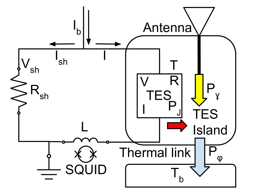
2.1 Bolometer power
A TES bolometer can be modeled as a coupled electrothermal system (Irwin & Hilton, 2005; Mather, 1982; Richards, 1994), as depicted in Figure 1. At equilibrium, the sum of the TES bias power () and optical signal () dissipated on the TES island equals the phonon power () that flows from the “hot” island to the “cold” bath through the silicon beam connecting them. This flow of power can be in the form of ballistic or diffuse phonons. The architecture and material properties of the CLASS bolometers (Rostem et al., 2014, 2016) imply ballistic phonons and hence power given by:
| (1) |
where , and is the thermal conductance constant set by the composition, geometry, and fabrication process of the beam (Rostem et al., 2014). is the bath temperature, while is the temperature of the device, which is restricted to a narrow range around the fiducial critical temperature , below which the resistance drops abruptly to zero. On the superconducting transition, the temperature is a function of TES resistance and TES current .111Unlike the more commonly used function , the function is single valued only on the superconducting transition. This is not limiting as all considerations herein concern functions on transition.
The thermal conductance () between the bolometer island and surrounding silicon frame is defined as
| (2) |
An - measurement consists of applying a high bias current () across the bolometer, heating the TES above its superconducting transition, and then decreasing the bias slowly (about 60 seconds from maximum to zero ). A typical - curve is shown in Figure 2. Initially, the TES current () decreases linearly with as expected for a normal resistor with resistance (i.e., the normal branch). At low enough , the TES island temperature decreases to , and the TES begins to function on its superconducting transition, where increases as decreases. On transition, the TES electrothermal feedback increases to maintain the equilibrium Joule power dissipation on the TES island as the voltage bias decreases with decreasing bias current. As approaches zero current, the equilibrium island temperature falls below , making the TES a superconducting short (i.e., the superconducting branch).
It is important to note that the SQUID readout measures changes in TES current () and not absolute TES current (). - curves are calibrated to absolute TES current units by linearly extrapolating the normal and/or superconducting branches and subtracting an offset to make these extrapolations go through the origin. Linearly extrapolating the normal branch section of the - that is far from the superconducting transition reduces the uncertainty on the offset. For CLASS -s, the median per-detector offset uncertainty is 0.4% (1-). Combining - data acquired under similar observing conditions further reduces the uncertainty on the absolute TES current calibration (see Section 3).
The TES resistance is connected in parallel with a shunt resistor (); hence, the TES DC voltage equals the shunt voltage , and the TES circuit splits into and (see circuit diagram in Figure 1). The electrical bias power dissipated on the TES () is obtained from:
| (3) |
The bias current is set by the user, and the TES current is measured from the calibrated -. The resistance of the shunt is measured by fitting a Johnson noise model to the noise spectra of the TES channel when the TES is in the superconducting state (i.e., zero bias current and ). We find that the measured shunt resistances for CLASS match the fabrication targets (see Table 1). The TES voltage bias circuit relates to and through
| (4) |
This relationship allows us to express as a function of the measured variables . It follows that can also be written in terms of and .
At equilibrium, the phonon power outflow equals the sum of the input electrical bias power and the optical power dissipated on the TES bolometer
| (5) |
is a combination of optical power coupled through the detector antennas in-band, out-of-band power that leaks through the band-defining on-chip filters, and stray light that reaches into the TES cavity and couples directly to the TES island. The CLASS detectors were designed to strongly suppress coupling to stray light and out-of-band optical power (Rostem et al., 2016; Crowe et al., 2013).
Before deploying each telescope, we conduct in-lab dark tests with the detector focal plane fully enclosed in a dark cavity (typically operating at ). Bolometer data acquired during dark tests satisfy the condition: , so that . The dark cavity radiates of optical power in the CLASS band and lower amounts at the higher-frequency CLASS bands. The dark cavity optical loading is negligible compared to the bias power () of the CLASS detectors (Dahal et al., 2022). is measured during observations by subtracting power (extracted from on-sky -s) from (deduced from dark -s), with both measured at the same 222Changes to the magnetic field environment near the TES between the lab and site configurations could lead to variations in that would introduce systematic errors to the measurements. Multiple layers of high-permeability Amumetal 4K (https://www.amuneal.com) in the CLASS cryostats suppress the ambient magnetic field by a factor of 100 (Ali, 2017), improving the accuracy of measurements from -s.. In lab with zero optical loading, Equation 1 can be used to fit for and by measuring at multiple temperatures below .
In an ideal TES, the superconducting transition vs is sharp and independent of . In this ideal case, the power conducted to the bath from a TES biased on transition is constant. The superconducting temperature of the CLASS TES depends weakly on and ; hence, decreases by a small amount as the detector is biased lower on the transition (Figure 2 shows as a function of ). It is then useful to consider, for each -, the value of measured high on the transition where and is near its minimum value. In particular for CLASS, we choose to define the TES saturation power as computed at . In dark tests (), can be interpreted as the maximum optical power that the TES island can absorb while maintaining its temperature on transition at .
2.2 Responsivity at the zero-frequency limit

During a single CMB observation schedule (1 day), a CLASS detector operates at the same and typically observes fluctuations on the order of a few percent of , driven primarily by changes in the opacity and temperature of the atmosphere. Therefore, we focus on calibrating small signals to the corresponding change in optical power dissipated on the TES island at a set . This calibration factor is called responsivity () and varies across detectors and/or observing conditions. The responsivity equation derived in Irwin & Hilton (2005) evaluated at the zero-frequency limit (i.e., DC responsivity) is
| (6) |
It depends on TES electrical time constant () and the TES loop gain () that typically require complex impedance measurements to constrain (Appel et al., 2009). is the TES loop inductance. The TES loop gain is defined as
| (7) |
and as
| (8) |
where , and .
Equation 6 can be expressed as
| (9) |
Below, we present an alternate approach to compute the TES DC responsivity (Appel, 2012) that relies on the slope and absolute calibration of - curves. In the following sections, references to “responsivity” refer to responsivity in the zero-frequency limit unless otherwise specified.
2.2.1 Ideal TES DC responsivity
Responsivity is defined as the change in TES current for a small change in . We can expand the latter as
| (10) | ||||
Under observing conditions, the bias current is constant . Therefore the inverse responsivity can be expressed as
| (11) |
In the ideal case where is approximately constant across the transition, the first term on the right hand side of Equation 11 is zero, and using Equation 3 to substitute for leads to
| (12) |
where denotes DC responsivity in the limit of an ideal TES where is constant across the transition. For the more general case where is not constant, we will show in Section 2.2.3 that the relevant contributions to the first term of Equation 11 can be estimated from the - curve measurement.
2.2.2 DC Responsivity
To apply a voltage bias across the TES, we require that , and hence . Therefore, a good approximation to Equation 12 is
| (13) |
where denotes the DC responsivity approximation in the limit where is constant across the transition and . Approximating responsivity through Equation 13 has the crucial advantage that it only depends on , a constant detector parameter, and , which is set to a known value at the beginning of every observing schedule. This responsivity estimate is independent of - information, so it is unaffected by missing or poor-quality - data. It provides a reference responsivity value that helps identify outlier responsivity values derived from - data, and provides a calibration factor of last resort when other methods fail. Applying to calibrate detector TODs has the drawback of introducing a gain bias factor (see Table 2) defined as
| (14) |
2.2.3 - DC Responsivity
For CLASS TES bolometers, changes across the transition since the TES temperature can vary slightly with TES current and TES resistance . The TES voltage bias circuit translates the dependence on into a function of and (see Equation 4).
For example, the - data plotted in Figure 2 shows decreasing with increasing . The detector optical loading is approximately constant during the - data acquisition, therefore . This means that the plotted - data also shows a decreasing with increasing when biased on transition. Since is not constant along the TES transition, the responsivity value calculated assuming the ideal case described by Equation 12 is only approximate.
Assuming is constant during the sweep of an - acquisition, then
| (15) |
| (16) |
and
| (17) |
Substituting equations 17 and 16 into 15, and dividing by yields
| (18) |
We can substitute Equation 18 for the first term on the right hand side of Equation 11 to obtain
| (19) |
By taking the partial derivative of Equation 1 with respect to , we arrive at
| (20) |
where we have used the relationship between and in Equation 4 to change the dependence back to the standard 333Note the simple chain rule expansion of the partial derivative is applicable as we are changing only one variable. Combining Equation 19 and Equation 20 yields
| (21) |
or, in terms of TES loop gain ,
| (22) |
Equation 22 places any dependence on into the measured - slope factor. By comparing Equation 9 to Equation 22, we find that the slope444At the operating TES bias current, the slope of the - curve is equivalent to the amplitude ratio of an applied bias current step over the TES current bias step response. Therefore, additional electrical bias step measurements can reduce the statistical uncertainty on the - responsivity estimate and/or provide an alternative method to measure responsivity on shorter time scales, as long as the TES absolute current is known. of the - data is related to the and parameters through
| (23) |
In the limit of (i.e., large ):
| (24) |
Four-wire measurements of CLASS TES MoAu bilayer show . During dark tests with , , hence Equation 7 is approximated by . The optical loading on the detectors, under typical observing condition from the CLASS site, reduces the Joule power by up to a half (), which implies . By employing Equation 24 to calculate the CLASS responsivity, we are introducing a bias of 4%. This is smaller than the 20% bias introduced by using or responsivity approximations (See in Table 2).
For the - responsivity model derived in this subsection, the gain bias defined by Equation 14 is
| (25) |
2.3 Detector time constant
Changes in the TES bolometer optical time constant () during sky observations can be tracked through - measurements. The bolometer thermal time constant () is the ratio of its heat capacity () to the thermal conductance () between the bolometer island and surrounding silicon frame. The TES electrical time constant () is always smaller than the ratio of the TES loop inductance () and the TES resistance () since . A typical CLASS TES operates with , much faster than the quickest thermal response (CLASS G-band array) . In this case, the electrothermal feedback loop created by voltage-biasing the TES can be considered to have infinite bandwidth, since . A feedback system as shown in Figure 3 with instantaneous feedback response (see Appendix A) speeds up by a factor:
| (26) |
where
| (27) |
| (28) |
In the limit of high loop gain (), Equation 26 allows us to compute the speed-up factor between the optical time constant and the TES thermal time constant from - data alone. Alternatively, we can constrain by combining - data with an independent measurements of 555 With the TES biased at the - inflection point where and , Equation 26 turns into At this bias setting high on the transition (Ullom & Bennett, 2015), and we can constrain by measuring with bias steps or other methods..
Using Equation 4 and Equation 23 to express Equation 26 in terms of , , and yields
| (29) |
| (30) |
This definition for matches the one presented in (Irwin & Hilton, 2005), and its interpretation as the detector optical time constant in the limit of low circuit inductance (i.e., instantaneous TES electrical circuit response).
While observing the sky, the typical CLASS TES optical time constant is around five times faster than the intrinsic detector thermal time constant (). In addition to correcting the detector gain by the TES DC responsivity, we divide out a single-pole transfer function that corrects changes in gain and phase across the signal band () due to the detector optical time constant. We obtain very accurate time constant measurements from analysing the VPM synchronous signal (VSS) (Harrington, 2018), which are cross-checked with the - derived time constant estimate described in this section. The detector time response is not a part of the DC calibration considered in Sections 4 and 5.
2.4 TES stability
The TES electrothermal feedback is stable as long as (Irwin & Hilton, 2005) or equivalently
| (31) |
As the detector is biased lower on the transition, this condition is harder to satisfy since decreases. To avoid TES instability, CLASS aims to operate all bolometers above 30% of . On the other hand, operating the TES lower on the transition has the benefit of suppressing detector Johnson noise through electrothermal feedback and reducing the noise contribution of the SQUID readout. The uniformity of the Q-band and G-band TES parameters (Chuss et al., 2016; Dahal et al., 2020) allows all detectors in these arrays to be biased between 30% and 60% . This has translated to optimized sensitivity and robust detector stability across a wide range of operating conditions. The variations across W-band detector wafers and the susceptibility of W-band TES to instability at higher % compared to the other arrays limit the number of W-band detectors biased on transition at the same time to 80% of the array (Dahal et al., 2022).
The CLASS Q-band TES film design later replicated in the W-band and G-band arrays was guided by estimates of the ratio of (or ) to extracted from - data (Appel et al., 2014). The chosen TES architecture typically operates with (see Table 2), and a ratio , therefore comfortably satisfying the stability condition of Equation 31.
2.5 CLASS TES model assumptions and approximations
Here we discuss the assumptions and approximations of the described TES bolometer model in the context of the CLASS detectors. We are interested in the TES operation at equilibrium, hence we focus on the detector DC responsivity and model the temporal response with a single-pole transfer function given by the optical time constant. We find this approach adequately captures the behaviour of the CLASS TES bolometers.
The CLASS detectors operate in the low-inductance limit and hence the electrical time constant is much faster than the thermal time constant. As noted in section 2.3 the electrical time constant is and the fastest CLASS thermal time constant is . Equation 9 indicates that the electrical-inductance of the TES circuit does not effect the TES DC responsivity, hence moving away from the low-inductance limit predominantly affects the temporal response of the TES.
The responsivity Equation 22 relies on making the linear approximations described by Equations 16 and 17, hence it is only valid on the small signal limit, where . For CLASS, this condition fails when observing bright sources like the Sun, or the Moon with the arrays, and when cloudy and/or high PWV atmospheric conditions appear at the site, in particular for the receiver.
For CLASS, we calculate the detector responsivity from Equation 24, which is a good approximation in the high limit. This is typically the case when the detectors operated in the middle-to-low resistance range of the TES transition. Detectors operating high on the transition () have low enough to introduce significant bias to the DC responsivity estimate.
When acquiring - data in the field, the optical signal is not perfectly constant. Typically, the atmospheric conditions do not change much during the one minute -, but during poor weather conditions the change can be significant. Additionally, we acquire -s with the telescope mount scanning and the VPM running. This means the - data is susceptible to the VPM synchronous signal (VSS). In the next section, we show that the - bin responsivity estimate helps average down the systematic error caused by superimposing the small VSS signal on the - data. This systematic error averages down because the phase of the VSS is random between different - data sets, and the VSS frequency is fast compared to the rate of change during the -.
3 - bin Calibration method
The set of all - measurements for each detector can be grouped into bins based on , which is a proxy for optical loading (). Analysis of -s grouped in the same bin yield similar detector parameters as long as the bin range is small. The CLASS Q-band - data sets are grouped in bins of 0.1 pW, while for W-band and G-band, the bin widths are 0.2 pW. These bin widths are only a few percent of the total detector .
All raw - data are calibrated to versus units and saved in a database indexed by detector number and . The mean and error estimate of a detector parameter (e.g., responsivity, time constant, etc) is extracted from the database by:
-
1.
finding the group of -s with values in the desired range;
-
2.
for all - in the group, computing the parameter value across a small range centered at the target ;
-
3.
eliminating outliers from the distribution of parameter results; and
-
4.
computing the mean and standard deviation of the distribution.
As observing time on the sky accumulates, more -s are acquired, which increases the number of measurements in each bin, leading to three advantages. First, it improves the precision of the parameter result per bin. Second, it allows for the recovery of detector parameters in the few instances the - acquisition failed, but the detector behaved properly during observations, by assuming the bias parameters of the otherwise-well-behaved detector are equal to bin averages. Third, it populates bins over a wide range of , revealing detector behavior beyond the standard small-signal TES bolometer model. Applying the - bin method to Q-band data acquired between June 2016 and August 2020 yields a responsivity median standard error of 0.3%.
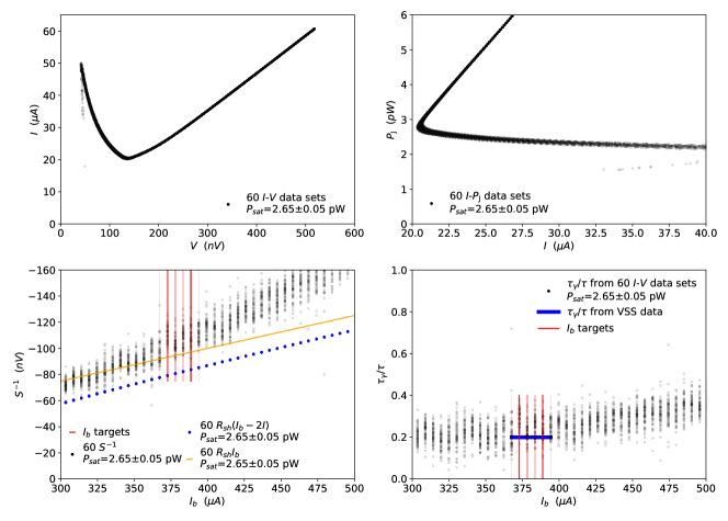
Figure 4 shows an example of this method, constraining a detector’s responsivity and time constant ratio in one bin across a range of targets.
4 CLASS detector calibration
Raw CLASS detector data are calibrated to thermodynamic CMB temperature units in five steps described in the following subsections: (1) The raw data are converted to TES current units, which allows the TES signal to be interpreted in the context of the TES model presented in Section 2. (2) The responsivity factor derived from the TES model transforms the measured TES current to optical power deposited at the bolometer. This step places on the same footing all the data of a single detector, accounting for any time-dependent variation related to the TES itself, such as changes in applied bias current or optical loading. (3) Apply gain calibration factors between detectors, thereby normalizing the data from the entire array of detectors to the same scale. These gain factors are equivalent to the relative optical efficiency between detectors. Any changes to detector optical efficiency over time (not captured by the responsivity calibration) can be incorporated at this step. (4) Apply a per-detector atmospheric opacity correction based on detector frequency band, elevation pointing, and precipitable water vapor (PWV) during the observation. The atmospheric opacity model is described in Section 4.4. (5) The array-normalized power is converted to thermodynamic temperature by calibrating off a bright Rayleigh–Jeans source such as the Moon (Appel et al., 2019; Xu et al., 2020) or a planet (Dahal et al., 2022), and applying a conversion factor from Rayleigh–Jeans temperature to CMB thermodynamic temperature based on the detector bandpass. Alternatively, this last calibration factor can be obtained from cross-correlating CLASS maps constructed in power units with Wilkinson Microwave Anisotropy Probe (WMAP; Bennett et al. 2013) and Planck (Planck Collaboration et al., 2020b) maps calibrated to CMB thermodynamic temperature.
In summary, a small signal of detector is calibrated to units through
| (33) |
where identifies the - used to compute the detector responsivity . Individual detector data are calibrated to array standard power through a relative detector gain factor . The atmospheric opacity gain correction is modeled for each detector at - time . The power to conversion factor is a single value for each array. Each term in Equation 33 is labeled from below with the section number discussing that calibration step.
4.1 Calibration to TES current
40 GHz 90 GHz 150 GHz 220 GHz () 5100 2100 2100 2100 () 1 1 1 1 14 14 14 14 24.6 24.6 24.6 24.6 2048 2048 2048 2048 () 573 573 573 573 () 5 5 5 5 15 15 15 15 () 250 250 200 200
The receiver data are recorded by a Multi-Channel Electronics (MCE) box developed at the University of British Columbia (Battistelli et al., 2008). The MCE records changes in the digital-to-analog (DAC) feedback () applied to the readout loop that nulls the signal of each channel. The TOD of this feedback signal represents the TES response to the sky signal. We first convert the TOD from raw DAC counts to TES current () through
| (34) |
where is the maximum voltage of the DAC, the resolution of the feedback DAC, the total resistance of the feedback circuit, the mutual inductance ratio between the TES and SQUID feedback coupling coils (Doriese et al., 2016), and the DC gain of the 4-pole Butterworth filter applied by the MCE before down-sampling to record the data at . The Butterworth filter is eventually divided out from the raw data to recover the TES response across the entire sampling bandwidth. Table 1 summarizes the CLASS MCE calibration parameter values.
The MCE applies the bias current () used to turn on the TES detectors. is calibrated from digital counts () to amperes through
| (35) |
where is the maximum voltage of the detector bias DAC, its resolution, and the total resistance of the detector bias circuit.
4.2 Calibration to power detected at the TES
40 GHz 90 GHz 150 GHz 220 GHz () (%) 24 (24) 24 26 45 (%) 13 (13) 24 21 25 1594 (2276) 1508 520 520 1.09 (1.09) 1.29 1.17 1.22 (%) 6 (6) 9 6 8 0.21 (0.20) 0.29 0.22 0.22 4.1 2.4 4.6 4.1 (%) 6 45 18 18 0.54 (0.43) 0.42 0.45 0.45 10.8 (13.8) 5.5 5.1 4.4 1.04 1.23 1.68 2.92
At the beginning of every observing schedule, typically once per day (Petroff et al., 2020), - data are acquired and analyzed to find the optimal detector bias voltage that will turn on and place all TES bolometers on their superconducting transition between 30% and 60% of their normal resistance (). From the applied bias current and this single - curve, we immediately generate responsivity calibration factors using Equation 24 that are applicable to the subsequent TOD sets. The statistical error of each responsivity estimate is reduced from 3.0% to 0.5% (see section 5 and Figure 6) by combining - data acquired between June 2016 and August 2020 under similar optical loading conditions as described in Section 3. We divide out a single-pole transfer function to correct for optical time constant gain and phase changes across the signal band. The detector optical time constants are measured from both the VPM synchronous signal and the detector - curves (see Section 2.3). Table 2 reports the average responsivity across each array, as well as the array 1- variance (), and the per-detector normalized (i.e., ) 1- variance (). Following Equation 14, we report the bias factor and 1- variance (), computed from the ratio of responsivity to - responsivity.
4.3 Gain calibration between detectors
To place all detector TODs on the same power scale, we divide the TES current signal by the - responsivity (Section 4.2) and divide by the relative calibration of detector . The relative calibration between detectors is constructed from high signal-to-noise measurements of the Moon and/or planets. The gain factors are equivalent to the relative optical efficiency of each detector, and by construction the mean of all across an array is equal to 1. With the TODs for all detectors in the array calibrated to the same power scale, the data can be combined to generate maps in standardized array power units. Table 2 reports the standard deviation of relative detector gains () across each array. Note that the statistical error on each detector extracted from point-source observations is ¡1%. The variations observed across the arrays are larger (%) than the per-detector measurement uncertainty.
4.4 Atmospheric opacity correction
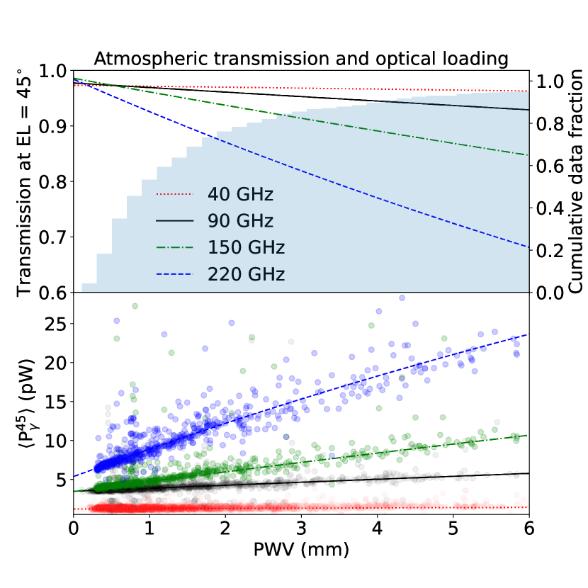
The opacity of the atmosphere along the line-of-sight suppresses the amplitude of the celestial sky signal. We apply an atmospheric opacity model based on Pardo et al. (2001) to correct the detector gain calibration across the four CLASS frequency bands. The opacity correction is a function of each detector’s elevation pointing, frequency bandpass, and the atmospheric PWV at the beginning of each scan. The PWV value input to the opacity model is either: (1) measured by nearby radiometers666Nearby radiometers include the UdeC and UCSC 183 GHz radiometer located at the Atacama Cosmology Telescope site (Bustos et al., 2014), and the Atacama Pathfinder Experiment radiometer (Güsten et al., 2006; Cortés et al., 2020), or (2) estimated from CLASS - optical loading measurements. Combining these two methods allows us to build a complete set of PWV values that encompasses all our CMB observations and to reject outliers by checking for consistency between the multiple PWV estimates. Figure 5 shows the transmission model for the four CLASS bands, the model’s predicted optical loading, and the - measured optical loading as a function of PWV. The model captures the dependence of the detector optical power on frequency band and PWV, increasing our confidence in the model’s atmospheric opacity correction. Note that at , the atmospheric transmission is nearly constant up to PWV, while the transmission drops by 30% at across the PWV range.
4.5 Calibration to CMB thermodynamic temperature
With the TODs of all detectors in the array calibrated to the same power standard, the entire data set can be co-added into one map. The final calibration step consists of converting this co-added map from power units to CMB thermodynamic temperature . This can be achieved by cross-correlating the map with WMAP or Planck maps. Alternatively, we can also estimate this absolute calibration factor from observations of the Moon (Appel et al., 2019; Xu et al., 2020) and planets (Dahal et al., 2022, 2021).
The power to conversion factor is a single value for each array where
| (36) |
and,
| (37) |
is Boltzmann’s constant, is Planck’s constant, is the CMB temperature of (Fixsen, 2009), the array average detector optical bandwidth, the array average bandpass center frequency, and the array average optical efficiency.
4.6 Observing and calibration time scales for CLASS
CLASS TES bolometer data is sampled every . The VPM completes a single modulation cycle every . The detector optical time constant is and is measured to high accuracy by tracking the phase of the VPM synchronous signal (Harrington, 2018). Corrections of the finite-time response of the detector, including variations in the detector time constant, are not part of the DC calibration described here and will be treated in future work. The nominal CLASS observing schedule is one day long, and it starts and ends with an - data acquisition. The opacity correction method described in section 4.4 is applied per observing schedule. We find this approach adequate at the lower CLASS frequency bands due to the relatively small change in atmospheric transmission with a typical change in PWV, but it may require further enhancement, especially for the band that is most sensitive to atmospheric water vapor fluctuations. We can track atmospheric opacity on shorter time scales by measuring the baseline drifts of the raw data (i.e., the intensity signal) and/or the changes in the VPM synchronous signal amplitude. Discussion of these methods is left for future publications.
- data gathered over a period of time where the detector focal plane configuration is unchanged can be grouped to generate an - bin calibration set. Changes to the telescope’s cryogenic receivers are rare, typically dividing observations into multi-year periods. Relative gain calibration periods coincide with changes to the cryogenic receiver or with changes to the optics, such as the addition of a thin-grill filter to the Q-band telescope window in 2019. Each subset of data with a relative calibration solution also has a corresponding absolute calibration to CMB thermodynamic temperature. A summary of the timescales of CLASS data is found in Table 3.
Time scale Data sampling rate VPM modulation period Detector optical time constant Detector thermal time constant CLASS CMB scan period - calibration period Atmosphere opacity correction - bin data sets Relative gain calibration between detectors Calibration to CMB temperature
5 CLASS calibration tests
This section discusses two tests of the CLASS TES responsivity model. The first test compiles 208 Moon scans acquired by the Q-band telescope between June 2016 and August 2020. These high signal-to-noise Moon measurements are used as a photometric standard to constrain the uncertainty of the responsivity models. The second test compares the expected Noise Equivalent Power (NEP) at each CLASS frequency band to the average measured NEP, applying - bin or calibration.
5.1 Q-band Moon photometric calibration test
To test the accuracy of the detector responsivity calibration, we would like to map a source with uniform brightness temperature across all observation runs. If the calibration method is accurate, the measured variations in the source’s brightness will be small.
The Moon is a good photometric calibration standard for the CLASS Q-band telescope because: (1) it is effectively a point source for the 1.5∘ full-width half max (FWHM) detector beam (Xu et al., 2020), (2) it drives a high signal-to-noise response without saturating the detectors, (3) its brightness temperature variations across time have been well characterized (Linsky, 1973; Krotikov & Pelyushenko, 1987; Zheng et al., 2012), and (4) the CLASS scanning strategy covering a large fraction of the sky leads to hundreds of Moon observations throughout the year.
A Moon antenna temperature model (Appel et al., 2019; Xu et al., 2020) is used to scale the measured Moon signal to a uniform standard. The Moon model accounts for angular diameter variation due to the Moon’s orbit and for surface temperature gradients caused by the Sun illuminating one side of the Moon (see Figure 2 in Xu et al. 2020).
The Moon antenna temperatures measured by each detector are computed using four different calibration methods: (1) - bin constructed by grouping - data based on optical loading (see Section 3), (2) - based on a single - acquired before the scan (see Section 2.2.3), (3) based on estimating responsivity from the applied detector bias current (see Equation 13), and (4) DAC based on applying no TES detector responsivity calibration.
For each calibration method, Table 4 presents the standard deviation of: (1) the per-detector normalized Moon amplitude (), (2) the normalized ratio of Moon amplitudes () between pairs of bolometers that share the same feedhorn divided by (to convert pair-ratio calibration uncertainty to per-detector uncertainty), (3) the detector responsivities across the array for the subset of - data associated to Moon observations (), and (4) the relative gain calibration between detectors (). Additionally, it includes the derived quantity obtained by subtracting in quadrature the estimated Moon model uncertainty of 1.5% from .
5.1.1 Variance of per-detector Moon amplitudes
The - bin calibration method reduces by nearly a factor of two compared to the standard - calibration. Therefore, the - bin calibration is more accurate, since its results are closer to the ideal scenario of the Moon as a perfect photometric standard ( = 0).
Applying the calibration results in a similar to the - bin calibration, we conjecture that this calibration method yields accurate results in the Moon photometric test because of the high uniformity of the Q-band observing conditions and detector properties. The - bin calibration is less susceptible to variation in the observing conditions but incorporates additional uncertainty from noise in the - data. Enhancing the quality of the - data would further improve the overall accuracy of both the - and - bin calibrations.
Each Moon measurement included in Figure 6 has high signal-to-noise, with statistical uncertainties . The variance of the distributions plotted on the top row are dominated by error in the Moon antenna temperature model and the per-detector calibration uncertainty across time.
5.1.2 Variance of detector pair-ratio Moon amplitudes
The normalized Moon pair-ratio amplitudes shown in the bottom-row plots of Figure 6 eliminate the uncertainty associated with the Moon antenna temperature model, since detector pairs measure the Moon at the same time (i.e., same Moon phase and angular diameter). Additionally, the detectors in each pair share the same bias line and are therefore biased by the same current, hence the ratios for the DAC and calibration are identical.
The - bin pair-ratio standard deviation indicates that the - bin responsivities add uncorrelated error to the calibration at the 0.5% level, comparable to the responsivity median standard error of 0.3% calculated from the distribution of responsivities values in - bins.
The small excess uncertainty may be attributed to: (1) additional error introduced by the beam-fitting algorithm used to extract the Moon amplitude. The Moon amplitude error of 0.2% is based on the variance of the Moon map away from the peak signal and does not include systematic uncertainty from fitting the model beam profile to the Moon map; (2) systematic error in the - bin responsivities not captured by the standard deviation in a bin; (3) error in the Moon model brightness temperature correction that persists in the pair ratio amplitudes due to systematic differences in the optical coupling of detector pairs.
5.1.3 Variance of per-detector Moon amplitudes corrected by the Moon model uncertainty
If we assume all - bin calibration errors are stochastic, then the primary source of uncertainty for the - bin and photometric calibration tests is a error introduced by the Moon antenna temperature model.
Subtracting the Moon model uncertainty from the - calibration yields a per-detector calibration uncertainty of , consistent with the per-detector calibration uncertainty estimated from the - pair-ratio result. The un-calibrated (DAC) per-detector variance corrected for the Moon model uncertainty (1-), indicates the level of detector gain variations across the selected Q-band Moon observations.
The DAC distribution of Moon pair-ratios indicates a 1- standard deviation of in the relative variation of detector responsivity between pairs, smaller than . This implies the per-detector gain variations are dominated by common-mode responsivity changes across pairs.
5.1.4 Variance of the detector array responsivities and the relative gain calibration between detectors
As expected, the per-detector DAC gain variations (= 3.1%) are similar to the variations in the per-detector responsivity values [- bin]. This variance of per-detector responsivities calculated for the subset of Moon observations considered in this photometric test is smaller than the reported in Table 2. The high signal-to-noise Moon observation sample used for the photometric test selects the best observing conditions and excludes poor-quality data from periods where changes in optical loading would drive greater variation in the TES responsivities. Also note that the per-detector gain variations across Moon observations are smaller than the differences in relative optical efficiency between detectors: , with - bin calibration applied (uncalibrated). Differences in the relative optical efficiencies are due to detector characteristics that are stable across time, such as the detector bandpass and location on the focal plane.
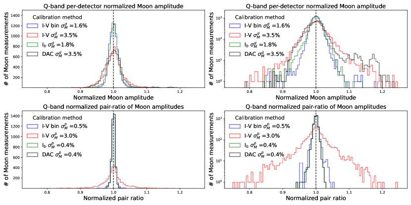
- bin - DAC (%) 1.6 3.5 1.8 3.5 (%) 0.5 3.0 0.4 0.4 (%) 0.5 3.1 1.0 3.1 (%) 3.3 4.4 3.0 NA (%) 6.5 6.4 7.0 16.6
5.2 NEP calibration test
By comparing the expected and measured noise amplitudes of detector data, we can test the accuracy of the detector calibration and identify possible systematic biases or excess noise sources.
The detector NEP is measured from TODs that are calibrated to power units through TES responsivity. The measured NEP values are compared to a robust TES NEP model based on measured detector bandpass and TES properties. Discrepancies between the average measured NEP and the NEP model can be attributed to excess noise sources or a responsivity calibration systematic error, particularly when the measured NEP falls below the model’s prediction. This comparison between modeled and measured NEP validates the - bin responsivity calibration and indicates that the responsivity is biased high.
The columns in Table 5 show the average NEP and for the four CLASS frequency bands. The NEP model average () is based on measured dark NEPs, Rayleigh–Jeans center frequencies, and bandwidths reported in (Dahal et al., 2022). is the average NEP computed using the responsivity calibration. is the average NEP computed using the - bin responsivity calibration. For all four bands, is lower than the theoretical lower limit set by , indicating a bias in the calibration method. is similar to or above . Excess NEP can be attributed to additional noise sources, such as instrument or atmospheric systematics.
40 GHz 90 GHz 150 GHz 220 GHz () 1.2 3.0 3.6 7.4 () 15.8 29.8 34.2 53.2 () 15.0 25.0 30.0 47.0 () 15.8 31.7 35.0 57.3
6 Conclusion
We introduced a TES model operating at equilibrium in the low electrical-inductance limit that allowed us to directly relate the detector responsivity calibration and optical time constant to the measured TES current and the applied bias current . A novel TES bolometer calibration method based on binning - data was applied to CLASS data acquired between June 2016 and August 2020, improving accuracy compared to single - calibration. This - bin calibration method can be applied to existing or future CMB data sets where many - measurements were acquired as part of the observing strategy.
We find that a simple TES calibration model based on the applied detector bias current yields precise per-detector TES power calibration factors for the CLASS Q-band array, but biases the absolute power calibration low. We conjecture that the observed high precision of the per-detector calibration is a result of the uniformity of the Q-band detector parameters and the relatively stable atmospheric emission at .
The atmospheric opacity model developed for the CLASS frequency bands reproduces the measured optical loading in each band as a function of PWV, corroborating the applied atmospheric gain correction model. We have described the calibration of CLASS TES bolometer data including factors normalizing for: 1) detector gain variations across time due to changes in optical loading and detector bias voltage; 2) optical efficiency variations across detectors; 3) changes in atmospheric opacity; and 4) an absolute temperature calibration based on Moon and planet observations.
The accuracy of the calibration pipeline is tested using Q-band Moon observations as a photometric standard and by comparing the measured detector noise versus NEP models at all four CLASS frequency bands.
The - bin calibration method yields a median per-detector TOD gain uncertainty of 0.3% in Q-band data, which is corroborated by using high signal-to-noise Moon observations as a photometric standard. The CLASS CMB data set is composed of thousands of day-long detector TODs; hence, we expect the demonstrated calibration uncertainty to contribute a negligible systematic error to the resulting maps and power spectra to be discussed in upcoming CLASS publications.
Appendix A Electrothermal speed-up factor
This appendix elaborates on the TES time constant speed-up factor attributed to the TES electrothermal feedback. It describes how to arrive at Equation 26 starting from the feedback circuit shown in Figure 7.
Consider the ratio of the output to input of the block diagram in Figure 7:
| (A1) |
The block diagram implies that and satisfy:
| (A2) |
Combining equations A1 and A2 to solve for , we arrive at
| (A3) |
Now consider to be the ratio of the output detector current to the input power and assuming a single-pole detector temporal response with effective time constant , then
| (A4) |
If the feedback loop is broken by removing , then the open loop response of is a single-pole transfer function set by the TES thermal time constant , where is the TES heat capacity and its thermal conductivity, therefore
| (A5) |
Typically, is a good assumption, where is an upper limit ( and ) on the TES electrical time constant (see Equation 8). is the TES circuit inductance and the TES resistance. In this low electrical-inductance limit, the electrothermal feedback has infinite bandwidth, and the transfer function of is a constant factor . Substituting equations A4 and A5 into A3, we obtain
| (A6) |
From Equation A6, we identify:
| (A7) |
hence arriving at Equation 26:
| (A8) |
Equation 26 can be expressed in terms of the ideal TES DC responsivity and responsivity by identifying and in the block diagram of Figure 3 as
| (A9) |
and
| (A10) |
Combining equations A8, A9, and A10 yields
| (A11) |
Equating the time constant ratio to the responsivity values allows us to quickly compute the electrothermal speed-up factor with the responsivity estimates already extracted from every - measurement.
References
- Abazajian et al. (2016) Abazajian, K. N., Adshead, P., Ahmed, Z., et al. 2016, arXiv e-prints, arXiv:1610.02743. https://arxiv.org/abs/1610.02743
- Ade et al. (2019) Ade, P., Aguirre, J., Ahmed, Z., et al. 2019, J. Cosmology Astropart. Phys, 2019, 056, doi: 10.1088/1475-7516/2019/02/056
- Albrecht & Steinhardt (1982) Albrecht, A., & Steinhardt, P. J. 1982, Physical Review Letters, 48, 1220, doi: 10.1103/PhysRevLett.48.1220
- Ali (2017) Ali, A. M. 2017, PhD thesis, Johns Hopkins University
- Allison et al. (2015) Allison, R., Caucal, P., Calabrese, E., Dunkley, J., & Louis, T. 2015, Phys. Rev. D, 92, 123535, doi: 10.1103/PhysRevD.92.123535
- Appel (2012) Appel, J. W. 2012, PhD thesis, Princeton University
- Appel et al. (2009) Appel, J. W., Austermann, J. E., Beall, J. A., et al. 2009, in American Institute of Physics Conference Series, Vol. 1185, The Thirteenth International Workshop on Low Temperature Detectors - LTD13, ed. B. Young, B. Cabrera, & A. Miller, 211–214, doi: 10.1063/1.3292317
- Appel et al. (2014) Appel, J. W., Ali, A., Amiri, M., et al. 2014, in Proc. SPIE, Vol. 9153, Millimeter, Submillimeter, and Far-Infrared Detectors and Instrumentation for Astronomy VII, 91531J, doi: 10.1117/12.2056530
- Appel et al. (2019) Appel, J. W., Xu, Z., Padilla, I. L., et al. 2019, ApJ, 876, 126, doi: 10.3847/1538-4357/ab1652
- Battistelli et al. (2008) Battistelli, E. S., Amiri, M., Burger, B., et al. 2008, Journal of Low Temperature Physics, 151, 908, doi: 10.1007/s10909-008-9772-z
- Bennett et al. (2003) Bennett, C. L., Halpern, M., Hinshaw, G., et al. 2003, ApJS, 148, 1, doi: 10.1086/377253
- Bennett et al. (2013) Bennett, C. L., Larson, D., Weiland, J. L., et al. 2013, ApJS, 208, 20, doi: 10.1088/0067-0049/208/2/20
- Benson et al. (2014) Benson, B. A., Ade, P. A. R., Ahmed, Z., et al. 2014, in Society of Photo-Optical Instrumentation Engineers (SPIE) Conference Series, Vol. 9153, Millimeter, Submillimeter, and Far-Infrared Detectors and Instrumentation for Astronomy VII, ed. W. S. Holland & J. Zmuidzinas, 91531P, doi: 10.1117/12.2057305
- BICEP2 Collaboration et al. (2014) BICEP2 Collaboration, Ade, P. A. R., Aikin, R. W., et al. 2014, ApJ, 792, 62, doi: 10.1088/0004-637X/792/1/62
- Bustos et al. (2014) Bustos, R., Rubio, M., Otárola, A., & Nagar, N. 2014, Publications of the Astronomical Society of the Pacific, 126, 1126, doi: 10.1086/679330
- Chuss et al. (2012) Chuss, D. T., Wollack, E. J., Henry, R., et al. 2012, Appl. Opt., 51, 197, doi: 10.1364/AO.51.000197
- Chuss et al. (2016) Chuss, D. T., Ali, A., Amiri, M., et al. 2016, Journal of Low Temperature Physics, 184, 759, doi: 10.1007/s10909-015-1368-9
- Cortés et al. (2020) Cortés, F., Cortés, K., Reeves, R., Bustos, R., & Radford, S. 2020, A&A, 640, A126, doi: 10.1051/0004-6361/202037784
- Crowe et al. (2013) Crowe, E. J., Bennett, C. L., Chuss, D. T., et al. 2013, IEEE Transactions on Applied Superconductivity, 23, 2500505, doi: 10.1109/TASC.2012.2237211
- Dahal et al. (2018) Dahal, S., Ali, A., Appel, J. W., et al. 2018, in Society of Photo-Optical Instrumentation Engineers (SPIE) Conference Series, Vol. 10708, Millimeter, Submillimeter, and Far-Infrared Detectors and Instrumentation for Astronomy IX, ed. J. Zmuidzinas & J.-R. Gao, 107081Y, doi: 10.1117/12.2311812
- Dahal et al. (2020) Dahal, S., Amiri, M., Appel, J. W., et al. 2020, Journal of Low Temperature Physics, 199, 289, doi: 10.1007/s10909-019-02317-0
- Dahal et al. (2021) Dahal, S., Brewer, M. K., Appel, J. W., et al. 2021, The Planetary Science Journal, 2, 71, doi: 10.3847/PSJ/abedad
- Dahal et al. (2022) Dahal, S., Appel, J. W., Datta, R., et al. 2022, ApJ, 926, 33, doi: 10.3847/1538-4357/ac397c
- Doriese et al. (2016) Doriese, W. B., Morgan, K. M., Bennett, D. A., et al. 2016, Journal of Low Temperature Physics, 184, 389, doi: 10.1007/s10909-015-1373-z
- Dünner et al. (2013) Dünner, R., Hasselfield, M., Marriage, T. A., et al. 2013, ApJ, 762, 10, doi: 10.1088/0004-637X/762/1/10
- Eimer et al. (2012) Eimer, J. R., Bennett, C. L., Chuss, D. T., et al. 2012, in Society of Photo-Optical Instrumentation Engineers (SPIE) Conference Series, Vol. 8452, Millimeter, Submillimeter, and Far-Infrared Detectors and Instrumentation for Astronomy VI, ed. W. S. Holland & J. Zmuidzinas, 845220, doi: 10.1117/12.925464
- Essinger-Hileman et al. (2014) Essinger-Hileman, T., Ali, A., Amiri, M., et al. 2014, in SPIE, Vol. 915354, Millimeter, Submillimeter, and Far-Infrared Detectors and Instrumentation for Astronomy VII
- Filippini et al. (2022) Filippini, J. P., Gambrel, A. E., Rahlin, A. S., et al. 2022, Journal of Low Temperature Physics, doi: 10.1007/s10909-022-02729-5
- Fixsen (2009) Fixsen, D. J. 2009, ApJ, 707, 916. http://stacks.iop.org/0004-637X/707/i=2/a=916
- Grayson et al. (2016) Grayson, J. A., Ade, P. A. R., Ahmed, Z., et al. 2016, in Society of Photo-Optical Instrumentation Engineers (SPIE) Conference Series, Vol. 9914, Millimeter, Submillimeter, and Far-Infrared Detectors and Instrumentation for Astronomy VIII, ed. W. S. Holland & J. Zmuidzinas, 99140S, doi: 10.1117/12.2233894
- Gualtieri et al. (2018) Gualtieri, R., Filippini, J. P., Ade, P. A. R., et al. 2018, Journal of Low Temperature Physics, 193, 1112, doi: 10.1007/s10909-018-2078-x
- Güsten et al. (2006) Güsten, R., Nyman, L. Å., Schilke, P., et al. 2006, A&A, 454, L13, doi: 10.1051/0004-6361:20065420
- Guth (1981) Guth, A. H. 1981, Phys. Rev. D, 23, 347, doi: 10.1103/PhysRevD.23.347
- Harrington et al. (2016) Harrington, K., Marriage, T., Ali, A., et al. 2016, in Society of Photo-Optical Instrumentation Engineers (SPIE) Conference Series, Vol. 9914, Millimeter, Submillimeter, and Far-Infrared Detectors and Instrumentation for Astronomy VIII, ed. W. S. Holland & J. Zmuidzinas, 99141K, doi: 10.1117/12.2233125
- Harrington et al. (2021) Harrington, K., Datta, R., Osumi, K., et al. 2021, ApJ, 922, 212, doi: 10.3847/1538-4357/ac2235
- Harrington (2018) Harrington, K. M. 2018, PhD thesis, Johns Hopkins University
- Harris et al. (2020) Harris, C. R., Millman, K. J., van der Walt, S. J., et al. 2020, Nature, 585, 357, doi: 10.1038/s41586-020-2649-2
- Henderson et al. (2016) Henderson, S. W., Allison, R., Austermann, J., et al. 2016, Journal of Low Temperature Physics, 184, 772, doi: 10.1007/s10909-016-1575-z
- Hinshaw et al. (2013) Hinshaw, G., Larson, D., Komatsu, E., et al. 2013, ApJS, 208, 19, doi: 10.1088/0067-0049/208/2/19
- Hunter (2007) Hunter, J. D. 2007, Computing in Science Engineering, 9, 90, doi: 10.1109/MCSE.2007.55
- Irwin & Hilton (2005) Irwin, K., & Hilton, G. 2005, in Topics in Applied Physics, Vol. 99, Cryogenic Particle Detection, ed. C. Enss (Springer Berlin / Heidelberg), 81–97
- Krotikov & Pelyushenko (1987) Krotikov, V. D., & Pelyushenko, S. A. 1987, Soviet Ast., 31, 216
- Kusaka et al. (2018) Kusaka, A., Appel, J., Essinger-Hileman, T., et al. 2018, J. Cosmology Astropart. Phys, 2018, 005, doi: 10.1088/1475-7516/2018/09/005
- Lazear et al. (2014) Lazear, J., Ade, P., Benford, D. J., et al. 2014, in American Astronomical Society Meeting Abstracts, Vol. 223, American Astronomical Society Meeting Abstracts, 439.02
- Linde (1982) Linde, A. D. 1982, Physics Letters B, 108, 389, doi: 10.1016/0370-2693(82)91219-9
- Linsky (1973) Linsky, J. L. 1973, ApJS, 25, 163, doi: 10.1086/190266
- Mather (1982) Mather, J. C. 1982, Appl. Opt., 21, 1125, doi: 10.1364/AO.21.001125
- Miller et al. (2016) Miller, N. J., Chuss, D. T., Marriage, T. A., et al. 2016, ApJ, 818, 151, doi: 10.3847/0004-637X/818/2/151
- Niemack (2008) Niemack, M. D. 2008, PhD thesis, Princeton University
- Pardo et al. (2001) Pardo, J. R., Cernicharo, J., & Serabyn, E. 2001, IEEE Transactions on Antennas and Propagation, 49, 1683, doi: 10.1109/8.982447
- Petroff et al. (2020) Petroff, M. A., Appel, J. W., Bennett, C. L., et al. 2020, in Society of Photo-Optical Instrumentation Engineers (SPIE) Conference Series, Vol. 11452, Society of Photo-Optical Instrumentation Engineers (SPIE) Conference Series, 114521O, doi: 10.1117/12.2561609
- Planck Collaboration et al. (2016a) Planck Collaboration, Adam, R., Ade, P. A. R., et al. 2016a, A&A, 594, A8, doi: 10.1051/0004-6361/201525820
- Planck Collaboration et al. (2016b) —. 2016b, A&A, 594, A10, doi: 10.1051/0004-6361/201525967
- Planck Collaboration et al. (2020a) Planck Collaboration, Akrami, Y., Arroja, F., et al. 2020a, A&A, 641, A10, doi: 10.1051/0004-6361/201833887
- Planck Collaboration et al. (2020b) Planck Collaboration, Aghanim, N., Akrami, Y., et al. 2020b, A&A, 641, A6, doi: 10.1051/0004-6361/201833910
- Polarbear Collaboration et al. (2014) Polarbear Collaboration, Ade, P. A. R., Akiba, Y., et al. 2014, ApJ, 794, 171, doi: 10.1088/0004-637X/794/2/171
- Rahlin (2016) Rahlin, A. S. 2016, PhD thesis, Princeton University
- Richards (1994) Richards, P. L. 1994, Journal of Applied Physics, 76, 1, doi: 10.1063/1.357128
- Rostem et al. (2014) Rostem, K., Chuss, D. T., Colazo, F. A., et al. 2014, Journal of Applied Physics, 115, 124508, doi: 10.1063/1.4869737
- Rostem et al. (2016) Rostem, K., Ali, A., Appel, J. W., et al. 2016, in Society of Photo-Optical Instrumentation Engineers (SPIE) Conference Series, Vol. 9914, Millimeter, Submillimeter, and Far-Infrared Detectors and Instrumentation for Astronomy VIII, ed. W. S. Holland & J. Zmuidzinas, 99140D, doi: 10.1117/12.2234308
- Sato (1981) Sato, K. 1981, MNRAS, 195, 467
- Sobrin et al. (2022) Sobrin, J. A., Anderson, A. J., Bender, A. N., et al. 2022, ApJS, 258, 42, doi: 10.3847/1538-4365/ac374f
- Starobinsky (1982) Starobinsky, A. A. 1982, Physics Letters B, 117, 175, doi: 10.1016/0370-2693(82)90541-X
- Sugai et al. (2020) Sugai, H., Ade, P. A. R., Akiba, Y., et al. 2020, Journal of Low Temperature Physics, 199, 1107, doi: 10.1007/s10909-019-02329-w
- Sutin et al. (2018) Sutin, B. M., Alvarez, M., Battaglia, N., et al. 2018, in Society of Photo-Optical Instrumentation Engineers (SPIE) Conference Series, Vol. 10698, Space Telescopes and Instrumentation 2018: Optical, Infrared, and Millimeter Wave, ed. M. Lystrup, H. A. MacEwen, G. G. Fazio, N. Batalha, N. Siegler, & E. C. Tong, 106984F, doi: 10.1117/12.2311326
- Suzuki et al. (2016) Suzuki, A., Ade, P., Akiba, Y., et al. 2016, Journal of Low Temperature Physics, 184, 805, doi: 10.1007/s10909-015-1425-4
- Ullom & Bennett (2015) Ullom, J. N., & Bennett, D. A. 2015, Superconductor Science Technology, 28, 084003, doi: 10.1088/0953-2048/28/8/084003
- Virtanen et al. (2020) Virtanen, P., Gommers, R., Oliphant, T. E., et al. 2020, Nature Methods, 17, 261, doi: 10.1038/s41592-019-0686-2
- Watts et al. (2015) Watts, D. J., Larson, D., Marriage, T. A., et al. 2015, ApJ, 814, 103, doi: 10.1088/0004-637X/814/2/103
- Watts et al. (2018) Watts, D. J., Wang, B., Ali, A., et al. 2018, ApJ, 863, 121. http://stacks.iop.org/0004-637X/863/i=2/a=121
- Xu et al. (2020) Xu, Z., Brewer, M. K., Rojas, P. F., et al. 2020, ApJ, 891, 134, doi: 10.3847/1538-4357/ab76c2
- Zheng et al. (2012) Zheng, Y. C., Tsang, K. T., Chan, K. L., et al. 2012, Icarus, 219, 194, doi: 10.1016/j.icarus.2012.02.017