Plateau Regions for Zero-Bias Peaks within 5 of the Quantized Conductance Value
Abstract
Probing an isolated Majorana zero mode is predicted to reveal a tunneling conductance quantized at at zero temperature. Experimentally, a zero-bias peak (ZBP) is expected and its height should remain robust against relevant parameter tuning, forming a quantized plateau. Here, we report the observation of large ZBPs in a thin InAs-Al hybrid nanowire device. The ZBP height can stick close to , mostly within tolerance, by sweeping gate voltages and magnetic field. We further map out the phase diagram and identify two plateau regions in the phase space. Despite the presence of disorder and quantum dots, our result constitutes a step forward towards establishing Majorana zero modes.
Majorana zero modes (MZMs) [1, 2] have been extensively searched in hybrid semiconductor-superconductor nanowire devices since the first material prediction in 2010 [3, 4]. One key prediction, a quantized zero bias peak (ZBP) in tunneling conductance [5, 6, 7, 8], still remains illusive so far [9, 10, 11, 12, 13, 14, 15, 16]. Moreover, theory developments have proposed the concept of quasi-MZMs due to smooth potential variation [17, 18, 19, 20, 21, 22, 23] or disorder [24, 25, 26, 27, 28, 29]. These quasi-MZMs, though topologically trivial, can also lead to quantized ZBPs. The quantization mechanisms for MZMs and quasi-MZMs are similar: the conductance is solely contributed by one isolated MZM while the second MZM is decoupled. Recent experimental progress has reported large ZBPs whose height can reach [13, 14]. However, a single peak at is not enough to be entitled as ‘quantized’. A quantized ZBP requires the peak height sticking to by tuning all relevant experimental knobs: a plateau defined by parameter sweepings. This plateau phenomenon is still missing in experiments.
Here, we have improved the device fabrication and report ZBPs near , forming a plateau defined by sweeping gate voltages and magnetic field () in an ultra-thin InAs-Al nanowire device. We quantify the plateau with a tolerance of , a number commonly used in recent literature [26, 27]. In the end, we discuss their possible connections to MZMs or quasi-MZMs.
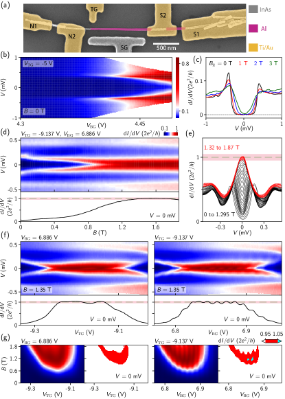
Figure 1a shows the device scanning electron micrograph (SEM). Material and growth details can be found in Ref [30]. The InAs diameter ( 26 nm) is much thinner than those commonly used ( 100 nm), aiming for fewer subband occupations. Theory has shown that fewer or single subband regime is preferred for MZM quantization [18, 31, 32]. The device was measured in a dilution fridge, base temperature 20 mK. The electron can be below 40 mK. A total bias voltage together with a lock-in excitation was applied to contact N1 with the current and drained from S1. A voltage meter measured and between N2 and S2. This four-terminal set-up can exclude the contributions of contact resistance as a systematic uncertainty. The tunnel gate (TG) and back gate (BG) were used while SG was not well functional and kept grounded. See Fig. S1 for circuit details.
The tunneling spectroscopy at zero (Fig. 1b) resolves a hard superconducting gap. The gap size is 0.39 mV due to the thin Al film. Fig. 1c shows the dependence of the gap. The z axis is 8∘ misaligned with the nanowire. For along other directions, see Fig. S2. The gap remains hard below 2 T and gradually becomes soft above 3 T. Hard gap at high is necessary for MZM quantization since a soft gap destroys the quantization by dissipation [33, 34].
In Fig. 1d we tune the device to a gate setting and find a ZBP near (see Fig. 1e for the ‘waterfall’ plots). is aligned with the nanowire unless specified. Along this direction, the maximum field allowed is 1.87 T due to the hardware limit. From 1.3 T to 1.85 T, the zero-bias conductance remains within the tolerance bar, see the pink background (from 0.95 to 1.05). The ZBP width, 0.3 mV, is 20 times larger than the thermal width (3.5 15 eV for = 50 mK). A wide peak is necessary for MZM or quasi-MZM quantization to minimize the effect of thermal broadening. This requires a large tunnel transmission, reflected by the outside gap conductance in Fig. 1e being 10 times larger than that in Fig. 1c. Large transmission results in a finite subgap conductance. Unlike a soft gap, this Andreev reflection induced subgap conductance does not affect the MZM quantization [34].
We then set to 1.35 T and scan gate, see Fig. 1f (for ‘waterfall’ plots, see Fig. S3). The zero-bias conductance remains near over a sizable gate range. Occasionally it slightly deviates from the tolerance bar due to small oscillations. The oscillations in , also observed in our previous work [14], are possibly due to the formation of an open island as visualized by the weak Coulomb blockade diamond in the color map. The island is likely defined between the barrier region and the S2 contact which forms a weak barrier due to the ultra-thin diameter. The oscillation causes a small splitting of the ZBP, suggesting the energy also being modified.
The three scans in Figs. 1d and 1f were in close measurement sequence without noticeable charge jumps in between. These three scans simultaneously pass through one ‘sweet spot’ in the parameter space ( = 1.35 T, = -9.137 V, = 6.886 V), and their zero-bias line cuts all resolve a plateau feature near . The plateau in exceeds 100 mV, significantly wider than a fine-tuned sharp crossing. We therefore identify this combined feature as a ZBP-plateau near , mostly within the tolerance bar.
Fig. 1g shows the zero-bias map by scanning both and gate voltages, also passing through this ‘sweet spot’. The three-color plots resolve the ‘red islands’ as the -regions (within ). Occasionally, the conductance can slightly exceed 1.05, by (the cyan region). The ‘red island’ is similar to simulations on partially separated MZMs [26]. Based on the Coulomb blockade diamond size 60 V and its period in ( mV) in Fig. 1f, we can extract the lever arm between and the energy scale possibly related to the electro-chemical potential. The size of the ‘red island’ in Fig. 1g is 65 mV in , corresponding to an energy scale of 300 eV.
In the MZM or quasi-MZM picture, several factors could cause the deviation of ZBP from : 1) soft gap; 2) thermal broadening; 3) residual tunnel coupling between the second MZM and the probe; 4) coupling between the two MZMs; 5) multiple subband occupation. The first factor, a soft gap [35], not only destroys ZBP quantization, but is also detrimental to MZM applications [36, 37] and should be avoided. This problem has been solved by the observation of a hard gap within the interested range (Fig. 1c). The second factor lowers the ZBP height. Since our ZBP width is mainly tunnel broadened and 20 times larger than the thermal width, this effect is also small: thermal averaging at = 50 mK only causes a height change of for such a wide peak. The third and fourth factors are closely related and can either increase or decrease the height from , depending on the coupling details [26]. For the last factor, a second channel could provide a small additional conductance background, increasing the total height above [8]. Based on its saturation conductance (Fig. S2), our thin nanowire is likely still not in the single subband regime yet. The small zero-bias conductance in Figs. 1d-g (at non-ZBP regions), which can be less than 4 of , suggests that the multi-band contribution to the background conductance (if any) is small.
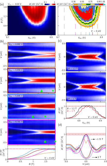
We next fix to a slightly different value and explore the zero-bias map in (, ) space, see Figure 2a. Besides the ‘red island’ as a ‘zone’, we use several discrete colors to label other ranges which are ‘boundary-like’. Fig. 2b shows four scans, see the corresponding colored dashed lines in Fig. 2a. The first scan is outside the ‘red island’ and resolves no ZBPs. Other scans pass through the ‘red island’ and resolve ZBPs near with different ranges. The green triangles and stars mark the on-set and ending values for ZBPs. The ZBP region defined by the green dashed lines in Fig. 2a roughly matches the ‘red island’ and can serve as a -ZBP phase diagram. Note that not every line cut passing through the ‘red island’ can resolve a plateau feature. For example, the blue line in Fig. 2b is more ‘peaked-like’ near .
Fig. 2c shows scans of the ZBP at 1.2 T and 1 T, corresponding to the middle and edge of the ‘red island’, respectively. The zero-bias line cuts illustrate the evolution from ‘peak-like’ (red) to ‘plateau-like’ (black). Fig. 2d shows the line cuts from the four panels in Fig. 2b at = 0 T (dashed lines) and 1.73 T. At zero field, the subgap peaks have similar energies. At high field (1.73 T), some curves resolve ZBPs near while others resolve split peaks, reflecting the phase diagram boundaries. For ‘Waterfall’ plots and additional scans see Figs. S3 and S4.
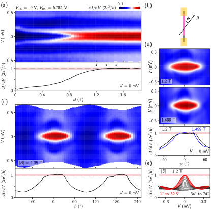
The next experimental knob is direction. rotation in Al-based systems was limited before due to orbital effects: the Al bulk gap is easily suppressed at low ( 0.3 T) during rotation [10]. Here, the ultra-thin diameter significantly suppresses the orbital effect and the gap can survive at high even if misaligned (see Fig. S2). This advantage enables a rotation for ZBP [38].
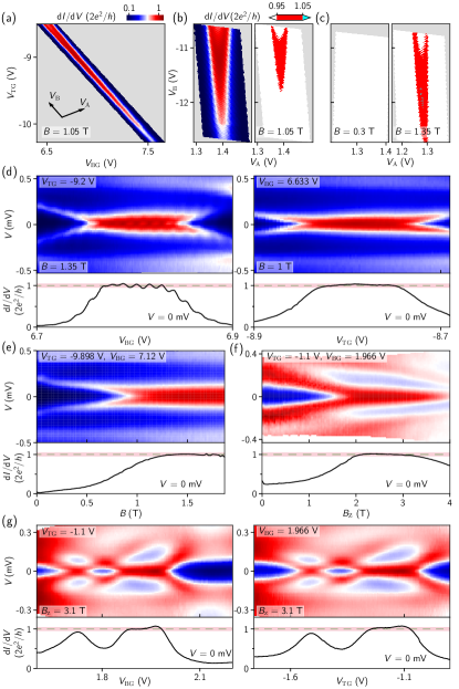
Figure 3a starts with a scan (aligned with the nanowire) of a ZBP near (note the minor charge jump at 1.7 T). The amplitude is then fixed at three values, see the arrows. Its direction, defined by the angle (Fig. 3b), is rotated. is in-plane during rotation (parallel to the substrate). Fig. 3c shows the angle dependence at 1.35 T. The ZBP remains close to over an angle range of 50∘. Outside this range, the ZBP height quickly decreases away from , accompanied by a gap closing. Finally, the ZBP vanishes at larger angles. For 170∘, the zero-bias conductance drops slightly below 0.95 due to a small peak-splitting which is separated by a minor charge jump. Fig. 3d shows the angle dependence at two other s, with line cuts shown in Fig. 3e. For more rotation scans, see Fig. S5.
For the last experimental check, we fix (aligned with the nanowire) at 1.05 T, and measure the zero-bias map in (, ) space, see Figure 4a. Due to the cross talks between the two gates, every gate can tune both the tunnel transmission in the barrier region and the electro-chemical potential in the proximitized wire. Therefore, the range is adjusted simultaneously for different settings to trace the same feature. To save space from the ‘no-data’ region (grey), we define new gate voltage axes: cos sin; sin cos. = 30∘. Fig. 4b re-plots Fig. 4a in (, ) axes. Together with Fig. 4c, the three-color plots show the gradual evolution of the ‘red island’: its area increases from none at low to a sizable zone at high . For a complete evolution, see Fig. S6. Figs. 4d and 4e show three additional examples of ZBP scans within this parameter region.
So far, all the ZBPs (from Fig. 1d to Fig. 4e) are within one single region (region I) in the multi-dimensional parameter space (, , ), see Fig. S7 for additional scans in this region. The measurement in region I lasts for three weeks with several charge jumps in between. We note the effects of jumps and hysteresis mainly shift the gate voltages, maximally by 300 mV. The main plateau features still remain after the shift with minor variations.
Fig. 4f and 4g demonstrate another plateau region (region II) at a very different (, , ) setting from region I. To access higher s, we apply along the fridge z axis (). The small misalignment (8∘) between and the nanowire should not bring a big difference based on the rotation experiment in Fig. 3. In Fig. 4f, the zero-bias conductance can stick close to from 2 T to 3.28 T, a -range larger than 1.2 Tesla (with a tolerance of 5). Outside this range, the ZBP height drops continuously from with a faster decreasing rate, possibly due to the combined effects of gap closing and softening for larger than 3 T. The fridge base for Fig. 4f is slightly higher (can reach 30 mK) which may also play a role. Even within the plateau region, there is still a decreasing trend with a much smaller slope, possibly due to those mechanisms above.
The overall conductance (barrier transmission) in region II is higher than that in region I, leading to a larger subgap conductance. Fig. 4g illustrates the interaction between the zero-energy state and a quantum dot level, possibly formed near the barrier. Tuning the dot level towards zero energy causes the splitting of the ZBP, similar to the behavior of partially separated MZMs [39, 40]. We translate the plateau width in to an energy scale of 260 eV based on our extracted lever arm. For additional scans of region II, see Fig. S8. Though the plateau regions (I and II) in gate voltage space is small, only 50 - 100 mV. Its corresponding energy scale, 260 - 300 eV, is much larger than the thermal energy.
We note that this work addresses the question ‘whether ZBP-plateaus near exist by sweeping all relevant experimental parameters’. It, however, cannot answer the question ‘whether similar plateaus (for sweeping all parameters) also exist at non-quantized values’. That would require exhausting the entire parameter space in more devices. Based on the collected data so far, we have not observed similar plateaus at other values yet. See Fig. S9 for additional ZBP data due to quantum dots and disorder in regions beyond I and II. Occasionally, we could find ‘plateau-like’ features above for one-parameter sweeping (but not all). We notice that for multiple subband occupation, even MZM could lead to some ‘plateau-like’ features above in the open barrier regime with slight disorder [8]. Finally, we compare some scans in Fig. S10 to illustrate the interplay between the barrier transmission and the ZBP height.
To summarize, we have observed ZBPs near which form a plateau mostly within tolerance by sweeping gate voltages and magnetic field. Our result is qualitatively consistent with the (multi-subband) MZM as well as quasi-MZM theories: the first is topological while the second is trivial and caused by non-uniform potential or disorder. The quasi-MZM scenario is probably more likely. This work is from a single device whose quality is an improvement compared to our previous one [14] but still not in the ballistic regime yet due to the obvious presence of quantum dots and disorder. Besides the ‘end-to-end’ correlation experiment to reveal gap-closing-reopening [41, 42, 43], future devices on ‘single-terminal’ experiments could aim at 1) looking for zero-bias peak-to-dip transition near with better tolerance [16, 19, 14]; 2) using a dissipative probe to reveal quantized ZBPs and suppress others [44, 45, 46, 47, 48]; 3) exploring potentially better material systems [49, 50].
I Acknowledgment
We thank Leo Kouwenhoven for comments. Raw data is available at https://doi.org/10.5281/zenodo.6546974. This work is supported by Tsinghua University Initiative Scientific Research Program, Alibaba Innovative Research Program, National Natural Science Foundation of China (Grant Nos. 12104053, 92065106, 92065206, 61974138, 12004040, 11974198). D.P. also acknowledges the support from Youth Innovation Promotion Association, Chinese Academy of Sciences (Nos. 2017156 and Y2021043).
References
- Read and Green [2000] N. Read and D. Green, Paired states of fermions in two dimensions with breaking of parity and time-reversal symmetries and the fractional quantum hall effect, Phys. Rev. B 61, 10267 (2000).
- Kitaev [2001] A. Y. Kitaev, Unpaired majorana fermions in quantum wires, Physics-Uspekhi 44, 131 (2001).
- Lutchyn et al. [2010] R. M. Lutchyn, J. D. Sau, and S. Das Sarma, Majorana fermions and a topological phase transition in semiconductor-superconductor heterostructures, Phys. Rev. Lett. 105, 077001 (2010).
- Oreg et al. [2010] Y. Oreg, G. Refael, and F. von Oppen, Helical liquids and majorana bound states in quantum wires, Phys. Rev. Lett. 105, 177002 (2010).
- Sengupta et al. [2001] K. Sengupta, I. Žutić, H.-J. Kwon, V. M. Yakovenko, and S. D. Sarma, Midgap edge states and pairing symmetry of quasi-one-dimensional organic superconductors, Physical Review B 63, 144531 (2001).
- Law et al. [2009] K. T. Law, P. A. Lee, and T. K. Ng, Majorana fermion induced resonant andreev reflection, Physical Review Letters 103, 237001 (2009).
- Flensberg [2010] K. Flensberg, Tunneling characteristics of a chain of majorana bound states, Physical Review B 82, 180516 (2010).
- Wimmer et al. [2011] M. Wimmer, A. Akhmerov, J. Dahlhaus, and C. Beenakker, Quantum point contact as a probe of a topological superconductor, New Journal of Physics 13, 053016 (2011).
- Mourik et al. [2012] V. Mourik, K. Zuo, S. M. Frolov, S. Plissard, E. P. Bakkers, and L. P. Kouwenhoven, Signatures of majorana fermions in hybrid superconductor-semiconductor nanowire devices, Science 336, 1003 (2012).
- Deng et al. [2016] M. Deng, S. Vaitiekėnas, E. B. Hansen, J. Danon, M. Leijnse, K. Flensberg, J. Nygård, P. Krogstrup, and C. M. Marcus, Majorana bound state in a coupled quantum-dot hybrid-nanowire system, Science 354, 1557 (2016).
- Nichele et al. [2017] F. Nichele, A. C. Drachmann, A. M. Whiticar, E. C. O’Farrell, H. J. Suominen, A. Fornieri, T. Wang, G. C. Gardner, C. Thomas, A. T. Hatke, et al., Scaling of majorana zero-bias conductance peaks, Physical review letters 119, 136803 (2017).
- Gül et al. [2018] Ö. Gül, H. Zhang, J. D. Bommer, M. W. de Moor, D. Car, S. R. Plissard, E. P. Bakkers, A. Geresdi, K. Watanabe, T. Taniguchi, et al., Ballistic majorana nanowire devices, Nature Nanotechnology 13, 192 (2018).
- Zhang et al. [2021] H. Zhang, M. W. de Moor, J. D. Bommer, D. Xu, G. Wang, N. van Loo, C.-X. Liu, S. Gazibegovic, J. A. Logan, D. Car, R. L. M. Op het Veld, P. J. van Veldhoven, S. Koellinga, M. A. Verheijen, M. Pendharkar, D. J. Pennachio, B. Shojaei, J. S. Lee, C. J. Palmstrøm, E. P. Bakkers, S. Das Sarma, and L. P. Kouwenhoven, Large zero-bias peaks in insb-al hybrid semiconductor-superconductor nanowire devices, arXiv: 2101.11456 (2021).
- Song et al. [2022] H. Song, Z. Zhang, D. Pan, D. Liu, Z. Wang, Z. Cao, L. Liu, L. Wen, D. Liao, R. Zhuo, D. E. Liu, R. Shang, J. Zhao, and H. Zhang, Large zero bias peaks and dips in a four-terminal thin inas-al nanowire device, Phys. Rev. Research 4, 033235 (2022).
- Prada et al. [2020] E. Prada, P. San-Jose, M. W. de Moor, A. Geresdi, E. J. Lee, J. Klinovaja, D. Loss, J. Nygård, R. Aguado, and L. P. Kouwenhoven, From andreev to majorana bound states in hybrid superconductor–semiconductor nanowires, Nature Reviews Physics 2, 575 (2020).
- Zhang et al. [2019] H. Zhang, D. E. Liu, M. Wimmer, and L. P. Kouwenhoven, Next steps of quantum transport in majorana nanowire devices, Nature Communications 10, 5128 (2019).
- Kells et al. [2012] G. Kells, D. Meidan, and P. Brouwer, Near-zero-energy end states in topologically trivial spin-orbit coupled superconducting nanowires with a smooth confinement, Physical Review B 86, 100503 (2012).
- Prada et al. [2012] E. Prada, P. San-Jose, and R. Aguado, Transport spectroscopy of ns nanowire junctions with majorana fermions, Physical Review B 86, 180503 (2012).
- Vuik et al. [2019] A. Vuik, B. Nijholt, A. Akhmerov, and M. Wimmer, Reproducing topological properties with quasi-majorana states, SciPost Physics 7, 061 (2019).
- Moore et al. [2018] C. Moore, C. Zeng, T. D. Stanescu, and S. Tewari, Quantized zero-bias conductance plateau in semiconductor-superconductor heterostructures without topological majorana zero modes, Physical Review B 98, 155314 (2018).
- Peñaranda et al. [2018] F. Peñaranda, R. Aguado, P. San-Jose, and E. Prada, Quantifying wave-function overlaps in inhomogeneous majorana nanowires, Phys. Rev. B 98, 235406 (2018).
- Cao et al. [2019] Z. Cao, H. Zhang, H.-F. Lü, W.-X. He, H.-Z. Lu, and X. C. Xie, Decays of majorana or andreev oscillations induced by steplike spin-orbit coupling, Phys. Rev. Lett. 122, 147701 (2019).
- Avila et al. [2019] J. Avila, F. Peñaranda, E. Prada, P. San-Jose, and R. Aguado, Non-hermitian topology as a unifying framework for the andreev versus majorana states controversy, Communications Physics 2 (2019).
- Pan and Das Sarma [2020] H. Pan and S. Das Sarma, Physical mechanisms for zero-bias conductance peaks in majorana nanowires, Phys. Rev. Research 2, 013377 (2020).
- Das Sarma and Pan [2021] S. Das Sarma and H. Pan, Disorder-induced zero-bias peaks in majorana nanowires, Phys. Rev. B 103, 195158 (2021).
- Zeng et al. [2022] C. Zeng, G. Sharma, S. Tewari, and T. Stanescu, Partially separated majorana modes in a disordered medium, Phys. Rev. B 105, 205122 (2022).
- Lai et al. [2022] Y.-H. Lai, S. Das Sarma, and J. D. Sau, Quality factor for zero-bias conductance peaks in majorana nanowire, Phys. Rev. B 106, 094504 (2022).
- Pan and Das Sarma [2022] H. Pan and S. Das Sarma, On-demand large conductance in trivial zero-bias tunneling peaks in majorana nanowires, Phys. Rev. B 105, 115432 (2022).
- Pan et al. [2022a] H. Pan, J. D. Sau, and S. Das Sarma, Random matrix theory for the robustness, quantization, and end-to-end correlation of zero-bias conductance peaks in a class d ensemble, Phys. Rev. B 106, 115413 (2022a).
- Pan et al. [2022b] D. Pan, H. Song, S. Zhang, L. Liu, L. Wen, D. Liao, R. Zhuo, Z. Wang, Z. Zhang, S. Yang, J. Ying, W. Miao, R. Shang, H. Zhang, and J. Zhao, In situ epitaxy of pure phase ultra-thin inas-al nanowires for quantum devices, Chinese Physics Letters 39, 058101 (2022b).
- Pientka et al. [2012] F. Pientka, G. Kells, A. Romito, P. W. Brouwer, and F. Von Oppen, Enhanced zero-bias majorana peak in the differential tunneling conductance of disordered multisubband quantum-wire/superconductor junctions, Physical review letters 109, 227006 (2012).
- Rainis et al. [2013] D. Rainis, L. Trifunovic, J. Klinovaja, and D. Loss, Towards a realistic transport modeling in a superconducting nanowire with majorana fermions, Physical Review B 87, 024515 (2013).
- Liu et al. [2017a] C.-X. Liu, J. D. Sau, and S. Das Sarma, Role of dissipation in realistic majorana nanowires, Phys. Rev. B 95, 054502 (2017a).
- Liu et al. [2017b] C.-X. Liu, F. Setiawan, J. D. Sau, and S. Das Sarma, Phenomenology of the soft gap, zero-bias peak, and zero-mode splitting in ideal majorana nanowires, Phys. Rev. B 96, 054520 (2017b).
- Takei et al. [2013] S. Takei, B. M. Fregoso, H.-Y. Hui, A. M. Lobos, and S. D. Sarma, Soft superconducting gap in semiconductor majorana nanowires, Physical review letters 110, 186803 (2013).
- Chang et al. [2015] W. Chang, S. Albrecht, T. Jespersen, F. Kuemmeth, P. Krogstrup, J. Nygård, and C. M. Marcus, Hard gap in epitaxial semiconductor–superconductor nanowires, Nature nanotechnology 10, 232 (2015).
- Zhang et al. [2017] H. Zhang, Ö. Gül, S. Conesa-Boj, M. P. Nowak, M. Wimmer, K. Zuo, V. Mourik, F. K. De Vries, J. Van Veen, M. W. De Moor, et al., Ballistic superconductivity in semiconductor nanowires, Nature Communications 8, 16025 (2017).
- Bommer et al. [2019] J. D. Bommer, H. Zhang, Ö. Gül, B. Nijholt, M. Wimmer, F. N. Rybakov, J. Garaud, D. Rodic, E. Babaev, M. Troyer, et al., Spin-orbit protection of induced superconductivity in majorana nanowires, Physical Review Letters 122, 187702 (2019).
- Prada et al. [2017] E. Prada, R. Aguado, and P. San-Jose, Measuring majorana nonlocality and spin structure with a quantum dot, Physical Review B 96, 085418 (2017).
- Clarke [2017] D. J. Clarke, Experimentally accessible topological quality factor for wires with zero energy modes, Physical Review B 96, 201109 (2017).
- Rosdahl et al. [2018] T. O. Rosdahl, A. Vuik, M. Kjaergaard, and A. R. Akhmerov, Andreev rectifier: A nonlocal conductance signature of topological phase transitions, Phys. Rev. B 97, 045421 (2018).
- Pan et al. [2021] H. Pan, J. D. Sau, and S. Das Sarma, Three-terminal nonlocal conductance in majorana nanowires: Distinguishing topological and trivial in realistic systems with disorder and inhomogeneous potential, Phys. Rev. B 103, 014513 (2021).
- Pikulin et al. [2021] D. Pikulin, B. van Heck, T. Karzig, E. A. Martinez, B. Nijholt, T. Laeven, G. W. Winkler, J. Watson, S. Heedt, M. Temurhan, V. Svidenko, R. Lutchyn, M. Thomas, G. de Lange, L. Casparis, and D. C. Nayak, Protocol to identify a topological superconducting phase in a three-terminal device, arXiv: 2103.12217 (2021).
- Liu [2013] D. E. Liu, Proposed method for tunneling spectroscopy with ohmic dissipation using resistive electrodes: a possible majorana filter, Physical Review Letters 111, 207003 (2013).
- Liu et al. [2020] D. Liu, Z. Cao, H. Zhang, and D. E. Liu, Revealing the nonlocal coherent nature of majorana devices from dissipative teleportation, Physical Review B 101, 081406 (2020).
- Liu et al. [2022] D. Liu, G. Zhang, Z. Cao, H. Zhang, and D. E. Liu, Universal conductance scaling of andreev reflections using a dissipative probe, Phys. Rev. Lett. 128, 076802 (2022).
- Zhang et al. [2022] S. Zhang, Z. Wang, D. Pan, H. Li, S. Lu, Z. Li, G. Zhang, D. Liu, Z. Cao, L. Liu, L. Wen, D. Liao, R. Zhuo, R. Shang, D. E. Liu, J. Zhao, and H. Zhang, Suppressing andreev bound state zero bias peaks using a strongly dissipative lead, Phys. Rev. Lett. 128, 076803 (2022).
- Wang et al. [2022] Z. Wang, S. Zhang, D. Pan, G. Zhang, Z. Xia, Z. Li, D. Liu, Z. Cao, L. Liu, L. Wen, D. Liao, R. Zhuo, Y. Li, D. E. Liu, R. Shang, J. Zhao, and H. Zhang, Large andreev bound state zero bias peaks in a weakly dissipative environment, arXiv: 2202.09299 (2022).
- Cao et al. [2022] Z. Cao, D. E. Liu, W.-X. He, X. Liu, K. He, and H. Zhang, Numerical study of pbte-pb hybrid nanowires for engineering majorana zero modes, Phys. Rev. B 105, 085424 (2022).
- Jiang et al. [2022] Y. Jiang, S. Yang, L. Li, W. Song, W. Miao, B. Tong, Z. Geng, Y. Gao, R. Li, F. Chen, Q. Zhang, F. Meng, L. Gu, K. Zhu, Y. Zang, R. Shang, Z. Cao, X. Feng, Q.-K. Xue, D. E. Liu, H. Zhang, and K. He, Selective area epitaxy of pbte-pb hybrid nanowires on a lattice-matched substrate, Phys. Rev. Materials 6, 034205 (2022).
See pages 1 of SM_LS18388.pdf See pages 2 of SM_LS18388.pdf See pages 3 of SM_LS18388.pdf See pages 4 of SM_LS18388.pdf See pages 5 of SM_LS18388.pdf See pages 6 of SM_LS18388.pdf See pages 7 of SM_LS18388.pdf See pages 8 of SM_LS18388.pdf See pages 9 of SM_LS18388.pdf