Optically-triggered strain-driven Néel vector manipulation in a metallic antiferromagnet
Abstract
The absence of stray fields, their insensitivity to external magnetic fields, and ultrafast dynamics make antiferromagnets promising candidates for active elements in spintronic devices. Here, we demonstrate manipulation of the Néel vector in the metallic collinear antiferromagnet Mn2Au by combining strain and femtosecond laser excitation. Applying tensile strain along either of the two in-plane easy axes and locally exciting the sample by a train of femtosecond pulses, we align the Néel vector along the direction controlled by the applied strain. The dependence on the laser fluence and strain suggests the alignment is a result of optically-triggered depinning of 90o domain walls and their sliding in the direction of the free energy gradient, governed by the magneto-elastic coupling. The resulting, switchable, state is stable at room temperature and insensitive to magnetic fields. Such an approach may provide ways to realize robust high-density memory device with switching timescales in the picosecond range.
Antiferromagnets (AFM) have recently attracted major scientific interest due to their prospective applications in the field of spintronics.[1, 2, 3, 4] For information storage, they offer several advantages over ferromagnets, such as a potential for ultrafast switching, the lack of stray fields and, thus, the robustness against external fields. All these properties could enable high information density, with the direction of the staggered magnetization (Néel vector, L) as the information carrier. The lack of sensitivity to external magnetic fields, however, poses challenges in terms of writing [5, 6, 7] and read-out [8, 7, 9, 10, 11] schemes. Exploring the ways to rapidly and reliably manipulate the Néel vector direction is at the heart of the current AFM spintronics research.[1, 2, 3, 4] Especially the metallic collinear antiferromagnets CuMnAs and Mn2Au, which enable current-induced bulk (Néel) spin-orbit torques,[12] have been in the focus of recent research. Several approaches for switching the direction of the Néel vector have been suggested, which include aligning the Néel vector by high magnetic fields,[13, 14] application of strain,[15, 16] and, most prominently, using current-driven Néel spin-orbit torques.[5, 6, 7] In terms of the read-out, in addition to X-ray magnetic linear dichroism,[13, 16, 17] electrical read-out via the anisotropic magnetoresistance (AMR)[5, 7] and optical magnetic linear dichroism (OMLD)[18, 10] have been realized. In spite the achieved progress, an ultrafast approach for locally changing the Néel vector orientation is needed to fully exploit the potential of AFMs in spintronics.
In this work, we demonstrate a novel approach to manipulate the Néel vector in a collinear metallic antiferromagnet Mn2Au by combining applied strain with femtosecond laser excitation. Exciting the strained Mn2Au film by a train of femtosecond near-infrared pulses, we align the Néel vector in the direction perpendicular to the applied tensile strain. Imaging the resulting magnetic domain structure by photoemission electron microscopy using X-ray magnetic linear dichroism to obtain magnetic contrast (XMLD-PEEM), we demonstrate the existence of a threshold fluence required for Néel vector alignment, which depends on the strain. Analyzing the magnetic domain structures before and after optical excitation, we attribute the observed optically activated Néel vector alignment in Mn2Au to depinning, motion and annihilation of the 90o domain walls. Based on the threshold fluence values and their dependence on strain, we suggest the depinning is activated by laser induced transient heating. The demonstrated method of local optical manipulation of the Néel vector can be applied to a range of collinear AFMs with low magneto-crystalline anisotropies, enabling ultrafast writing of magnetically stored information. In combination with fast optical readout schemes,[18, 10] this approach provides means for studying switching and domain wall dynamics on an ultrafast timescale.
Laser writing under tensile strain
The metallic collinear AFM Mn2Au has a body-centered tetragonal crystal structure. It is an easy plane AFM, with a strong out-of-plane [001] hard axis and a weak 4-fold in-plane magnetic anisotropy. The Mn spin orientations in adjacent planes are anti-parallel, with L pointing along one of the easy directions.[19, 20] The -axis epitaxial 45 nm thin Mn2Au films are grown on -cut (102) Al2O3 substrates, with a 13 nm Ta (001) buffer layer for improving epitaxial growth.[20] The directions of Mn2Au are parallel to the substrate edges, which are along the and directions of the -cut Al2O3 substrate (index stands for the substrate). We note, that recent optical study on similar films revealed a weak in-plane optical linear dichroism in the as-grown films, which was attributed to a weak, growth-induced, strain.[10] To take this underlying asymmetry into account, we label the two easy axes such that and .
The experimental approach to manipulate the Néel vector by combining tensile strain and femtosecond laser pulse excitation is sketched in Fig. 1 a,b (see Methods for details). Fifteen areas on the film are marked by a set of 30 nm thick Cr/Au markers fabricated on the top of the film using electron beam lithography. The areas are irradiated by a train of 60 fs laser pulses at 800 nm with excitation fluence in different marked areas varied between and mJ/cm2. The irradiated areas are 60-70 m in diameter, as indicated by the colored circles in Fig. 1b. Five areas are irradiated with the tensile strain along the direction, five areas with the tensile strain along the direction and five areas without applying external strain. The value of the tensile strain is , as measured by a Si strain gauge attached to the substrate.[15]
After laser irradiation under strain, we image the domain structure within all illuminated areas of the film using XMLD-PEEM.[21] For reference, we also recorded a number of images of non-illuminated areas across the sample. To quantitatively analyze the magnetic domain structure, we binarize the magnetic contrast images using an Otsu-threshold method[22] and calculate the area fractions of the two types of magnetic domains. The same procedure is applied to every image.
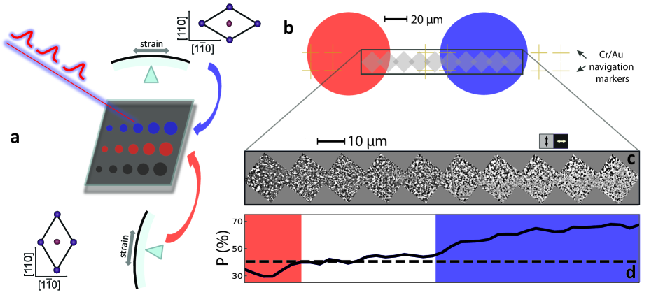
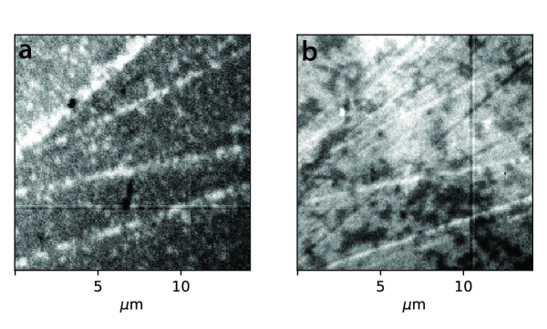
Figure 1c presents a sequence of successive XMLD-PEEM images acquired along the line connecting two adjacent marked areas, irradiated with fluence mJ/cm2 while the tensile strain was applied along the two orthogonal easy directions. The resulting deformations of the crystal lattice are schematically illustrated in Fig. 1a. On the left side, where the tensile strain was applied along the [110] direction, the domain structure exhibits preferentially domains with (dark), while on the right side, where the tensile strain was applied along the [10] direction, the majority of domains are with (bright).[15, 13, 10, 11] Between the two laser-irradiated areas, the domain structure is the same as in reference areas far away from the irradiated areas.
We quantify the state of magnetic alignment by , the area fraction of domains with the Néel vector parallel to the [110] direction. Figure 1d presents the variation of along the line connecting the two areas irradiated under orthogonal applied tensile strain. It follows that, under laser irradiation, the Néel vector aligns perpendicular to the direction of the applied tensile strain. Between the two irradiated areas we observe an uneven fraction of dark and bright domains with ; the same value of is found across the non-irradiated (as-grown) areas of the sample.
The dependence of light-induced Néel vector alignment on excitation fluence
To gain insight into the origin of the light-induced Néel vector switching, we analyze the fluence dependence of in the range of fluences between 3.5 and 10.6 mJ/cm2.
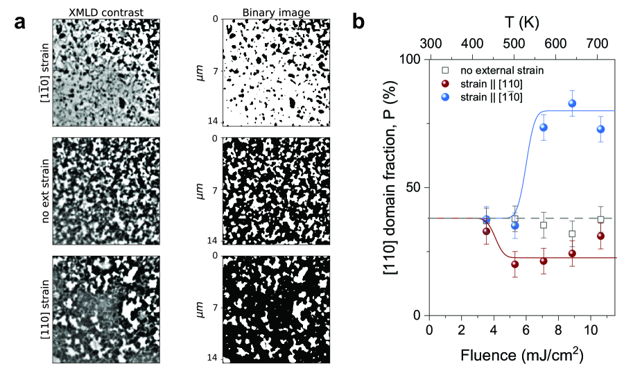
Figure 2 presents the dependence of the degree of alignment on the irradiation fluence, , for all three strain configurations. Figure 2a depicts the magnetic contrast images (left column) for sample areas irradiated under different external strain directions. From the corresponding binary images (right column) we obtain across m2 imaged areas.
Figure 2b displays for different external strain configurations. At mJ/cm2 we obtain independent on the applied strain, matching the value recorded on non-irradiated areas. The variation of at mJ/cm2 is similar to variation of in reference, non-irradiated, areas across the film and is governed by sample inhomogeneities. This variation can be considered as a measure of the experimental uncertainty of the extracted (error bars in Fig. 2b).
The value obtained for the as-grown film implies a partial Néel vector alignment. This observation is consistent with earlier imaging studies,[11, 10] and may be a result of the growth-induced strain.[10] Indeed, as discussed earlier,[23, 10] the -axis of Mn2Au films grown on a -cut Al2O3 substrate is tilted by 2-3o towards the direction.[10] While no underlying strain could be resolved in the diffraction experiments,[10] the tilted growth and the corresponding breaking of the four-fold symmetry may indicate a weak growth-induced strain being responsible for a larger volume fraction of domains with the Néel vector perpendicular to the direction of the -axis tilt.[10, 11]
Fig. 2b shows, that for both directions of the applied tensile strain there exists a threshold fluence, above which a Néel vector aligned state is realized. Here, the maximum degree of alignment, with either or , is comparable to the values obtained in Mn2Au films, where the Néel vector has been aligned in 60 T pulsed magnetic fields.[15, 13, 10] The threshold fluence appears to be different for the two orthogonal directions of the applied strain. For the case of tensile strain applied along the direction, the switched state is observed already at 5.3 mJ/cm2. On the other hand, for tensile strain applied along the Néel vector alignment is realized at mJ/cm2. Such a difference can be linked to the existing, growth-induced, strain in the as-grown film, which needs to be added to or subtracted from the external applied strain. Our results indicate, that the growth-induced strain could either be tensile, along the direction (the direction parallel to the tilt of the -axis and ), or compressive, along the direction (the direction parallel to and perpendicular to the direction of the -axis tilt).
Finally, when irradiating the sample in the absence of external strain, did not change within the range of excitation fluences used here.
Proposed mechanism of light-induced Néel vector alignment in Mn2Au
In experiments, where switching of the Néel vector in Mn2Au was realized by applying microsecond/millisecond current pulses, the reported current-induced sample heating was significant.[7, 24, 23] E.g., in Ref.7, a temperature increase near the switching threshold was estimated to be 300 K. Discussing current-driven switching in granular Mn2Au thin films, Meinert et al. proposed a phenomenological model of Néel spin-orbit torque (NSOT) - driven domain switching, assisted by sample heating.[24] There, the switching was considered to be a coherent process, i.e., individual domains (the grain size with nm lateral dimension) were considered to switch under the NSOT. Such a switching process, however, requires overcoming an energy barrier ,[24] where is the density of the in-plane bi-axial magneto-crystalline anisotropy energy and is the domain volume. Considering a thermally activated process, with the NSOT-driven switching rate , a qualitative agreement between their experimental results and the Monte Carlo simulations was obtained, assuming an attempt rate given by the characteristic frequency of antiferromagnets (1012 s-1) and eV.[24] With eV per formula unit,[11] such values of are expected for domains with length-scales of nm, as reported for Mn2Au films grown on ZrN-buffered MgO by Meinert et al.[24] However, considering the domains in our samples have a typical lateral size of 1 m, the corresponding would be in the range of 103 eV. Thus, such a coherent switching of individual domains is unlikely in our epitaxial films.
We propose the light-driven alignment of Néel vector in strained Mn2Au films to be a result of an activated domain wall motion. We first estimate the magneto-elastic coupling constant , which results in a difference in the free energy densities in orthogonally aligned magnetic domains. To this end, we performed DFT calculations of in Mn2Au (see Supplementary Information). We obtain meV per formula unit, which corresponds to a reduction in the free energy density for domains with Néel vector perpendicular to the direction of the applied tensile strain by eV per formula unit for the applied strain . This value is comparable to the in-plane magneto-crystalline anisotropy, eV per formula unit,[11] thus sufficient for Néel vector alignment. Indeed, an earlier XMLD spectroscopy study on similar films did demonstrate partial Néel vector alignment under similar values of the applied external strain.[15] However, after the applied strain was released, the original state was recovered, with no permanent Néel vector alignment.[15] In the absence of pinning of domain walls (DWs) the applied strain should force the motion of 90o DWs (DWs between domains with orthogonal L) in the direction of the free energy gradient, resulting in only two types of domains with anti-parallel L, separated by the 180o DWs. While it is pinning of the 90o DWs that prevents a stable Néel vector-aligned state to be realized using mechanical strain alone,[15] it is likely the laser-induced depinning of DWs that is governing the strain-driven laser-assisted Néel vector-alignment.
Assuming laser-assisted depinning of DWs being the mechanism of the Néel vector alignment, we need to consider the effect of photoexcitation with a train of femtosecond optical pulses. We first note that the continuous (average) laser heating is estimated to be K at the highest excitation densities used (see Supplementary Information) and can be neglected. Next, we estimate the induced changes in charge, spin and lattice subsystems following excitation with an ultrafast optical pulse. For simplicity, we consider the two-temperature model, that qualitatively accounts for the evolution of the electronic and lattice temperatures in metals on the (sub-)picosecond timescales.[25] Here, the electron-electron scattering results in carrier thermalization on the sub-picosecond timescale. The estimated electron temperatures for the two threshold fluences are 4600 K and 5400 K (see Supplementary Information), substantially exceeding the Néel temperature of Mn2Au ( K [19]). This is followed by thermalization with the lattice on a timescale of a few picoseconds and a subsequent heat diffusion into the substrate on a characteristic timescale of hundred picoseconds (see Supplementary Information). The calculated peak temperatures of the coupled electron-spin-lattice system, determined by the absorbed energy density and the total specific heat, are shown on the top axis of Fig. 2b. The temperature values are comparable to those reported in the current-driven switching experiments.[7, 24, 23]
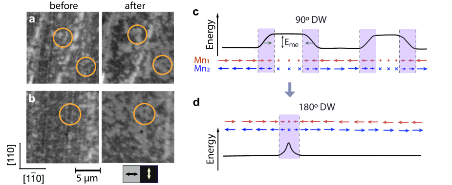
To shed light on the proposed mechanism, we performed complementary optical excitation experiments on a Mn2Au films, Néel vector aligned in a 60 T magnetic field. In this case laser-irradiation was performed in the absence of an external strain, and XMLD-PEEM images for several marked areas were recorded before and after laser irradiation. Considering the existence of the growth-induced strain, one may expect a similar process of light-assisted DW depinning, resulting in a state with , as in as-grown films. To have a maximum contrast between before and after irradiation we investigated Mn2Au film, magnetically aligned along the direction in a 60 T magnetic field, with .
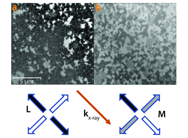
Analyzing XMLD-PEEM images before and after laser irradiation reveals a switching threshold of mJ/cm2. Figure 3 a,b presents the XMLD-PEEM images recorded before and after irradiation for near-threshold excitation at mJ/cm2. XMLD-PEEM images of the B-field aligned sample before irradiation (left panels) show predominantly domains with (). After irradiation with mJ/cm2 (right panels), the majority of domains have , with . Surprisingly, for mJ/cm2 the value of is reached (see Supplementary Figure 2), similar to the case of the sample irradiated with mJ/cm2 under the applied external strain along the direction. The observed light-induced Néel vector alignment in the absence of applied strain lends further support to the existence of a weak growth-induced strain in films grown on -cut Al2O3 substrates. Its presence is likely responsible for the observed light-induced switching of L in the absence of applied strain as well as for the partial alignment of the Néel vector in as-grown films. Furthermore, the results imply the as-grown state with is actually a metastable state, the state with being the state with the lowest free energy.
To unambiguously show that it is the photoexcitation-assisted depinning of the DWs that governs the Néel vector alignment in Mn2Au under strain, an in situ time-dependent XMLD-PEEM study would be required. There are, however, several observations that, indirectly, provide support to the proposed mechanism.
The XMLD-PEEM images of a B-field aligned sample before and after laser irradiation at the threshold fluence (Fig. 3 a,b) are consistent with the laser-induced domain growth. This can be inferred from areas, highlighted by orange circles, displaying growth of the minority domains following photoexcitation of -aligned sample.
Secondly, our proposed mechanism suggests that depinning of the 90o DWs results in the DW motion in the direction of the free energy gradient (Fig. 3 c), and subsequent DW annihilation or formation of stable 180o DWs (Fig. 3 d). The resulting state should ideally consist of domains with antiparallel Néel vectors, separated by the 180o DWs. Indeed, in both current-driven[23] and strain-driven switching experiments worm-like structures are observed in XMLD-PEEM images, attributed to 180o DWs. A clear support to this assignment is provided by Supplementary Fig. 3, where the domain structure of the optically switched area is imaged by both XMLD and X-ray magnetic circular dichroism (XMCD) PEEM (see Supplementary Information for details).
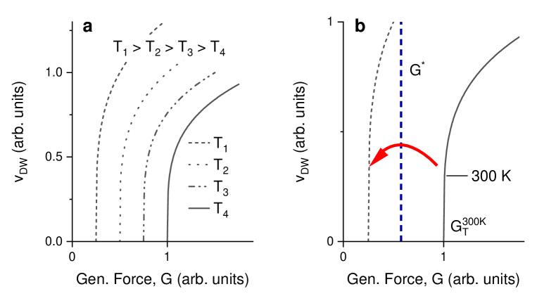
Finally, the observation of the switching threshold and its dependence on strain further supports the proposed mechanism. The fact that the magnetically aligned state is clearly observed only for fluences above the threshold fluence (or the related threshold temperature) suggests a thermally activated depinning transition.[26] At a fixed temperature, the depinning transition from a pinned DW is realized by increasing the driving force, (in our case given by the gradient in the magneto-elastic energy, which is proportional to strain), above its threshold value, , resulting in DW sliding (see Supplementary Fig. 4a). It has been demonstrated both theoretically[27, 28, 26] and experimentally[29, 30] that decreases with increasing temperature. At high temperatures with the exponent depending on the details of the pinning centers and interactions.[27, 28, 26] Let us assume that the application of a tensile strain results in an effective force , which is lower than at the base temperature. This is supported by the lack of permanent magnetic alignment when using only tensile-strain.[15] Photoexcitation results in an increase in local sample temperature, causing a transient reduction in to below and, thus, launching a sliding DW motion (see Supplementary Fig. 4). This scenario naturally accounts for the variation in threshold fluence on the applied tensile strain. As and, thus, differs in the two strain configurations (the growth-induced strain has to be added/subtracted from the applied strain), the observed difference in threshold fluences (temperatures) can be attributed to the presence of the growth-induced strain. In fact, the observation of even higher threshold fluence for switching the B-field aligned film in the absence of external strain further supports this scenario.
Conclusions
We present a new approach to locally manipulate the Néel vector alignment in the collinear metallic antiferromagnet Mn2Au by combining strain and excitation with femtosecond laser pulses. To achieve switching, we applied an external strain, which was large enough to induce an additional two-fold anisotropy, yet not strong enough to induce a depinning transition at room temperature. By irradiation of the sample with the train of femtosecond laser pulses we managed to locally align the Néel vector in two orthogonal orientations, with the direction controlled by the direction of the applied tensile strain, i.e., we realize stable "zero" and "one" states on the same film. This approach allows selective/local control of the Néel vector axis, with spatial resolution that could be further reduced to a sub-wavelength range by using near-field approaches.
The proposed mechanism of magnetic alignment via DW depinning may also be at play in the current-switching experiments in Mn2Au and CuMnAs.[5, 6, 7, 24, 23] While for current-switching of Mn2Au and CuMnAs the driving force is provided by the NSOT, thermal activation could be relevant.[7, 24] In both configurations, however, increasing the effective driving force , or decreasing of the DW depinning threshold, , may substantially reduce the required heating to reach domain-wall depinning regime. To this end, further optimization of the film growth, including using different substrate/buffer layer combinations, is required.
While we demonstrate the Néel vector alignment triggered by femtosecond laser pulses, and present evidence, suggesting the process is governed by the depinning of domain walls, the details of the underlying process, including timescales, remain to be investigated. To confirm the proposed scenario by recording the dynamics of the domain growth, an ultrafast laser amplifier with sufficient fluence should be coupled to the XMLD-PEEM end-station to enable in situ imaging following single laser-pulse excitation. With domains on the micrometer lengthscale and a substantial magnetic linear dichroism in the near-infrared[10] imaging the domain structure with femtosecond near-infrared pulses can also be realized. In this case, combining the optical pump-probe approach with fast modulation of strain (synchronized to the laser repetition rate) could present a way to study domain-wall dynamics on the picosecond timescale. This would be particularly interesting in systems like Mn2Au, where theoretical studies suggest that domain-wall velocities as high as 30 km/s could be achieved.[14]
Should such high DW velocities[14] indeed be realized, a characteristic timescale for optically-induced alignment of micrometer areas would be on the 10-100 ps range, which could enable optical switching with single pulses. Given the fact that the resulting state is stable at room temperature and insensitive to magnetic fields up to several tens of Tesla,[15, 13, 10] a combination of global strain modulation and local ultrafast manipulation of Néel vector may provide ways to realize robust high-density memory device with switching timescales in the picosecond range.
Methods
Mn2Au thin films
The -axis epitaxial Mn2Au thin films are grown on -cut (102) Al2O3 substrate, with the lateral size of 1010 mm2 and thickness of 530 m by the radio-frequency magnetron sputtering at 600 ∘C - see [20] for details. A 40 nm thick Mn2Au film was deposited on a 13 nm thick (001) Ta buffer layer. To protect the surface, a 2 nm Al layer was deposited on Mn2Au, forming an aluminum-oxide capping layer. Mn2Au grows epitaxially with [110] and [10] axes parallel to the substrate edges, which are along the and directions of the -cut Al2O3 substrate, respectively. The -axis of Mn2Au films grown on -cut Al2O3 are tilted by 2-3∘ towards the direction.
Laser irradiation under tensile strain
The experimental approach to manipulate the Néel vector by combination of tensile strain and laser pulse excitation is sketched in Fig. 1 a,b.
In the first step, a set of 30 nm thick Cr/Au markers is fabricated on the top of the film using electron beam lithography - see the schematic layout in Fig. 1b. These markers allow us to identify distinct areas of approximately m2 in the following steps. The sample is then mounted on a stress device, as used in Ref. 15. Bending the substrate results in tensile strain in the thin Mn2Au film along the [110] direction (see Fig. 1a). The resulting strain is approximately , as measured by a Si strain gauge attached to the substrate.[15] Then, several marked areas of the film are irradiated by a pulsed laser beam. We use 60 fs pulses at 800 nm and 250 kHz repetition rate. The excitation fluence used in different marked areas is varied between and mJ/cm2. The linearly polarized laser beam (the effect is found to be independent of the light polarization) is focused onto a spot with m in diameter (full-width at half maximum). Each marked area is irradiated for several seconds by scanning the beam around the center of the marked area, resulting in the size of the irradiated area of about m in diameter, as indicated by the colored areas in Fig. 1b.
In the next step, the sample is remounted on the strain device and a similar tensile strain is applied along the [10] direction and a different set of marked areas is irradiated (Fig. 1a). Finally, a series of marked areas is irradiated without the applied tensile strain. In total, five marked areas on the film are irradiated without applying external strain, five with the tensile strain along the direction and five with tensile strain along the direction.
A commercial 250 kHz Ti:Sapphire amplifier producing 60 fs laser pulses at = 800 nm (photon energy of 1.55 eV) was used to excite the strained thin films.
Imaging of Mn2Au films using XMLD-PEEM
The XMLD-PEEM experiments were performed at the SIM beamline of the Swiss Light Source. The sample was illuminated by linearly polarized X-rays with both s- and p- polarizations. The angle of incidence was 16∘. To achieve the best contrast, we utilized a slightly modified method than that described in Ref. 23. Namely, we acquired images with two orthogonal linear polarizations of the X-rays at each of the two photon energies (in this case 637.6 eV and 638.6 eV) around the absorption edge of Mn, corresponding to maximal XMLD contrast.[15] The resulting XMLD-PEEM images were obtained by pixelwise division of XMLD contrast maps recorded at 638.6 eV and 637.6 eV, where each XMLD was determined by the normalized difference of images acquired with the two orthogonal X-ray polarizations. The field of view used is 20 m.
References
- [1] MacDonald, A. H. & Tsoi, M. Antiferromagnetic metal spintronics. \JournalTitlePhil. Trans. R. Soc. A. 369, 3098–3114, DOI: 10.1098/rsta.2011.0014 (2011).
- [2] Jungwirth, T., Marti, X., Wadley, P. & Wunderlich, J. Antiferromagnetic spintronics. \JournalTitleNature Nanotech 11, 231–241, DOI: 10.1038/nnano.2016.18 (2016).
- [3] Baltz, V. et al. Antiferromagnetic spintronics. \JournalTitleRev. Mod. Phys. 90, 015005, DOI: 10.1103/RevModPhys.90.015005 (2018).
- [4] Němec, P., Fiebig, M., Kampfrath, T. & Kimel, A. V. Antiferromagnetic opto-spintronics. \JournalTitleNature Physics 14, 229–241, DOI: 10.1038/s41567-018-0051-x (2018).
- [5] Wadley, P. et al. Electrical switching of an antiferromagnet. \JournalTitleScience 351, 587–590, DOI: 10.1126/science.aab1031 (2016).
- [6] Olejník, K. et al. Terahertz electrical writing speed in an antiferromagnetic memory. \JournalTitleScience Advances 4, eaar3566, DOI: 10.1126/sciadv.aar3566 (2018).
- [7] Bodnar, S. Y. et al. Writing and reading antiferromagnetic Mn2Au by Néel spin-orbit torques and large anisotropic magnetoresistance. \JournalTitleNat. Commun. 9, 348, DOI: 10.1038/s41467-017-02780-x (2018).
- [8] Grzybowski, M. J. et al. Imaging current-induced switching of antiferromagnetic domains in CuMnAs. \JournalTitlePhys. Rev. Lett. 118, 057701, DOI: 10.1103/PhysRevLett.118.057701 (2017).
- [9] Schreiber, F. et al. Concurrent magneto-optical imaging and magneto-transport readout of electrical switching of insulating antiferromagnetic thin films. \JournalTitleApplied Physics Letters 117, 082401, DOI: 10.1063/5.0011852 (2020).
- [10] Grigorev, V. et al. Optical readout of the Néel vector in the metallic antiferromagnet Mn2Au. \JournalTitlePhys. Rev. Applied 16, 014037, DOI: 10.1103/PhysRevApplied.16.014037 (2021).
- [11] Bommanaboyena, S. P. et al. Readout of an antiferromagnetic spintronics system by strong exchange coupling of Mn2Au and Permalloy. \JournalTitleNature Communications 12, 1–7, DOI: 10.1038/s41467-021-26892-7 (2021).
- [12] Železnỳ, J. et al. Relativistic Néel-order fields induced by electrical current in antiferromagnets. \JournalTitlePhysical review letters 113, 157201, DOI: 10.1103/PhysRevLett.113.157201 (2014).
- [13] Sapozhnik, A. et al. Direct imaging of antiferromagnetic domains in Mn2Au manipulated by high magnetic fields. \JournalTitlePhysical Review B 97, 134429, DOI: 10.1103/PhysRevB.97.134429 (2018).
- [14] Gomonay, O., Kläui, M. & Sinova, J. Manipulating antiferromagnets with magnetic fields: Ratchet motion of multiple domain walls induced by asymmetric field pulses. \JournalTitleApplied Physics Letters 109, 142404, DOI: 10.1063/1.4964272 (2016).
- [15] Sapozhnik, A. A. et al. Manipulation of antiferromagnetic domain distribution in Mn2Au by ultrahigh magnetic fields and by strain. \JournalTitlephysica status solidi (RRL) - Rapid Research Letters 11, 1600438, DOI: https://doi.org/10.1002/pssr.201600438 (2017).
- [16] Chen, X. et al. Electric field control of Néel spin-orbit torque in an antiferromagnet. \JournalTitleNature Materials 18, 931–935, DOI: 10.1038/s41563-019-0424-2 (2019).
- [17] Wadley, P. et al. Current polarity-dependent manipulation of antiferromagnetic domains. \JournalTitleNature Nanotechnology 13, 362–365, DOI: 10.1038/s41565-018-0079-1 (2018).
- [18] Surỳnek, M. et al. Investigation of magnetic anisotropy and heat dissipation in thin films of compensated antiferromagnet CuMnAs by pump–probe experiment. \JournalTitleJournal of Applied Physics 127, 233904, DOI: 10.1063/5.0006185 (2020).
- [19] Barthem, V., Colin, C., Mayaffre, H., Julien, M.-H. & Givord, D. Revealing the properties of Mn2Au for antiferromagnetic spintronics. \JournalTitleNature Communications 4, 1–7, DOI: 10.1038/ncomms3892 (2013).
- [20] Bommanaboyena, S., Bergfeldt, T., Heller, R., Kläui, M. & Jourdan, M. High quality epitaxial Mn2Au (001) thin films grown by molecular beam epitaxy. \JournalTitleJournal of Applied Physics 127, 243901, DOI: 10.1063/5.0009566 (2020).
- [21] Le Guyader, L. et al. Studying nanomagnets and magnetic heterostructures with x-ray peem at the swiss light source. \JournalTitleJournal of Electron Spectroscopy and Related Phenomena 185, 371–380, DOI: 10.1016/j.elspec.2012.03.001 (2012).
- [22] Xu, X., Xu, S., Jin, L. & Song, E. Characteristic analysis of Otsu threshold and its applications. \JournalTitlePattern Recognition Letters 32, 956–961, DOI: 10.1016/j.patrec.2011.01.021 (2011).
- [23] Bodnar, S. Y. et al. Imaging of current induced Néel vector switching in antiferromagnetic Mn2Au. \JournalTitlePhys. Rev. B 99, 140409, DOI: 10.1103/PhysRevB.99.140409 (2019).
- [24] Meinert, M., Graulich, D. & Matalla-Wagner, T. Electrical switching of antiferromagnetic Mn2Au and the role of thermal activation. \JournalTitlePhys. Rev. Applied 9, 064040, DOI: 10.1103/PhysRevApplied.9.064040 (2018).
- [25] Obergfell, M. & Demsar, J. Tracking the time evolution of the electron distribution function in copper by femtosecond broadband optical spectroscopy. \JournalTitlePhys. Rev. Lett. 124, 037401, DOI: 10.1103/PhysRevLett.124.037401 (2020).
- [26] Brazovskii, S. & †, T. N. Pinning and sliding of driven elastic systems: from domain walls to charge density waves. \JournalTitleAdvances in Physics 53, 177–252, DOI: 10.1080/00018730410001684197 (2004).
- [27] Ioffe, L. B. & Vinokur, V. M. Dynamics of interfaces and dislocations in disordered media. \JournalTitleJournal of Physics C: Solid State Physics 20, 6149–6158, DOI: 10.1088/0022-3719/20/36/016 (1987).
- [28] Nattermann, T., Pokrovsky, V. & Vinokur, V. M. Hysteretic dynamics of domain walls at finite temperatures. \JournalTitlePhys. Rev. Lett. 87, 197005, DOI: 10.1103/PhysRevLett.87.197005 (2001).
- [29] Gorchon, J. et al. Pinning-dependent field-driven domain wall dynamics and thermal scaling in an ultrathin magnetic film. \JournalTitlePhys. Rev. Lett. 113, 027205, DOI: 10.1103/PhysRevLett.113.027205 (2014).
- [30] Diaz Pardo, R., Savero Torres, W., Kolton, A. B., Bustingorry, S. & Jeudy, V. Universal depinning transition of domain walls in ultrathin ferromagnets. \JournalTitlePhys. Rev. B 95, 184434, DOI: 10.1103/PhysRevB.95.184434 (2017).
- [31] Kresse, G. & Furthmüller, J. Efficient iterative schemes for ab initio total-energy calculations using a plane-wave basis set. \JournalTitlePhys. Rev. B 54, 11169–11186, DOI: 10.1103/PhysRevB.54.11169 (1996).
- [32] Perdew, J. P., Burke, K. & Ernzerhof, M. Generalized gradient approximation made simple. \JournalTitlePhys. Rev. Lett. 77, 3865–3868, DOI: 10.1103/PhysRevLett.77.3865 (1996).
- [33] Shick, A. B., Khmelevskyi, S., Mryasov, O. N., Wunderlich, J. & Jungwirth, T. Spin-orbit coupling induced anisotropy effects in bimetallic antiferromagnets: A route towards antiferromagnetic spintronics. \JournalTitlePhys. Rev. B 81, 212409, DOI: 10.1103/PhysRevB.81.212409 (2010).
- [34] Nieves, P. et al. Maelas: Magneto-elastic properties calculation via computational high-throughput approach. \JournalTitleComputer Physics Communications 264, 107964, DOI: 10.1016/j.cpc.2021.107964 (2021).
- [35] Carslaw, H. S. & Jaeger, J. C. Conduction of heat in solids (Clarendon press, 1992).
- [36] Mihailovic, D. & Demsar, J. Time-Resolved Optical Studies of Quasiparticle Dynamics in High-Temperature Superconductors: Experiments and Theory, chap. 16, 230–244 (American Chemical Society, 1999).
- [37] Burghartz, S. & Schulz, B. Thermophysical properties of sapphire, AlN and MgAl2O4 down to 70 K. \JournalTitleJournal of nuclear materials 212, 1065–1068 (1994).
Acknowledgments
This work was funded by the Deutsche Forschungsgemeinschaft (DFG, German Research Foundation) Grant No. TRR 173 - 268565370 (project A05, with contribution from A01) and TRR 288 - 422213477 (project B08) and received support from Horizon 2020 Framework Program of the European Commission under grant agreement No. 863155 (S-NEBULA). V.G. and M.F. acknowledge the financial support from the Graduate School of Excellence "Materials Science in Mainz" (DFG GSC 266 49741853). P.G. gratefully acknowledge support from the Agence Nationale de Recherche, via the MeMoPas project ANR-19-CE46-0006-1, as well as access to the HPC resources of IDRIS under the allocation A0090910965 attributed by GENCI. We acknowledge the Paul Scherrer Institute, Villigen, Switzerland for the beamtime allocation under proposal 20200977 at the SIM beamline of the SLS. The authors thank the SIM beamline staff for the technical support. We acknowledge the support of the HLD at HZDR, member of the European Magnetic Field Laboratory (EMFL). We acknowledge valuable discussions with H. Gomonay and D. Fuchs.
Author contributions
V.G. and J.D. conceived the project. V.G., M.F., Y.L., S.S., and A.K. performed XMLD-PEEM measurements. Y.L. and S.B. grew the samples and made masks. V.G. and A.R.P. performed laser irradiation experiments under strain. Y.S. aligned the samples in high magnetic field. V.G. and M.F. analyzed the XMLD-PEEM data with input from M.J.. P.G. performed DFT calculations. A.S. and J.D. performed laser heating simulations. V.G. and J.D. wrote the manuscript with contributions from all coauthors.
Competing interests
The authors declare no competing interests.
Data availability
All relevant data are available from the authors.
Supplementary Information
Free energy landscape in a strained easy-plane AFM
The relevant components of the free energy functional are the magneto-crystalline anisotropy energy, , and the magneto-elastic energy, , and could be written as follows:
| (1) |
For a tetragonal material, the anisotropy energy is given by:
| (2) |
where and are the axial and polar angles of the corresponding spin, and are out-of-plane and in-plane magneto-crystalline anisotropy constants. For the case of an easy plane AFM, reduces to:
| (3) |
For Mn2Au, was measured to be eV per formula unit.[11]
The magneto-elastic energy is given by:
| (4) |
where are the directional cosines. In case of unidirectional strain, the strain tensor has only one component, . Thus,
| (5) |
In the absence of strain, the free energy exhibits a four-fold symmetry, which should result in equal distribution of the [110] and [10] domains. Under the external unidirectional strain, the free energy landscape is modified such, that the local minima for the [110] and [10] domains become non-degenerate. Using DFT calculations, we estimate meV per formula unit, resulting, in eV per formula unit for which is comparable to . Moreover, given the weak in-plane anisotropy in Mn2Au, even a weak growth-induced strain can lead to an imbalance between the volume fractions of the two types of domains, as experimentally observed.
Density Functional Theory Calculations
Vienna ab-initio simulation package (VASP) [31] was used to describe electron exchange and correlations within the Perdew-Burke-Ernzerhof (PBE) generalized gradient approximation, together with Projector Augmented Wave (PAW) [32] basis set with the cut-off energy at 600 eV. The Brillouin zone was sampled with Monkhorst-Pack k-point grid. The values of these parameters were chosen following a series of convergence tests on forces with a tolerance of a few meV/Å. Firstly, the equilibrium unit cell parameters where determined by minimizing the strain with respect to the unit cell parameters. At this stage the occupations were smeared with a Methfessel-Paxton scheme of the order one with a smearing width of 0.1 eV. The minimized unit cell is given by the centered tetragonal structure (bct2) with lattice parameters a = 3.27929 Å and c = 8.43087 Å. The cell has zero total magnetization, with Au atoms carrying zero moment and plus/minus 3.55 B for Mn atoms. The atomic positions were then relaxed with the tolerance on maximum force of 1 meV/Å. The elastic constants were calculated by fitting the strain-strain dependence for a number of strained configurations giving the following values: C11 = 138 GPa, C12 = 126 GPa, C13 = 75 GPa, C33 = 232 GPa, C44 = 82 GPa, and C66 = 110 GPa.
To calculate the magnetic anisotropy spin-orbit coupling is taken into account. Here, the tetrahedron method with Blöchl corrections for smearing was used instead of the Methfessel-Paxton scheme. Electronic energy minimization convergence criterion was set to 10-9 eV. At this stage the energy convergence of a few eV with respect to k-points and energy cut-off was achieved. The energy difference for the configurations with spins oriented along [001] and along [110] directions is found to be 2.55 meV, in excellent agreement with reported values.[33]
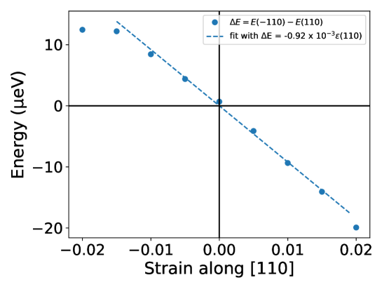
The energy difference between the configuration with magnetic moments oriented along the [10] direction E(10) and along [110] direction E(110) were obtained for a number of cells strained along the [110] direction. Here, a positive value of indicates that the configuration with magnetic moments oriented along the [110] direction are stable while for negative values configurations with [10] are energetically favorable - see Supplementary Fig. 1. The linear fit results in eV per one percent of magnetic anisotropy with strain applied along 110 directions.
Magnetostriction coefficient as well as the magneto-elastic coefficient = 5.1 MPa were also obtained, with the procedure described in detail in Ref. 34.
XMLD-PEEM data on laser assisted Néel vector switching of B-field aligned samples
As described in the main text, the threshold for switching the Néel axis from [110] to in the absence of applied strain was found at mJ/cm2 (see Fig. 3 of the main text). Above threshold, the area of domains aligned parallel to axis further increases, reaching values obtained in the sample aligned under the applied strain along [110] directions (Néel vector aligns perpendicular to the applied tensile strain). The corresponding XMLD-PEEM images of the are before and after irradiation are shown in Supplementary Fig. 2.
Domain structure of laser-aligned sample probed by X-ray magnetic circular dichroism (XMCD)
In addition to the XMLD contrast we recorded X-ray magnetic circular dichroism (XMCD) contrast images of Mn2Au magnetically aligned by laser irradiation under strain. Comparison of the XMCD contrast images with the XMLD contrast images of areas, presented in Supplementary Fig. 3, reveals that all narrow worm-like domains seen in XMLD-PEEM correspond to the 180o domain walls between the two anti-parallel oriented domains.
As shown in Supplementary Fig. 3b, the XMCD contrast gives three distinct color levels in the PEEM image. In this XMCD configuration (see the schematic below the XMCD-PEEM image) the black and the white areas correspond to domains with Néel vectors laying in the plane of incidence of the X-ray beam, aligned anti-parallel to each other. These two domain types are indistinguishable in the XMLD image (Supplementary Fig. 3a). Gray areas in the XMCD-PEEM image correspond to domains with the Néel vector perpendicular to the X-ray propagation direction. For these domains, the exact direction in which the Néel vector is pointing cannot be resolved in this experimental geometry. These two domain types can be, however, distinguished by rotating the sample by 90o (or, alternatively, by changing the propagation direction of the X-ray beam).
In a systematic study of the observed XMCD effect, which will be published elsewhere, the XMCD contrast could be associated with the uncompensated surface moments in Mn2Au.
Schematic description of the thermally-assisted depinning transition
Here we sketch the proposed mechanism of thermally induced DW depinning transition. The depinning transition from a pinned DW (where the DW velocity ) to a sliding DW is realized by increasing the driving force above its threshold value, . Supplementary Fig. 4a presents the schematic dependence of at different temperatures.[26, 27, 28, 29, 30] For simplicity, we neglect the sub-threshold thermally activated creep motion.[30] Supplementary Fig. 4b sketches the effect of optical excitation on DW motion at room temperature, under the applied external force . Here, the resulting transient heating reduces to a value lower than , resulting in DW depinning. Naturally, the threshold fluence (final temperature) to achieve DW depinning depends on , accounting for a difference in threshold fluences in different strain configurations.
Estimates of laser heating effects
When irradiating the sample with a femtosecond laser beam there are several heating effects to be considered. The first is the continuous sample heating, which is proportional to the average irradiation intensity. The continuous laser heating in a thin film is governed by the absorbed light intensity and the thermal properties of the substrate. The temperature increase of the illuminated region can be estimated using a simple steady-state heat diffusion model.[35, 36] Using a reflectivity of 0.52 and the thermal conductivity, , of sapphire at room temperature of 35 W/mK [37] we estimate the steady state heating to be K over the entire range of fluencies used in this experiment. Thus, the continuous laser heating effects can be neglected.
To estimate transient laser heating in a metallic sample, two effects can be considered. On a femtosecond timescale, the rapid electron-electron thermalization leads to a rapid thermalization of the electron gas. Here, assuming no heat transfer to the lattice, the resulting electronic temperature can be estimated considering the absorbed energy per pulse and the electronic specific heat. Considering the calculated electronic density of states in Mn2Au [7] and the Sommerfeld model for the specific heat we obtain the resulting electronic temperatures between 3800 and 6700 K for excitation fluence between 4.2 and 12.6 mJ/cm2. While the optical penetration depth of Mn2Au is estimated to be approximately 30 nm, we assume that the hot electron transport results in a homogeneous electronic temperature throughout the film/buffer layer thickness.
On the timescale of a few picoseconds, the electrons thermalize with the lattice, resulting in a temperature that is governed by the total specific heat of the metallic layer.[25] Under these assumptions, the temperature increase, , is estimated from the absorbed energy density:
Here, is the reflectivity,[10] is the transmission, , are the thicknesses and , are the total specific heats of the corresponding metallic layers. As at temperatures above 300 K the lattice specific heat dominates, we use the Doulong-Petit limit. The resulting temperatures as a function of irradiation fluence are presented in Fig. 2 b. Note that the subsequent cooling of the excited sample volume is governed by the heat diffusion into the substrate, governed by the substrate’s thermal conductivity, . To estimate the evolution of temperature we use a simple heat diffusion model for a semi-infinite solid:[36]
| (6) | ||||
Here = is the thermal diffusivity, is the density of sapphire, is the absorption coefficient and .
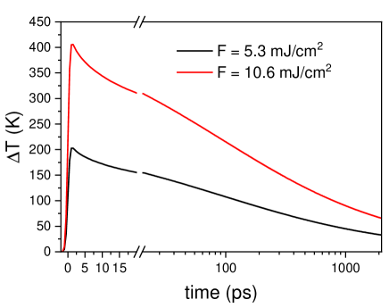
It follows from Supplementary Fig. 5 that the characteristic time, at which drops to one half of its peak value is of the order of 100 ps.