Analytical Theory of Near-Field Electrostatic Effects in Two-Dimensional Materials and van der Waals Heterojunctions
Abstract
We derive and validate a quantitative analytical model of the near-field electrostatic effects in the vicinity (Å) of two-dimensional (2D) materials. In solving the Poisson equation of a near-planar point charge ansatz for the electronic density of a 2D material, our formula quantitatively captures the out-of-plane decay and the in-plane modulation of density functional theory (DFT)-calculated potentials. We provide a method for quickly constructing the electronic density ansatz, and apply it to the case of hexagonal monolayers (BN, AlN, GaN) and monochalcogenides (GeS, GeSe, GeTe, SnS, SnSe, SnTe, PbS, PbSe, PbTe) and their flexural and polar distortions. We demonstrate how our model can be straightforwardly applied to predict material-/angle-specific moiré potentials arising in twisted superlattices with periodicities beyond the reach of DFT calculations.
Two-dimensional (2D) materials are hosts to a variety of desirable electrostatic and electrodynamics effects [1, 2, 3, 4, 5, 6] that make them suitable for plasmonics and photonics applications [7, 8, 9]. In addition to these intrinsic properties, the properties of stacked and substrate-supported 2D materials strongly depends on the near-field (Å) electrostatic interactions between layers. For example, near-field electrostatic interactions in twisted bilayer hexagonal boron nitride (h-BN) [10, 11, 12, 13] and transition metal dichalcogenides [14, 15, 13, 16] can induce macroscopic ferroelectric order, and control the excitonic energy landscape [17, 18, 19, 20, 21]. With the discovery of exotic phenomena in moiré systems [22, 23, 24, 25], accurate continuum models of the interlayer interactions and structural relaxations that connect macroscopic geometric descriptors to microscopic effective low-energy Hamiltonians have been proposed [26, 27, 28, 29], leading to plethora of predictions of exotic electronic states [30, 31, 32, 33, 34]. However, while the near-field electrostatic potential has been extracted from density functional theory (DFT) [35], to the best of our knowledge, no simple closed form of the near-field interactions experienced in 2D materials assemblies or moiré structures has been proposed.
In this work, we derive such an expression for the electrostatic interactions and validate it extensively on DFT calculations. Our formula is obtained solving the Poisson equation for a near-planar discretized ansatz of the 2D materials charge density. We derive this ansatz for two families of 2D materials: hexagonal materials (h-AlN, h-BN, h-GaN) and transition metal monochalcogenides MX (M=Ge, Sn, Pb; X=S, Se, Te), and extract material descriptors for the strength and decay lengths of near-field interactions. At common interlayer distances ( Å), we find that 2D materials can provide large in-plane (V/nm) and out-of-plane ( V/nm) electric fields that both decay exponentially on the scale of the in-plane lattice vectors, effectively reducing the effect of nearest-layer interactions. Our formula also captures the effect of polar and finite-wavevector structural distortions, the latter of which exponentially impacts the electrostatic potential. Finally, we show how our model can easily predict angle-specific moiré potentials for large van der Waals heterostructures with periodicities beyond the reach of DFT calculations.
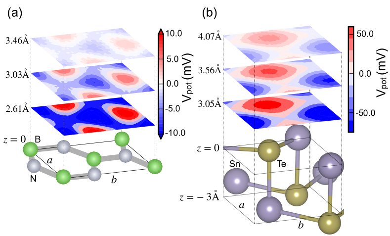
As shown in Fig. 1, 2D material monolayers, such as h-BN and SnTe, induce a modulation of electrostatic potentials at typical 2D-2D and 2D-substrate distances in 2D van der Waals heterostructures (Å and Å for bilayers of h-BN and SnTe, respectively). All DFT parameters and computational details are included in the supplementary information. The potential increases significantly at smaller distances, and decays to negligible values at larger distances ( 5Å) for both 2D materials. In the following and as shown in Fig. 1, we define the coordinates of a point with respect to the plane computed from the averaged atomic coordinates in the top layer (e.g boron and nitrogen are located in the plane for h-BN, and Sn and Te dimers are located near the and Å planes for SnTe). All atomic structures are included in supplementary information.
The magnitude and shape of this in-plane modulation, as well as the lengthscale of its far-field decay, are material-dependent and retain some information of the underlying atomic structure. For example, in the Å plane, the meV in-plane modulation of the electrostatic potential of h-BN has minima (i.e. is most attractive to electrons) close to the positively-charged borons and maxima near the negatively-charged nitrogens, as shown in Fig. 3(a,d). The location of these maxima and minima is weakly impacted by the vertical distance and the exponential [36] decay in the far-field with an out-of-plane decay constant Å-1.
At similar vertical distance of 3.0Å, the in-plane modulation of the potential is an order of magnitude larger (150 meV) in SnTe, with the position of the extrema close to the top-most atoms in the monolayer, see Fig. 2(b,c). The out-of-plane decay constant is also much weaker (Å-1), in accordance with the larger in-plane lattice parameters [36, 12, 35, 37]. This is in agreement with previous works [36, 35, 37] and suggests that the electrostatic potential at such distances can be well approximated by a functional form , with depending on the atomic positions and depending on the lattice parameter and symmetry, which we now derive.
Our derivation consists of two steps: (1) approximate the continuous electronic density of the 2D layer by a set of discrete point charges near the atomic positions, i.e. , and (2) solve the Poisson equation analytically assuming that the vertical fluctuation of these point charges from the plane, , is small compared to , and that . The conditions, and , imply that the monochalcogenide compounds and/or multi-layer 2D materials are approximated by a sum of several neutral slices (e.g. two neutral slices near z=0 and z-3.0Å for SnTe). As discussed more in the next paragraphs and as shown in Fig. 1, the effect of the atoms in the bottom plane of monochalcogenides and/or of multilayer substrates is exponentially weaker and can easily be neglected.
Inspired by atomic representations of electrostatic effects in molecular dynamic simulations [38] and with the objective to reproduce the DFT-calculated electrostatic potential, we determine following the procedure outlined in our previous work on self-assembled molecular layers [37]. In contrast to [37], (i) we set the number of point charges to the number of atoms in a given neutral slice (e.g. 2 point charges per unit cell in h-BN, 2 slices of 2 point charges per unit cell in monochalcogenides), (ii) we allow the point charges in a given slice to be non-planar, as shown in Fig. 2(a), and assigning their position to be at the position of the potential extrema, unlike the model of atomic charges [38]. We refer to this model as discretized charge density (DCD) model. The resulting DCDs for h-BN, h-AlN, h-GaN, and all MX (M=Ge, Sn, Pb; X=S, Se, Te) are reported in Figs. 2(c), 3(d) and the supplementary information. As shown in Fig. S6, the constraint of the in-plane positions of the point charges means they are found close to, but not necessarily at, the atomic locations. In the case of SnTe, as shown in Fig. 2(a-c), the positive and negative point charges are located 0.07Å and 0.16Å away from the Sn and Te atoms, respectively.
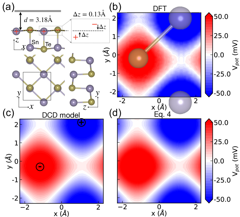
In Fig. 2 (b,c), we show the results from a 2-charge DCD model of SnTe when compared with DFT results of the same structure. As shown in Fig. 2 (c) and in supplementary information for other monochalcogenides, the magnitude of the potential fluctuations and their locations are quantitatively captured by the DCD model, with a mean square deviation on the scale of 0.1meV at d=3.18Å, 0.02 meV at d=4.0Å, 0.01 meV at d=5.0Å, and a mean square deviation of 0.02Å-1 on the decay constant. For reasons elaborated upon below, only charges in the top plane of SnTe are necessary to obtain a quantitative agreement. Results for h-AlN, h-GaN and all monochalcogenides are included in the supplementary information.
With this DCD representation, we can write the potential as the interaction with the point charges and their periodic replica, e.g. (for an orthorhombic lattice of lattice constants a,b) as:
| (1) |
where and are integers to sum over the (infinite number of) periodic images, and is the Coulomb constant.
As shown in the supplementary information and in agreement with our previous work [37], this particular sum converges much faster in reciprocal space. Specifically, the analytical form in reciprocal space for a given neutral plane at a distance is
| (2) |
The first term in the sum corresponds to the areal dipole term identified by Natan et al.[36]. The second sum of runs over the reciprocal lattice points excluding the origin. The lattice parameters and absolute magnitude of are summarized in Table S1 for h-BN, h-AlN, h-GaN and all monochalcogenides.
Eq. 2 is the central result of this work. Unlike its real space expression, this expression converges with a few , allowing us to derive an analytical solution for the potentials from 2D materials. For h-BN, h-AlN, and h-GaN, only 4 terms are necessary to obtain a 99% estimate of the full sum. In the case of monochalcogenides, this value is decreased to 3 terms.
Specifically, writing Eq. 2 for monolayer h-BN, h-AlN, and h-GaN, we obtain,
| (3) |
where . are in fractional coordinates of the atomic positions. is 2.51Å, 3.13Å, and 3.21Å for h-BN, h-AlN, and h-GaN, respectively. We note that the out-of-plane decay for h-BN has been previously reported in the literature [35].
Similarly, for monochalcogenides, Eq. 2 can be simplified to:
| (4) |
where , , are trigonometric functions of (), given in supplementary information. The rapid out-of-plane decay, also explains that only the charges at the top plane contribute appreciably, as this factor decreases the impact of the bottom plane by at d3.18 Å, e.g., the total potential modulation for SnTe at d3.18 Å is 154 meV while the bottom layer only contribute 2.79 meV.
As shown in Fig. 2 (d) and in the supplementary information, despite their simplicity, Eq. 3-Eq. Analytical Theory of Near-Field Electrostatic Effects in Two-Dimensional Materials and van der Waals Heterojunctions are in quantitative agreement with DFT results at distances Å.
Moreover, Eq. 3–Eq. Analytical Theory of Near-Field Electrostatic Effects in Two-Dimensional Materials and van der Waals Heterojunctions have significant implications on the wavelength dependence of structural distortions on near-field interactions. In particular, while the near-field electrostatic effects of the 2D materials decays exponentially with normal distance on a length scale fixed by lattice parameters of the unit cell, the periodic corrugation of the atoms, , only appears in the trigonometric forms and . This implies that periodic corrugation effects, such as infrared(IR)-active phonons at , will only cause a linear change in the near-field potential, while finite wavevector modes will have an exponential effect.
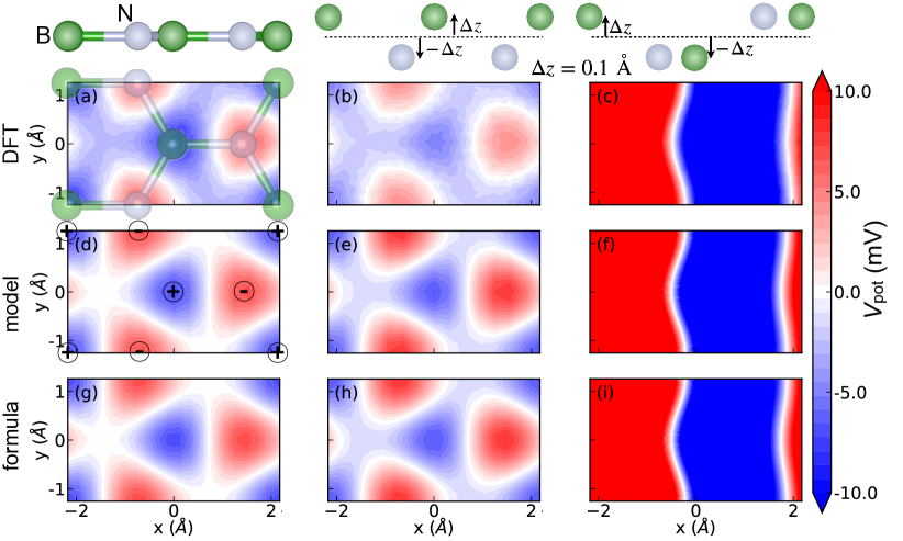
To test this hypothesis, we consider the impact of two different out-of-plane structural distortion modes on the near-field electrostatic potential of h-BN shown in Fig. 3, one corresponding to the q=0 ZO polar mode stabilizing the ferroelectric order in [10, 11, 12, 13], and the other corresponding to a ZA mode at the corner of the Brillouin zone. For illustrative purpose, we consider the same amplitude of displacement ( Å, in the order of out-of-plane atomic displacement in bilayer h-BN at domains of different stackings[11]) while noting that the amplitude along the ZA mode would be larger under thermal occupation. In the right two columns of Fig. 3, we show the atomic structures with out-of-plane displacement of Å and potentials at from the averaged position of the atoms (the black dashed lines). In both cases, the DCD model and analytical formulas (Eq. 3, Eq. S13, Eq. S15) correctly predict the large fluctuation of the near-field potential in response to the finite wavevector (Fig. 3 (e-f), (h-i)), as compared with DFT results (Fig. 3 (b-c)). Fig. 3 also implies that our model can also be used to explore the electrostatic impacts of strain and corrugation in the properties of moiré structures [39, 11].
Fig. 3 further emphasizes the dominant role of the in-plane periodicity in describing the near-field electrostatic potential [36]: the doubling of periodicity in Fig. 3 (c) results in a strong modulation on the shape and the magnitude of the potential fluctuation. When compared to Fig. 3 (b), at equal amplitude of distortion and at Å, the modulation is about five times larger (potential fluctuation is 14 meV in Fig. 3 (b) vs. 68 meV in Fig. 3 (c)), and the potential becomes quasi-one-dimensional. We also note that, while the magnitude of the point charge impacts the potential, the effect is also only linear and can be neglected as compared to the effects of lattice parameters (SnTe has much larger potential modulation than h-BN, despite for SnTe and for h-BN, see Table S1).
With this framework, we finally demonstrate how our analytical formulas can be used to predict moiré potential superlattices for twisted van der Waals heterostructures, which are challenging for DFT calculations due to the large number of atoms in the unit cell. We note that we are neglecting the structural relaxations that robust models have been already proposed and validated [26, 27], and focus solely on the electrostatic component in the following. Under these assumptions, the moiré potential can be obtained by a simple rotation of the atomic coordinates in one of the layers, i.e. by solely modifying the trigonometric forms and in Eq. 3 and Eq. Analytical Theory of Near-Field Electrostatic Effects in Two-Dimensional Materials and van der Waals Heterojunctions for hexagonal monolayers and monochalcogenides, respectively.
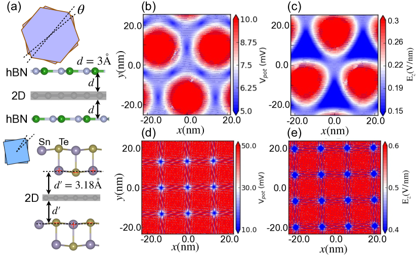
We adopt a heterostructure configuration that has demonstrated exotic property control by the twist angle of the top and bottom layer[40, 41], as shown in Fig. 4(a) and compute the potential experienced by a central planar 2D material, surrounded by top and bottom h-BN or SnTe. When the two h-BN layers are twisted by angle , the potential becomes:
| (5) |
where with same as that in Eq.3 and . This also allows us to compute the resulting electric field (Eq. S24). In Fig. 4 we present the in-plane potential and out-of-plane electric field at the center 2D layer for h-BN with rotation angle and SnTe with . The twisted bilayer h-BN generates a moiré potential superlattices with wavelength on the order of 30nm at , a lengthscale challenging for DFT calculations. As 2D materials can be controlled and manipulated via potential modulations or external electric fields[42, 43, 44, 45, 37], our simple analytical model for near-field electrostatic effects of layered 2D materials can be used for study the electronic and optical response of various moiré potential superlattices.
In summary, we have derived a novel material-specific analytical theory of the large near-field electrostatic effects in 2D materials. Our theory fully captures the magnitude of the potential modulations (on the order of mV for h-BN and mV for monochalcogenides) at typical interlayer distances (3Å 4Å) of van der Waals layered structures, as well as the out-of-plane decay of these fluctuations. We parametrized a discretized charge density model to reproduce DFT-calculated potentials for two classes of 2D materials. Importantly, our formula is predictive and elucidates the importance of in-plane lattice constants, geometric effects, structural distortions, corrugation, distance, and material polarity in the electrostatic potential. Furthermore, our formula can be used to compute an analytical expression of the angle-specific moiré potentials and electric fields on lengthscales on the order of tens to hundreds of nanometers, which are challenging for DFT calculations.
Supplementary Material
Details of the computational methods, including the details for DFT calculations, and the DCD model; Results of the electrostatic potential for h-AlN, h-GaN and all monochalcogenides from DFT, DCD model and analytical formula; Potential fluctuations as a function of distance for all 2D materials from DFT, DCD model and analytical formula;
Structures of the 2D materials in crystallographic information file (cif) format.
Acknowledgments
This work was supported by the Northwestern University MRSEC under National Science Foundation grant No. DMR-1720139 (Q.Z., P.D.). Work performed at the Center for Nanoscale Materials, a U.S. Department of Energy Office of Science User Facility, was supported by the U.S. DOE, Office of Basic Energy Sciences, under Contract No. DE-AC02-06CH11357. We gratefully acknowledge use of the Bebop cluster in the Laboratory Computing Resource Center at Argonne National Laboratory. P.D. would like to acknowledge fruitful discussions with Cristian Cortès, Lincoln Lauhon, and Mark Hersam.
References
- Alcaraz Iranzo et al. [2018] D. Alcaraz Iranzo, S. Nanot, E. J. Dias, I. Epstein, C. Peng, D. K. Efetov, M. B. Lundeberg, R. Parret, J. Osmond, J.-Y. Hong, et al., Probing the ultimate plasmon confinement limits with a van der waals heterostructure, Science 360, 291 (2018).
- da Jornada et al. [2020] F. H. da Jornada, L. Xian, A. Rubio, and S. G. Louie, Universal slow plasmons and giant field enhancement in atomically thin quasi-two-dimensional metals, Nature communications 11, 1 (2020).
- Koppens et al. [2011] F. H. Koppens, D. E. Chang, and F. J. Garcia de Abajo, Graphene plasmonics: a platform for strong light–matter interactions, Nano letters 11, 3370 (2011).
- Ghosh et al. [2017] B. Ghosh, P. Kumar, A. Thakur, Y. S. Chauhan, S. Bhowmick, and A. Agarwal, Anisotropic plasmons, excitons, and electron energy loss spectroscopy of phosphorene, Physical Review B 96, 035422 (2017).
- Huang et al. [2017] Y. Huang, S. N. Shirodkar, and B. I. Yakobson, Two-dimensional boron polymorphs for visible range plasmonics: a first-principles exploration, Journal of the American Chemical Society 139, 17181 (2017).
- Lian et al. [2020] C. Lian, S.-Q. Hu, J. Zhang, C. Cheng, Z. Yuan, S. Gao, and S. Meng, Integrated plasmonics: Broadband dirac plasmons in borophene, Physical Review Letters 125, 116802 (2020).
- Low and Avouris [2014] T. Low and P. Avouris, Graphene plasmonics for terahertz to mid-infrared applications, ACS Nano 8, 1086 (2014).
- Xia et al. [2014] F. Xia, H. Wang, D. Xiao, M. Dubey, and A. Ramasubramaniam, Two-dimensional material nanophotonics, Nature Photonics 8, 899 (2014).
- Ju et al. [2011] L. Ju, B. Geng, J. Horng, C. Girit, M. Martin, Z. Hao, H. A. Bechtel, X. Liang, A. Zettl, Y. R. Shen, et al., Graphene plasmonics for tunable terahertz metamaterials, Nature nanotechnology 6, 630 (2011).
- Yasuda et al. [2021] K. Yasuda, X. Wang, K. Watanabe, T. Taniguchi, and P. Jarillo-Herrero, Stacking-engineered ferroelectricity in bilayer boron nitride, Science 372, 1458 (2021).
- Stern et al. [2021] M. V. Stern, Y. Waschitz, W. Cao, I. Nevo, K. Watanabe, T. Taniguchi, E. Sela, M. Urbakh, O. Hod, and M. B. Shalom, Interfacial ferroelectricity by van der waals sliding, Science 372, 1462 (2021).
- Woods et al. [2021] C. Woods, P. Ares, H. Nevison-Andrews, M. Holwill, R. Fabregas, F. Guinea, A. Geim, K. Novoselov, N. Walet, and L. Fumagalli, Charge-polarized interfacial superlattices in marginally twisted hexagonal boron nitride, Nature communications 12, 1 (2021).
- Li and Wu [2017] L. Li and M. Wu, Binary compound bilayer and multilayer with vertical polarizations: two-dimensional ferroelectrics, multiferroics, and nanogenerators, ACS nano 11, 6382 (2017).
- Wang et al. [2022] X. Wang, K. Yasuda, Y. Zhang, S. Liu, K. Watanabe, T. Taniguchi, J. Hone, L. Fu, and P. Jarillo-Herrero, Interfacial ferroelectricity in rhombohedral-stacked bilayer transition metal dichalcogenides, Nature nanotechnology , 1 (2022).
- Weston et al. [2022] A. Weston, E. G. Castanon, V. Enaldiev, F. Ferreira, S. Bhattacharjee, S. Xu, H. Corte-León, Z. Wu, N. Clark, A. Summerfield, et al., Interfacial ferroelectricity in marginally twisted 2d semiconductors, Nature Nanotechnology , 1 (2022).
- Wu [2021] M. Wu, Two-dimensional van der waals ferroelectrics: Scientific and technological opportunities, ACS nano 15, 9229 (2021).
- Yu et al. [2015] H. Yu, Y. Wang, Q. Tong, X. Xu, and W. Yao, Anomalous light cones and valley optical selection rules of interlayer excitons in twisted heterobilayers, Physical review letters 115, 187002 (2015).
- Wilson et al. [2021] N. P. Wilson, W. Yao, J. Shan, and X. Xu, Excitons and emergent quantum phenomena in stacked 2d semiconductors, Nature 599, 383 (2021).
- Zhang et al. [2020] L. Zhang, Z. Zhang, F. Wu, D. Wang, R. Gogna, S. Hou, K. Watanabe, T. Taniguchi, K. Kulkarni, T. Kuo, et al., Twist-angle dependence of moiré excitons in ws2/mose2 heterobilayers, Nature communications 11, 1 (2020).
- Miller et al. [2017] B. Miller, A. Steinhoff, B. Pano, J. Klein, F. Jahnke, A. Holleitner, and U. Wurstbauer, Long-lived direct and indirect interlayer excitons in van der waals heterostructures, Nano letters 17, 5229 (2017).
- Shabani et al. [2021] S. Shabani, D. Halbertal, W. Wu, M. Chen, S. Liu, J. Hone, W. Yao, D. N. Basov, X. Zhu, and A. N. Pasupathy, Deep moiré potentials in twisted transition metal dichalcogenide bilayers, Nature Physics 17, 720 (2021).
- Cao et al. [2018] Y. Cao, V. Fatemi, S. Fang, K. Watanabe, T. Taniguchi, E. Kaxiras, and P. Jarillo-Herrero, Unconventional superconductivity in magic-angle graphene superlattices, Nature 556, 43 (2018).
- Yankowitz et al. [2019] M. Yankowitz, S. Chen, H. Polshyn, Y. Zhang, K. Watanabe, T. Taniguchi, D. Graf, A. F. Young, and C. R. Dean, Tuning superconductivity in twisted bilayer graphene, Science 363, 1059 (2019).
- Park et al. [2021a] J. M. Park, Y. Cao, K. Watanabe, T. Taniguchi, and P. Jarillo-Herrero, Tunable strongly coupled superconductivity in magic-angle twisted trilayer graphene, Nature 590, 249 (2021a).
- Park et al. [2021b] J. M. Park, Y. Cao, K. Watanabe, T. Taniguchi, and P. Jarillo-Herrero, Flavour hund’s coupling, chern gaps and charge diffusivity in moiré graphene, Nature 592, 43 (2021b).
- Carr et al. [2019] S. Carr, S. Fang, Z. Zhu, and E. Kaxiras, Exact continuum model for low-energy electronic states of twisted bilayer graphene, Physical Review Research 1, 013001 (2019).
- Tang et al. [2021] H. Tang, S. Carr, and E. Kaxiras, Geometric origins of topological insulation in twisted layered semiconductors, Physical Review B 104, 155415 (2021).
- Angeli and MacDonald [2021] M. Angeli and A. H. MacDonald, valley transition metal dichalcogenide moiré bands, Proceedings of the National Academy of Sciences 118 (2021).
- Quan et al. [2021] J. Quan, L. Linhart, M.-L. Lin, D. Lee, J. Zhu, C.-Y. Wang, W.-T. Hsu, J. Choi, J. Embley, C. Young, et al., Phonon renormalization in reconstructed mos2 moiré superlattices, Nature Materials 20, 1100 (2021).
- Wu et al. [2018] F. Wu, T. Lovorn, E. Tutuc, and A. H. MacDonald, Hubbard model physics in transition metal dichalcogenide moiré bands, Physical review letters 121, 026402 (2018).
- Wu et al. [2019] F. Wu, T. Lovorn, E. Tutuc, I. Martin, and A. MacDonald, Topological insulators in twisted transition metal dichalcogenide homobilayers, Physical review letters 122, 086402 (2019).
- Xian et al. [2019] L. Xian, D. M. Kennes, N. Tancogne-Dejean, M. Altarelli, and A. Rubio, Multiflat bands and strong correlations in twisted bilayer boron nitride: Doping-induced correlated insulator and superconductor, Nano letters 19, 4934 (2019).
- Pan et al. [2020] H. Pan, F. Wu, and S. D. Sarma, Band topology, hubbard model, heisenberg model, and dzyaloshinskii-moriya interaction in twisted bilayer wse 2, Physical Review Research 2, 033087 (2020).
- Kennes et al. [2021] D. M. Kennes, M. Claassen, L. Xian, A. Georges, A. J. Millis, J. Hone, C. R. Dean, D. Basov, A. N. Pasupathy, and A. Rubio, Moiré heterostructures as a condensed-matter quantum simulator, Nature Physics 17, 155 (2021).
- Zhao et al. [2021] P. Zhao, C. Xiao, and W. Yao, Universal superlattice potential for 2d materials from twisted interface inside h-bn substrate, npj 2D Materials and Applications 5, 1 (2021).
- Natan et al. [2007] A. Natan, L. Kronik, H. Haick, and R. T. Tung, Electrostatic properties of ideal and non-ideal polar organic monolayers: Implications for electronic devices, Adv. Mater. 19, 4103 (2007).
- Zhou et al. [2021] Q. Zhou, B. Anaclet, T. Steiner, M. Kotiuga, and P. Darancet, Engineering the electronic structure of two-dimensional materials with near-field electrostatic effects of self-assembled organic layers, arXiv preprint arXiv:2109.09990 (2021).
- Wang et al. [2014] B. Wang, S. L. Li, and D. G. Truhlar, Modeling the partial atomic charges in inorganometallic molecules and solids and charge redistribution in lithium-ion cathodes, Journal of Chemical Theory and Computation 10, 5640 (2014).
- Li et al. [2021a] H. Li, S. Li, M. H. Naik, J. Xie, X. Li, J. Wang, E. Regan, D. Wang, W. Zhao, S. Zhao, et al., Imaging moiré flat bands in three-dimensional reconstructed wse2/ws2 superlattices, Nature materials 20, 945 (2021a).
- Ribeiro-Palau et al. [2018] R. Ribeiro-Palau, C. Zhang, K. Watanabe, T. Taniguchi, J. Hone, and C. R. Dean, Twistable electronics with dynamically rotatable heterostructures, Science 361, 690 (2018).
- Sun et al. [2021] X. Sun, S. Zhang, Z. Liu, H. Zhu, J. Huang, K. Yuan, Z. Wang, K. Watanabe, T. Taniguchi, X. Li, et al., Correlated states in doubly-aligned hbn/graphene/hbn heterostructures, Nature Communications 12, 1 (2021).
- Park et al. [2008a] C.-H. Park, L. Yang, Y.-W. Son, M. L. Cohen, and S. G. Louie, Anisotropic behaviours of massless dirac fermions in graphene under periodic potentials, Nat. Phys. 4, 213 (2008a).
- Park et al. [2008b] C.-H. Park, L. Yang, Y.-W. Son, M. L. Cohen, and S. G. Louie, New generation of massless dirac fermions in graphene under external periodic potentials, Phys. Rev. Lett. 101, 126804 (2008b).
- Li et al. [2021b] Y. Li, S. Dietrich, C. Forsythe, T. Taniguchi, K. Watanabe, P. Moon, and C. R. Dean, Anisotropic band flattening in graphene with one-dimensional superlattices, Nature Nanotechnology 16, 525 (2021b).
- Morrow and Ma [2021] D. J. Morrow and X. Ma, Trapping interlayer excitons in van der waals heterostructures by potential arrays, Physical Review B 104, 195302 (2021).