Electrical switching of a moiré ferroelectric superconductor
Electrical control of superconductivity is critical for nanoscale superconducting circuits including cryogenic memory elements [1, 2, 3, 4], superconducting field-effect transistors (FETs) [5, 6, 7], and gate-tunable qubits [8, 9, 10]. Superconducting FETs operate through continuous tuning of carrier density, but there has not yet been a bistable superconducting FET, which could serve as a new type of cryogenic memory element. Recently, unusual ferroelectricity in Bernal-stacked bilayer graphene aligned to its insulating hexagonal boron nitride (BN) gate dielectrics was discovered [11]. Here, we report the observation of ferroelectricity in magic-angle twisted bilayer graphene (MATBG) with aligned BN layers. This ferroelectric behavior coexists alongside the strongly correlated electron system of MATBG without disrupting its correlated insulator or superconducting states. This all-van der Waals platform enables configurable switching between different electronic states of this rich system. To illustrate this new approach, we demonstrate reproducible bistable switching between the superconducting, metallic, and correlated insulator states of MATBG using gate voltage or electric displacement field. These experiments unlock the potential to broadly incorporate this new moiré ferroelectric superconductor into highly tunable superconducting electronics.
Twisting two layers of graphene forms a moiré superlattice with alternating regions of AA and AB/BA stacking. Near the magic angle of 1.1, interlayer hybridization at the AA regions leads to renormalized flat energy bands [12, 13, 14, 15, 16], thereby suppressing the electronic kinetic energy and enabling strong Coulomb interactions to dominate. Experimental realizations of MATBG have led to a number of surprising results including the discovery of superconductivity [17], correlated insulating states [18], orbital magnetism and the quantum anomalous Hall effect [19, 20], and strange metal behavior [21]. Beyond MATBG, a new field of twistronics has begun to explore the effects of moiré superlattices in other van der Waals crystals. Researchers have investigated moiré patterns in twisted bilayers of BN at small twist angles [22, 23], resulting in ferroelectricity (FE) due to a shift in the ionic dipole from the boron and nitrogen ions. Surprisingly, ferroelectricity has also been observed in a double moiré system from the alignment of the BN layers sandwiching Bernal-stacked AB bilayer graphene [11]. In this work, we present the discovery of ferroelectric behavior in MATBG, in which the top and bottom BN crystallographic edges are closely aligned to one another modulo 30.
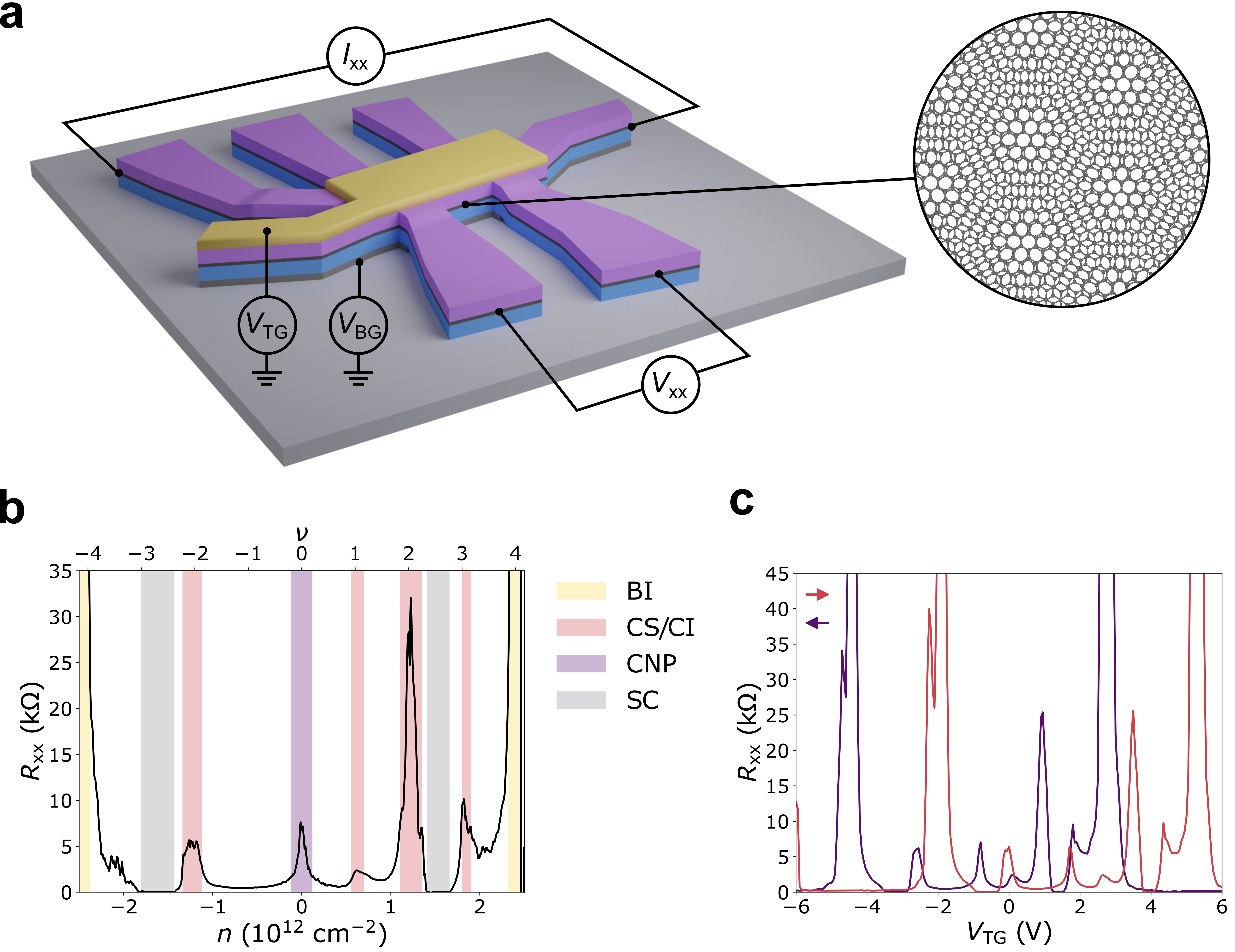
The stack was fabricated using standard cut-and-stack dry-transfer van der Waals assembly (see Methods). The final device, shown schematically in Fig. 1a, is etched into a Hall bar geometry with a metal (Cr/Au) top gate and local few-layer graphite bottom gate. During van der Waals assembly, the long, sharp crystallographic edges of the top and bottom BN flakes were intentionally aligned to one another, resulting in the two BN layers approximately aligned modulo 30 (see Fig. S1).
Low-temperature transport measurements demonstrate the expected features of a high-quality twisted bilayer graphene device close to the magic angle . In Fig. 1b, the four-probe longitudinal resistance is plotted as a function of carrier density using the local graphite bottom gate () at a base mixing chamber temperature of 40 mK. The filling factor refers to the number of electrons or holes per MATBG moiré superlattice unit cell; = 4 refer to full filling of the moiré bands with four electrons or holes per unit cell, respectively. The transport data show prominent resistive features corresponding to the charge neutrality point (CNP, = 0), band insulating peaks (BI, = 4), and correlated semimetal/insulating peaks (CS/CI, = 1, 2, 3). Moreover, robust superconducting (SC) regions appear near half-filling of the moiré unit cell at = . A twist angle of 1.03 can be extracted from the CNP and = 2 peak (see Methods).
Strikingly, when the top gate is instead used to tune the carrier density in the device, there is a large hysteretic shift in the transport features of MATBG depending on the sweep direction of (Fig. 1c). When the gate voltage is initially swept, there is a large region over which the gate appears to not work, followed by a region of expected behavior where the MATBG carrier density is changing. This observation is consistent with the proposed picture of “layer-specific anomalous screening” (LSAS) described in Ref. [11].
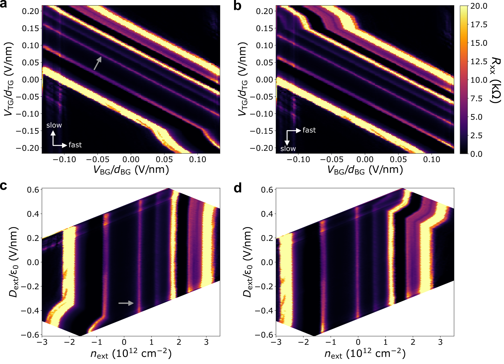
To further investigate this emergent ferroelectric behavior in our MATBG device, we performed dual-gate maps of as a function of both gate voltages. We show the effects of sweeping the top gate as the slow axis either from negative to positive voltage (Fig. 2a) or from positive to negative voltage (Fig. 2b). When is initially changed, the transport features gradually evolve, suggesting that the gate is not fully introducing carriers into the MATBG layers as would be expected in a standard field-effect transistor. Upon further modulation of , the device abruptly enters the familiar regime where the resistive peaks, which occur at constant carrier density in MATBG, follow straight-line trajectories in the dual-gate plane. This change in behavior can be visualized more easily using converted axes in Fig. 2c (converted from Fig. 2a) and 2d (converted from Fig. 2b). The transformation is defined as: , . In the regions where the top gate is adding carriers to the MATBG device by the expected amount, the transport features follow vertical-line trajectories, in agreement with previous observations that the strongly correlated electron system in MATBG is independent of displacement field [19].
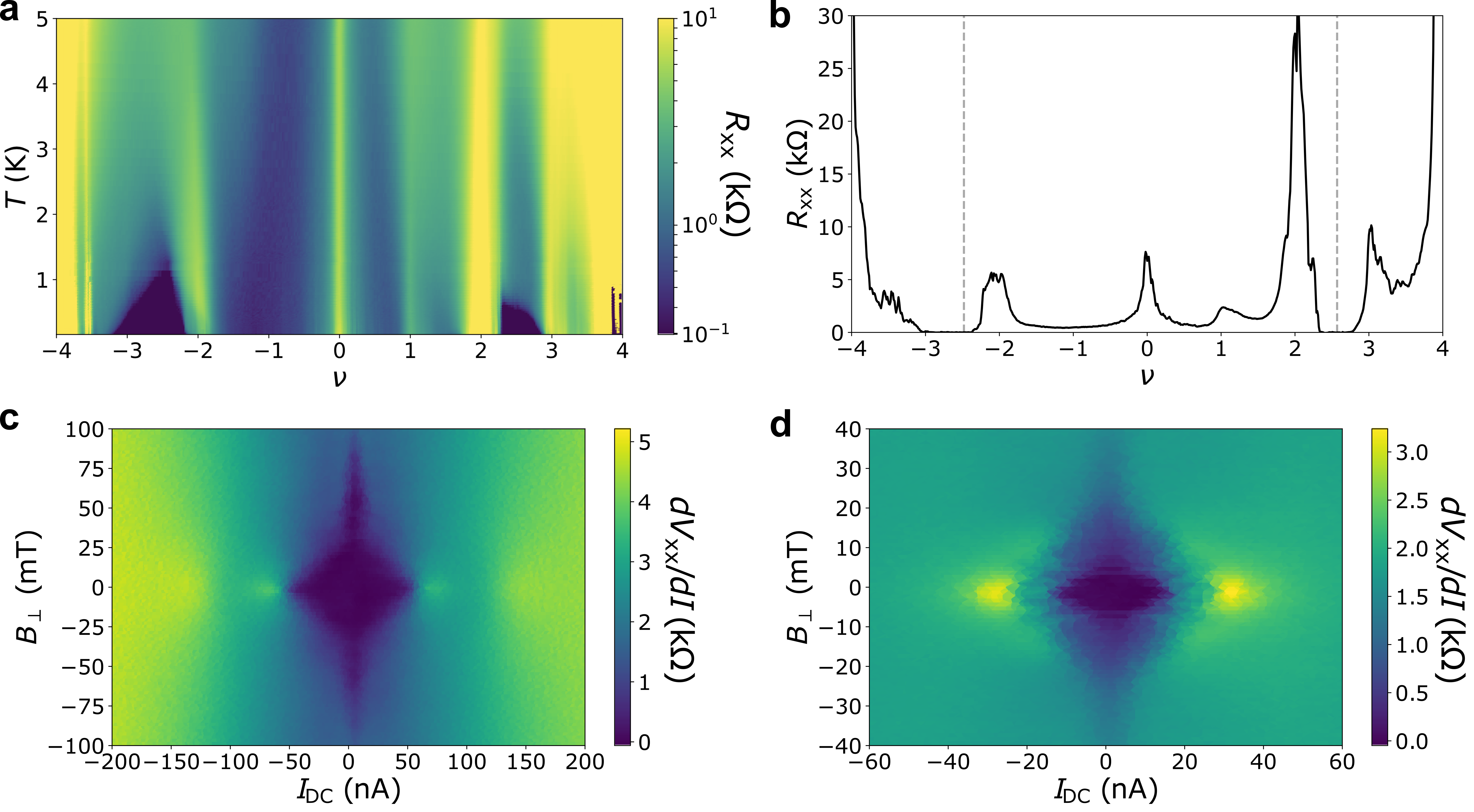
Based on our dual-gate observations in Fig. 2, we conclude that the emergent ferroelectricity in our device persists alongside the strongly correlated behavior of MATBG. To confirm this coexistence, we study the superconductivity in our device in one of its two bistable configurations. In Fig. 3a, we plot the four-probe as a function of bottom gate and temperature. Two superconducting domes appear at = , in agreement with prior MATBG phenomenology. Using the definition of critical temperature as 50% of the normal state resistance (see Supplemental Information), we extract maximal of 2.15 K () and 0.83 K () for the hole and electron domes, respectively.
The superconductivity remains prominent over large regions on both the electron and hole sides at = (Fig. 3b). Using the bottom gate, we can park the system in either region at fixed carrier density. In Fig. 3c, we show the differential resistance as a function of both DC current and applied perpendicular magnetic field on the hole side at . We find that the superconducting critical current is maximized at = 0 and falls to zero with increasing approaching mT. We find similar results on the electron side at (Fig. 3d), with the critical current vanishing near = mT. These data are hallmarks of robust superconductivity persisting in MATBG and, importantly, are not influenced by the coexisting FE behavior. The underlying mechanism of the ferroelectricity now observed in both Bernal bilayer graphene and MATBG sandwiched by aligned BN dielectrics is still not understood. These results in MATBG provide valuable evidence in developing an understanding of where the ferroelectricity lies, given its clear lack of interplay with the strongly interacting electrons in the MATBG moiré superlattice.
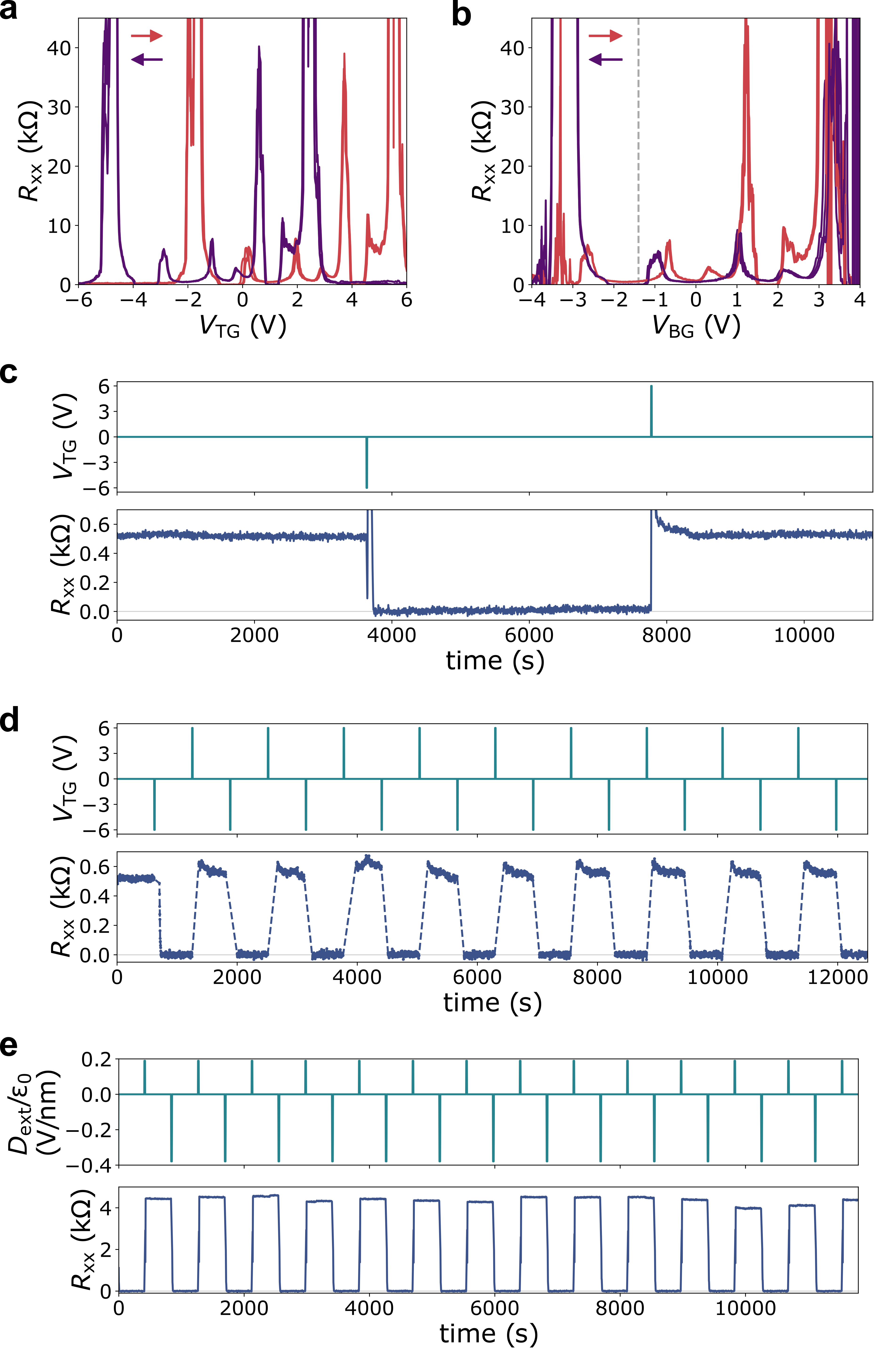
The FE hysteresis persists upon cycling between the two hysteretic sweep directions. In Fig. 4a, is shown when the top gate is swept back and forth from 6 V over six traces. A clear bistability emerges: the up and down traces occur at the same positions depending only on sweep direction. Furthermore, the history of the applied top gate also influences the bottom gate sweeps. We can prepare the system in either state by setting = 0, applying = 6 V for several seconds, and then setting back to 0. Next, we set = 4 V and sweep the bottom gate. This sign is chosen to maintain the same sign of at the start of each scan. As shown in Fig. 4b, the system is again bistable when this sequence is repeated over six traces.
Now that we have established the coexistence of a FE bistability and strongly correlated MATBG behavior in a single device, we can make use of this property to reversibly switch between different electronic states. In Fig. 4c, we initially prepare the system with a pulse of = 6 V before setting = 0. We then fix the applied bottom gate at 1.4 V, placing the system in the hole-side () superconducting phase. Remarkably, we demonstrate switching of from this superconducting state to a stable metallic state after applying a pulse of = 6 V and setting the top gate back to 0 (Fig. 4c). After pausing in the metallic state, we then apply a second pulse of = 6 V to return the device to the superconducting state. In order to emphasize the stability of this procedure, we also perform a pulsed sequence of alternating = 6 V pulses to repeatably switch the system between the bistable superconducting and metallic states at a fixed bottom gate voltage (Fig. 4d).
Moreover, we also demonstrate the capability to switch between different electronic phases of MATBG at fixed applied carrier density using only applied displacement field. Employing the definitions of and stated earlier, we fix the system at = . Next, using alternating pulses of = 0.189 V/nm and -0.379 V/nm, we show the capacity to switch between superconducting and resistive correlated insulator states (Fig. 4e). This repeatability reflects the robust FE behavior existing in this system and illustrates its utility as a novel van der Waals platform for superconducting switches.
Past research on controlling superconductivity has primarily focused on FETs to continuously tune carrier density, thereby inducing superconductivity in oxide thin films [24, 25] and ultrathin van der Waals crystals [26, 7, 17]. However, these devices rely on a continuous change in an applied gate voltage rather than a discrete switch between two stable states. Furthermore, they typically require much larger carrier densities ( cm-2) than the low-density SC in MATBG ( cm-2) owing to the large area of the MATBG moiré unit cell. Other types of experiments have successfully turned superconductivity on and off using light pulses [27, 28] or applied magnetic fields [29], but these are limited in their applicability compared to electrical control. Previous work employing both ferroelectricity and superconductivity using thin film FE oxides show modulation of with FE polarization, but do not report controllable switching behavior between superconducting and other electronic phases at fixed temperature [30, 31]. The data presented in this letter thus mark the first example of a nonvolatile FE SC FET.
To summarize, our results introduce a highly tunable all-van der Waals platform to enact bistable ferroelectric switching between a range of electronic states in a strongly correlated electron system at low carrier density. Recent progress in moiré superconducting devices using patterned electrostatic gating of MATBG with BN dielectrics has achieved Josephson junctions [32, 33], including magnetic Josephson junctions [34], superconducting diodes [34], and superconducting quantum interference devices (SQUIDS) [35]. These van der Waals heterostructures, constructed from a single material platform, bypass the issues of strain and disorder that often occur at the interfaces between different thin films. Combining the bistable ferroelectric switching demonstrated here with configurable Josephson junction geometries will enable an additional control knob over the electronic states, paving the way for a new generation of moiré graphene superconducting electronics.
Methods
Device fabrication. The van der Waals heterostructure was assembled in two parts using standard dry transfer techniques. First, a poly(bisphenol A carbonate) stamp was used to pick up a hexagonal boron nitride (BN) flake and few-layer graphite strip. This bottom gate stack was placed on a 285 nm SiO2/Si substrate and annealed to remove any residue. Next, a large monolayer graphene flake was cut into two pieces using a laser setup described in Ref. [36]. A second stamp was used to pick up a top BN flake using heat. At room temperature, the stamp then picked up one monolayer, the stage was rotated by 1.1, and then the stamp picked up the other half. Finally, the stack was released onto the bottom gate stack with alignment of the long, sharp edges of the two BN layers serving as the gate dielectrics. These edges are likely either zigzag or armchair terminations of the crystal lattice. Thus, the BN layers are crystallographically aligned modulo 30.
A metallic top gate of Cr/Au (5/40 nm) was deposited and the device was etched into a Hall bar geometry using reactive ion etching. The MATBG layers were contacted using a combined etch and evaporation of Cr/Au (5/40 nm) metallic contacts.
Transport measurements. Low-temperature electrical transport measurements were carried out in a dilution refrigerator with a perpendicular superconducting magnet. The sample current and four-probe voltage were measured using SR-830 lock-in amplifiers with pre-amplifier gains of and 10, respectively. The lock-ins were synchronized at a frequency of 7-8 Hz and an AC excitation current of 1 nA was applied. For the temperature dependent measurements in Fig. 3a and supplemental data, an on-chip thermometer (Lakeshore RX-102A-BR) was employed.
Twist angle determination. The twist angle of the MATBG device can be extracted from the positions of the insulating peaks as a function of carrier density using the bottom gate. We can obtain the carrier density = ()(/), where we take = 3.5. Full filling of the moiré superlattice occurs for , where the lattice constant = 0.246 nm for graphene. The value was calculated using the positions of insulating peaks at = 0 and 2.
Acknowledgements
The authors acknowledge Qiong Ma and Zhiren Zheng for helpful discussions. This work was supported by the Air Force Office of Scientific Research (AFOSR) 2DMAGIC MURI FA9550-19-1-0390 (D.R.K. and L.-Q.X.), the Army Research Office MURI W911NF2120147 (D.M.), as well as the Gordon and Betty Moore Foundation’s EPiQS Initiative through grant GBMF9463 to P.J.-H. K.W. and T.T. acknowledge support from the Elemental Strategy Initiative conducted by the MEXT, Japan (JPMXP0112101001), JSPS KAKENHI (JP20H00354), and the CREST(JPMJCR15F3), JST. This work made use of the MIT MRSEC Shared Experimental Facilities, supported by the NSF (DMR-0819762), and of Harvard’s Center for Nanoscale Systems, supported by the NSF (ECS-0335765).
References
- [1] B. Baek, W. H. Rippard, S. P. Benz, S. E. Russek, and P. D. Dresselhaus. Hybrid superconducting-magnetic memory device using competing order parameters. Nat. Commun., 5:3888, 2014.
- [2] E. C. Gingrich, B. M. Niedzielski, J. A. Glick, Y. Wang, D. L. Miller, R. Loloee, W. P. Pratt Jr., and N. O. Birge. Controllable - Josephson junctions containing a ferromagnetic spin valve. Nat. Phys., 12:564–567, 2016.
- [3] K. Sardashti, M. C. Dartiailh, J. Yuan, S. Hart, P. Gumann, and J. Shabani. Voltage-Tunable Superconducting Resonators: A Platform for Random Access Quantum Memory. IEEE Trans. Quantum Eng., 1:1–7, 2020.
- [4] S. Alam, M. S. Hossain, S. R. Srinivasa, and A. Aziz. Cryogenic Memory Technologies. arXiv, 2021.
- [5] Y.-J. Doh, J. A. van Dam, A. L. Roest, E. P. A. M. Bakkers, L. P. Kouwenhoven, and S. De Franceschi. Tunable Supercurrent Through Semiconductor Nanowires. Science, 309:272–275, 2005.
- [6] G. De Simoni, F. Paolucci, P. Solinas, E. Strambini, and F. Giazotto. Metallic supercurrent field-effect transistor. Nat. Nanotechnol., 13:802–805, 2018.
- [7] V. Fatemi, S. Wu, Y. Cao, L. Bretheau, Q. D. Gibson, K. Watanabe, T. Taniguchi, R. J. Cava, and P. Jarillo-Herrero. Electrically tunable low-density superconductivity in a monolayer topological insulator. Science, 362:926–929, 2018.
- [8] T. W. Larsen, K. D. Petersson, F. Kuemmeth, T. S. Jespersen, P. Krogstrup, J. Nygård, and C. M. Marcus. Semiconductor-Nanowire-Based Superconducting Qubit. Phys. Rev. Lett., 115:127001, 2015.
- [9] G. de Lange, B. van Heck, A. Bruno, D. J. van Woerkom, A. Geresdi, S. R. Plissard, E. P. A. M. Bakkers, A. R. Akhmerov, and L. DiCarlo. Realization of Microwave Quantum Circuits Using Hybrid Superconducting-Semiconducting Nanowire Josephson Elements. Phys. Rev. Lett., 115:127002, 2015.
- [10] J. I.-J. Wang, D. Rodan-Legrain, L. Bretheau, D. L. Campbell, B. Kannan, D. Kim, M. Kjaergaard, P. Krantz, G. O. Samach, F. Yan, J. L. Yoder, K. Watanabe, T. Taniguchi, T. P. Orlando, S. Gustavsson, P. Jarillo-Herrero, and W. D. Oliver. Coherent control of a hybrid superconducting circuit made with graphene-based van der Waals heterostructures. Nat. Nanotechnol., 14:120–125, 2019.
- [11] Z. Zheng, Q. Ma, Z. Bi, S. de la Barrera, M.-H. Liu, N. Mao, Y. Zhang, N. Kiper, K. Watanabe, T. Taniguchi, J. Kong, W. A. Tisdale, R. Ashoori, N. Gedik, L. Fu, S.-Y. Xu, and P. Jarillo-Herrero. Unconventional ferroelectricity in moiré heterostructures. Nature, 588:71–76, 2020.
- [12] E. Suárez Morell, J. D. Correa, P. Vargas, M. Pacheco, and Z. Barticevic. Flat bands in slightly twisted bilayer graphene: Tight-binding calculations. Phys. Rev. B, 82:121407(R), 2010.
- [13] R. Bistritzer and A. H. MacDonald. Moiré bands in twisted double-layer graphene. Proc. Natl. Acad. Sci. U.S.A., 108:12233–12237, 2011.
- [14] J. M. B. Lopes dos Santos, N. M. R. Peres, and A. H. Castro Neto. Continuum model of the twisted graphene bilayer. Phys. Rev. B, 86:155449, 2012.
- [15] G. Li, A. Luican, J. M. B. Lopes dos Santos, A. H. Castro Neto, A. Reina, J. Kong, and E. Y. Andrei. Observation of Van Hove singularities in twisted graphene layers. Nat. Phys., 6:109–113, 2010.
- [16] A. Luican, G. Li, A. Reina, J. Kong, R. R. Nair, K. S. Novoselov, A. K. Geim, and E. Y. Andrei. Single-Layer Behavior and Its Breakdown in Twisted Graphene Layers. Phys. Rev. Lett., 106:126802, 2011.
- [17] Y. Cao, V. Fatemi, S. Fang, K. Watanabe, T. Taniguchi, E. Kaxiras, and P. Jarillo-Herrero. Unconventional superconductivity in magic-angle graphene superlattices. Nature, 556:43–50, 2018.
- [18] Y. Cao, V. Fatemi, A. Demir, S. Fang, S. L. Tomarken, J. Y. Luo, J. D. Sanchez-Yamagishi, K. Watanabe, T. Taniguchi, E. Kaxiras, R. C. Ashoori, and P. Jarillo-Herrero. Correlated insulator behaviour at half-filling in magic-angle graphene superlattices. Nature, 556:80–84, 2018.
- [19] A. L. Sharpe, E. J. Fox, A. W. Barnard, J. Finney, K. Watanabe, T. Taniguchi, M. A. Kastner, and D. Goldhaber-Gordon. Emergent ferromagnetism near three-quarters filling in twisted bilayer graphene. Science, 365:605–608, 2019.
- [20] M. Serlin, C. L. Tschirhart, H. Polshyn, Y. Zhang, J. Zhu, K. Watanabe, T. Taniguchi, L. Balents, and A. F. Young. Intrinsic quantized anomalous Hall effect in a moiré heterostructure. Science, 367:900–903, 2020.
- [21] Y. Cao, D. Chowdhury, D. Rodan-Legrain, O. Rubies-Bigorda, K. Watanabe, T. Taniguchi, T. Sentil, and P. Jarillo-Herrero. Strange Metal in Magic-Angle Graphene with near Planckian Dissipation. Phys. Rev. Lett., 124:076801, 2020.
- [22] K. Yasuda, X. Wang, K. Watanabe, T. Taniguchi, and P. Jarillo-Herrero. Stacking-engineered ferroelectricity in bilayer boron nitride. Science, 372(6549):1458–1462, 2021.
- [23] M. Vizner Stern, Y. Waschitz, W. Cao, I. Nevo, K. Watanabe, T. Taniguchi, E. Sela, M. Urbakh, O. Hod, and M. Ben Shalom. Interfacial ferroelectricity by van der Waals sliding. Science, 372(6549):1462–1466, 2021.
- [24] A. D. Caviglia, S. Gariglio, N. Reyren, D. Jaccard, T. Schneider, M. Gabay, S. Thiel, G. Hammerl, J. Mannhart, and J.-M. Triscone. Electric field control of the LaAlO3/SrTiO3 interface ground state. Nature, 456:624–627, 2008.
- [25] K. Ueno, S. Nakamura, H. Shimotani, A. Ohtomo, N. Kimura, T. Nojima, H. Aoki, Y. Iwasa, and M. Kawasaki. Electric-field-induced superconductivity in an insulator. Nat. Mater., 7:855––858, 2008.
- [26] J. T. Ye, Y. J. Zhang, R. Akashi, M. S. Bahramy, R. Arita, and Y. Isawa. Superconducting Dome in a Gate-Tuned Band Insulator. Science, 338:1193–1196, 2012.
- [27] D. Fausti, R. I. Tobey, N. Dean, S. Kaiser, A. Dienst, M. C. Hoffmann, S. Pyon, T. Takayama, T. Takagi, and A. Cavalleri. Light-Induced Superconductivity in a Stripe-Ordered Cuprate. Science, 331:189–191, 2011.
- [28] M. Yang, C. Yan, Y. Ma, L. Li, and C. Cen. Light induced non-volatile switching of superconductivity in single layer FeSe on SrTiO3 substrate. Nat. Commun., 10:85, 2019.
- [29] H. Taniguchi, K. Kanoda, and A. Kawamoto. Field switching of superconductor-insulator bistability in artificially tuned organics. Phys. Rev. B, 67:014510, 2003.
- [30] C. H. Ahn, S. Gariglio, P. Paruch, T. Tybell, L. Antognazza, and J.-M. Triscone. Electrostatic Modulation of Superconductivity in Ultrathin GdBa2Cu3O7-x Films. Science, 284:1152–1155, 1999.
- [31] T. S. Takahashi, M. Gabay, D. Jaccard, K. Shibuya, T. Ohnishi, M. Lippmaa, and J.-M. Triscone. Local switching of two-dimensional superconductivity using the ferroelectric field effect. Nature, 441:195–198, 2006.
- [32] D. Rodan-Legrain, Y. Cao, J. M. Park, S. C. de la Barrera, M. T. Randeria, K. Watanabe, T. Taniguchi, and P. Jarillo-Herrero. Highly tunable junctions and non-local Josephson effect in magic-angle graphene tunnelling devices. Nat. Nanotechnol., 16:769–775, 2021.
- [33] F. K de Vries, E. Portolés, G. Zheng, T. Taniguchi, K. Watanabe, T. Ihn, K. Ensslin, and P. Rickhaus. Gate-defined Josephson junctions in magic-angle twisted bilayer graphene. Nat. Nanotechnol., 16:760–763, 2021.
- [34] J. Diez-Merida, A. Diez-Carlon, S. Y. Yang, Y.-M. Xie, X.-J. Gao, K. Watanabe, T. Taniguchi, X. Lu, K. T. Law, and D. K. Efetov. Magnetic Josephson Junctions and Superconducting Diodes in Magic Angle Twisted Bilayer Graphene. arXiv, page 2110.01067, 2021.
- [35] E. Portolés, S. Iwakiri, G. Zheng, P. Rickhaus, T. Taniguchi, K. Watanabe, T. Ihn, K. Ensslin, and F. K. de Vries. A Tunable Monolithic SQUID in Twisted Bilayer Graphene. arXiv, page 2201.13276, 2022.
- [36] J. M. Park, Y. Cao, K. Watanabe, T. Taniguchi, and P. Jarillo-Herrero. Flavour Hund’s coupling, Chern gaps and charge diffusivity in moiré graphene. Nature, 592:43–48, 2021.