Correlated Insulator Collapse due to Quantum Avalanche via In-Gap Ladder States
Abstract
The significant discrepancy observed between the predicted and experimental switching fields in correlated insulators under a DC electric field far-from-equilibrium necessitates a reevaluation of current microscopic understanding. Here we show that an electron avalanche can occur in the bulk limit of such insulators at arbitrarily small electric field by introducing a generic model of electrons coupled to an inelastic medium of phonons. The quantum avalanche arises by the generation of a ladder of in-gap states, created by a multi-phonon emission process. Hot-phonons in the avalanche trigger a premature and partial collapse of the correlated gap. The phonon spectrum dictates the existence of two-stage versus single-stage switching events which we associate with charge-density-wave and Mott resistive phase transitions, respectively. The behavior of electron and phonon temperatures, as well as the temperature dependence of the threshold fields, demonstrates how a crossover between the thermal and quantum switching scenarios emerges within a unified framework of the quantum avalanche.
In spite of recent progress in our understanding of the nonequilibrium many-body state of matter, one of the long-standing problems that has remained unresolved concerns the microscopic mechanism behind the insulator-to-metal transition (IMT) of strongly-correlated electronic systems, driven by a DC electric field. For more than five decades, the community has fiercely debated the origin of the dielectric breakdown in charge-density-wave (CDW) systems bardeenPT ; bardeen1989 ; ong1979 ; grunerRMP ; maki1977 ; thornehistory , for which the reported threshold electric fields are orders of magnitude smaller than theoretical estimates based on the Landau-Zener zener mechanism. In the late seventies, this problem led to the formulation of the classical theory of depinning, in which the CDW order parameter is understood as being pinned by the presence of disorder and can be abruptly unpinned under the action of a static electric field fukuyama1978 ; lee1979 ; fisherCDW . More recently, a similar mismatch between theory and experiments has also been found in studies of transition-metal compounds such as Mott insulators janod ; stoliar ; guiot ; Ridley ; sblee ; zhang_nano . In spite of the emerging potential of these materials for applications such as non-volatile neuromorphic computing del_valle , the lack of understanding of the microscopic origins of their resistive transitions is a bottleneck to the development of such technologies.
From the early days of CDW research, the theoretical paradigm for the resistive transition in correlated systems has been the Landau-Zener mechanism ong1979 ; zener . This model predicts switching fields on the order of
| (1) |
with the (zero-field) insulating gap and the Fermi-velocity . Using typical electronic energy scales in the above expression, we obtain a rough estimate of V/Å V/cm, many orders of magnitude larger than the switching fields of 10 kV/cm found in Mott insulators janod and V/cm in CDW materials bardeenPT ; bardeen1989 ; ong1979 ; grunerRMP . Over the years, various theoretical attempts have been made to improve the description of the resistive switching transition in a many-body context. Existing theories include the explicit time-evolution of the Hubbard chain oka2003 , the multi-band Hubbard model mazza , disorder-driven sugimoto and nonequilibrium phase transitions han2018 , spatial inhomogeneity nanolett , and Coulomb blockade of multi-solitons miller2000 ; maki1977 . While bandedge broadening franzkeldysh ; davies ; han2018 and metal-insulator filament dynamics nanolett by a uniform electric field are known to reduce the switching fields, these effects are quite modest. Recently, a nucleation mechanism for metallic domains, assisted by electron-phonon coupling, has been reported zhang_chern . These various microscopic models have been unable to settle the aforementioned energy-scale problem, or to provide clarity to the age-old debate over the role of thermal zimmers versus electronic giorgianni2019 ; jager mechanisms in the resistive transition. It has therefore long been speculated that an important ingredient must be missing.
With a wide class of switching materials janod the mechanisms could be just as diverse. The impact ionization in semiconductors and the electro-migration in nanoscale oxide devices have been well studied. In correlated oxides much of the phenomenology has been understood in terms of the filamentary dynamics stoliar ; janod ; Ridley ; zimmers . The recent report on the nano-scale resolution of non-filamentary patterns in Ca2RuO4 zhang_nano , however, suggests quite a different non-thermal mechanism, reminiscent of the switching in organic solids kumai_science in which perpendicular patterns to bias have been observed. The importance of the pattern formation along the bias direction in device geometry has been pointed out by recent theories ribeiro ; tanaka_crossover ; dutta_spatial . Given the diverse switching phenomena, we limit the scope of this paper to a new switching mechanism in the bulk correlated insulators where the switching is understood as phase transition controlled by the electric field.
The colossal mismatch of the switching fields in the field-driven Mott and CDW transitions motivates us to look for a common underlying mechanism that is shared between them. Despite the differences in CDW and Mott phenomenology, it is often hard to disentangle one mechanism from the other zhuCDW . Here we propose that the resistive transitions in CDW and Mott insulators can be coherently explained in terms of the role of inelastic many-body processes. We show how these phonon-emitting transitions can lead to the generation of in-gap states, resulting in a quantum avalanche and a destruction of the correlated gap, at much smaller electric field scales than previously predicted.
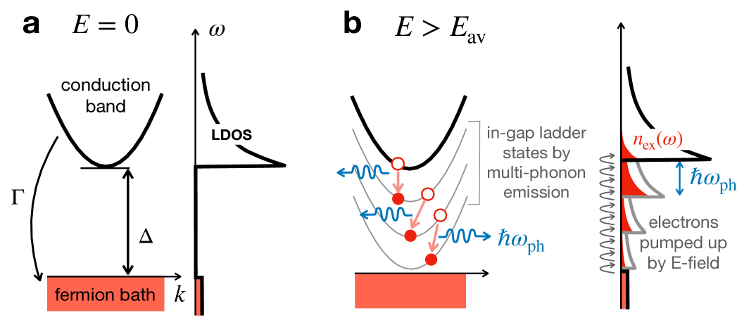
For a conceptual understanding of the avalanche mechanism, we start by considering a one-dimensional conduction band of mass separated by a gap from the Fermi energy, see Fig. 1 a. The electrons are subject to three processes. First, they are accelerated by a DC electric field . Second, they can emit optical phonons of energy by means of an electron-phonon scattering process controlled by the coupling parameter . Finally, dephasing introduces a finite lifetime to the electrons, setting a cutoff on the time scale over which they can form the multi-phonon state. The dephasing may arise from electron tunneling to a substrate, virtual transitions to higher electronic states, and other many-body mechanisms separate from the electron-phonon interaction. Hereafter, we adopt a unit system in which , the electric charge , the Boltzmann constant , and the lattice constant .
Let us now give a back-of-the-envelope criterion for an avalanche that can be triggered by a combination of the three aforementioned electronic processes. We note that, in an insulator subject to an external bias, there will exist dilute, yet nonetheless finite, charge excitations. Due to the Franz-Keldysh effect franzkeldysh , the bandedge smears into the gap and the transition of energetic electrons into those states by phonon emission is substantially enhanced over that in the equilibrium limit. Importantly, electron-phonon scattering processes create a ladder of intermediate replica bands that are equally spaced by . The minimal number of successive phonon-scattering events to bridge the gap is , see Fig. 1b. The timescale it takes to accelerate an electron in a dispersive band, to gain the energy of a single phonon, can be estimated as with the electron band mass . The electron-phonon scattering rate is roughly proportional to the dimensionless electron-phonon mass-renormalization factor , where the typical density of states . The number of phonons that are emitted during the electronic lifetime is then . Consequently, the criterion for the avalanche becomes , yielding the following electric field required to trigger the avalanche
| (2) |
This outcome is highly non-trivial in that the dissipative electron decay rate plays a crucial role in the onset of this nonequilibrium quantum phase transition. The limit is singular in nonequilibrium. By taking before or after the limit, we arrive at an effectively infinite eckstein2011 or a zero temperature (equilibrium) limit, respectively. This singular nature of the limit plays a fundamental role in the avalanche, as will be confirmed below. The switching field is very different in nature from that of Eq. (1), and we note that the avalanche via inelastic scattering is also distinct from the conventional mechanism that has been discussed for high-field transport in semiconductors wolff1954 . Most importantly, as we shall see below, the avalanche fields predicted by Eq. (2) are much smaller than those expected from Eq. (1).
Results
Quantum avalanche in a rigid-band model
To demonstrate the existence of the proposed avalanche mechanism, we
investigate a model of a one-band tight-binding chain under a DC
electric-field , in the Coulomb gauge liprl2015 ; ligraphene
| (3) |
where is the creation/annihilation operator for an electron at site , for which the site position . is the bare gap and is the tight-binding parameter. The electrons are locally coupled to phonons, which are modeled by a collection of harmonic oscillators given by the Hamiltonian
| (4) |
with the amplitude, the momentum, the continuum index, and the frequency of the phonon. In this section we consider the case of optical phonons, with , deferring a discussion of acoustic phonons until later. The on-site electron-phonon coupling is given by
| (5) |
with the coupling constant .
We use the Schwinger-Keldysh formulation of the dynamical mean-field theory (DMFT georges_DMFT1996 ; aoki ; liprl2015 ) which bypasses the transient dynamics and directly yields the homogeneous nonequilibrium steady-state of the many-body dynamics aron2012prl ; prb2013b . The fermion baths enter the computation of the electronic Green’s function via local retarded and lesser self-energies at site as
| (6) |
while the Ohmic baths weiss enter the phonon Green’s function via local self-energies ligraphene ; moire2023 as
| (7) |
In the above expressions, and are the Fermi-Dirac and Bose-Einstein distributions at the bath temperature , respectively, and khurgin2007 is the phonon decay time. We compute the second-order self-energy to electrons and phonons on the same footing. We refer the reader to the Methods Section and to the Supplementary Information for further details on the electron-phonon calculations.
In the calculations that follow, we choose the model parameters , , , , , and in units of eV. We use the lattice constant Å to compute the electric-field. We verify the schematic estimate of the avalanche field, Eq. (2), via systematic comparison with full many-body calculations over a wide range of parameters, as detailed in the Supplementary Information. There, we demonstrate the conceptual validity of the avalanche as arising from a competition between inelastic transport and dephasing and justify the limitations of Eq. (2) in the high-field limit.
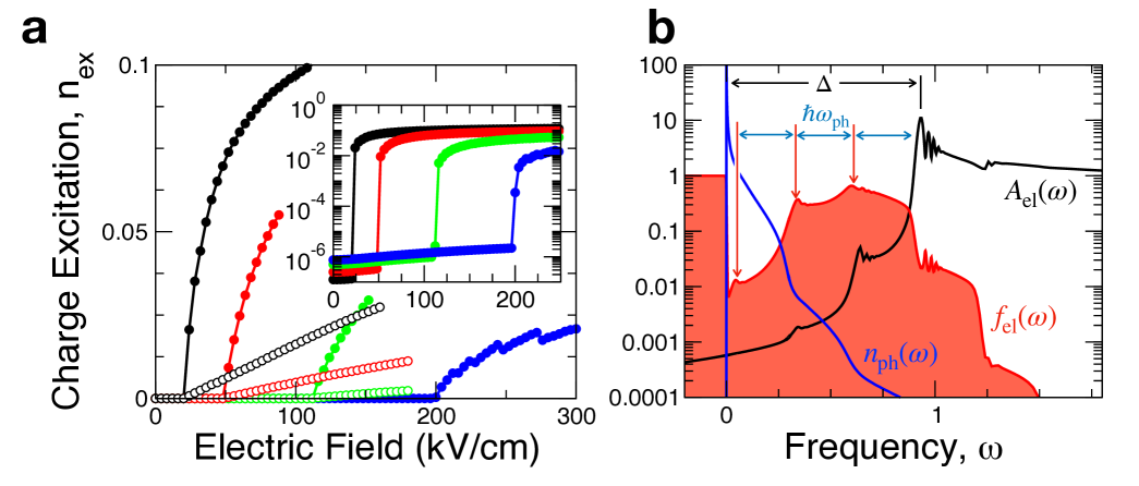
Fig. 2a shows the electronic excitations per site () when ramping up the electric field starting from the insulator state. Filled (empty) symbols denote results obtained by discarding (including) the nonequilibrium self-energy of the phonons. At the onset of the avalanche at the threshold field , increases abruptly, yet continuously, in a similar fashion as in critical phenomena. Notably, is found to be roughly proportional to , consistent with the back-of-the-envelope estimate made in Eq. (2). Furthermore, the pre-avalanche excitations are inversely proportional to [see inset to (a)], which demonstrates that the avalanche is not initiated by thermal excitation but is of quantum origin. Remarkably, the onset of the avalanche is not affected by hot-phonon effects since they are only infinitesimally excited at the continuous avalanche transition, while the incoherence of phonons impedes the avalanche resulting in a linear increase of well after the avalanche.
The nontrivial behavior of the switching field on (see Fig. 2a) should be distinguished from phonon-assisted tunneling kleinman1965 ; vdovin2016 , which is commonly manifested in resonant tunneling in heterostructures. With the electron occupation quickly reaching beyond 0.1 after the avalanche, we are in a metallic bulk limit through a phase transition, instead of in the perturbative tunneling regime. The avalanche shown here only emerges after a fully self-consistent solution is reached after hundreds of iterations, unlike what is expected from a low-order perturbative theory kleinman1965 .
Figure 2b elucidates nature of the nonequilibrium state after the avalanche. The energy distribution reveals a sizable nonequilibrium occupation of the in-gap states around energies at multiples of away from the band edge. This confirms the involvement of multi-phonon emission in the avalanche mechanism. Moreover, the strong deviation of from a Fermi-Dirac distribution points to the non-thermal nature of the avalanche. In contrast, the phonon distribution appears mostly thermal.
Insulator-to-metal transition induced by avalanche
Having established the existence of the avalanche, we now turn our attention to the implications of the avalanche in the context of the resistive transition in correlated insulators. The strong charge fluctuations initiated by the avalanche are expected to generate phonon excitations, which then profoundly perturb the inter-orbital mixing and destabilize the charge gap. To address this point, we extend our model to a two-band correlated insulator where the gap between the bands is generated by electronic interactions. (See Fig. 3a.) Specifically, we consider the following Hamiltonian which allows us to address both the CDW transitions and resistive switching on an equal footing,
| (8) | |||||
Here, is the band index and is the site index on a square lattice with denoting nearest neighbors. The last term in Eq. (8) is the decoupling of an inter-orbital Hubbard-like interaction via an auxiliary quantum field . The magnitude of respresents the order parameter that opens a gap, i.e. the strength of the density modulation in CDW or the charge fluctuations in correlated insulators. The phase of captures the phase slip in CDW materials or the Goldstone excitations in correlated insulators. In this work, we investigate the instability of a uniform symmetry-broken state, and ignore the phase fluctuations of for simplicity. Consideration of -fluctuations would only weaken the order parameter and lead to an even earlier collapse of the insulating state, and thus further supporting our conclusions. The static mean-field condition becomes
| (9) |
The electron-phonon coupling is given by with the independent phonons coupling to each orbital. The fermion/phonon baths are set up as described previously with the Fermi energy at the band crossing.
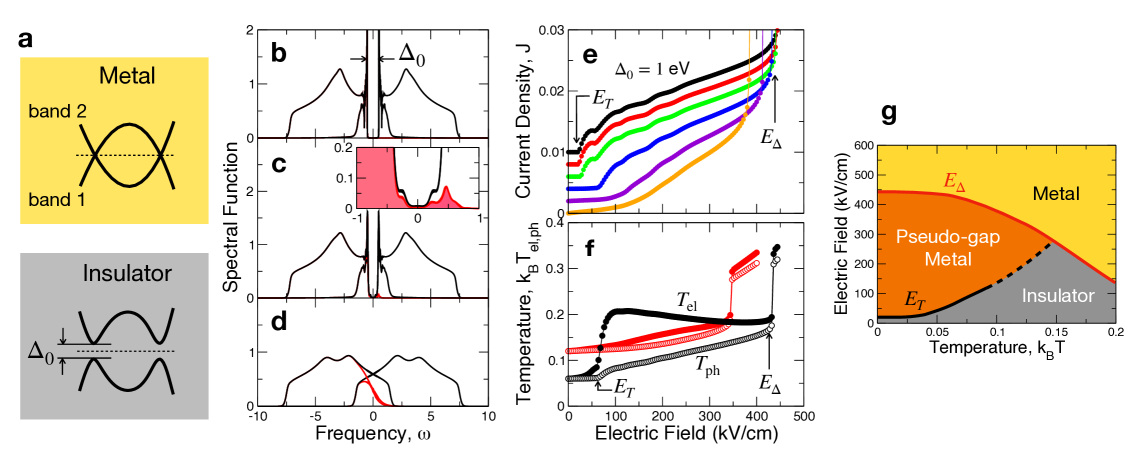
The spectrum of the phonons has important consequences for the IMT. Let us first discuss the electric-field driven IMT in the presence of optical phonons with energy , which we will associate with the multi-stage transitions that are commonly observed in CDW systems. Later, we will turn to the case of acoustic phonons which we will relate to Mott systems. With increasing electric field, the insulating system undergoes a two-stage transition to a metal as manifested by the spectral function in Fig. 3b-d. Here, we adjust the electron-phonon coupling such that, given , the initial gap is tuned to at and at the lowest temperature. The strength of this coupling corresponds to a moderate (dimensionless) mass-renormalization factor of with the phonon energy eV and the 2D density of states . (The damping is set to eV diaz , and the chemical potential to .) In the low-field limit, the spectrum features a well-defined charge gap. As increases beyond the first threshold field , in-gap states develop via the avalanche mechanism. This results in a pseudo-gap phase where the system becomes metallic while the charge gap mostly remains intact. The energy-resolved electron occupation (the red shaded area shown in the inset to panel c) indicates that the electric current is carried mainly by the states of the conduction band above the gap while the in-gap states provide the pathway for this population inversion. The pseudo-gap regime persists until , when the gap collapses to zero in a strongly discontinuous transition.
The current-voltage () relation in Fig. 3e shows evidence of a two-stage IMT. First, the system continuously becomes metallic at the threshold field . Later, at the higher threshold , the current rises discontinuously. The avalanche behavior discussed in Fig. 2 is responsible for the threshold behavior at . This behavior is similar to that in CDW systems, in which it has been widely attributed to the depinning transition fukuyama1978 ; lee1979 . Here, we propose an alternative mechanism of electron avalanche via inelastic scattering that does not require any disorder or reduced dimensionality. With coupling to optical phonons, the avalanche is not sufficiently disruptive to the gap, and the intermediate gapped state is instead sustained over a wide range of electric field (). We note that is around two orders of magnitude smaller than the switching field expected for zero electron-phonon coupling strength MV/cm.
The non-thermal nature of the avalanche transition is illustrated by the electric-field dependence of the effective temperatures for electrons and phonons, as shown in Fig. 3f. (See Methods for the definition of effective temperatures.) As the electric field is increased beyond , the electrons heat up immediately while the phonons stay cold. This clearly demonstrates that heat exchange does not trigger the avalanche. On the other hand, the full IMT at is initiated once the electron and phonon temperatures equilibrate, suggesting that this second transition can be described in terms of a thermal mechanism. It is remarkable to demonstrate that the mechanisms for electronic and thermal switching, the topic of intense discussions in the literature, are not exclusive of each other but can arise simultaneously from a single microscopic model.
The phase diagram defined by the two switching fields ( and ) is plotted in Fig. 3g. The most notable observation here is that remains constant near zero temperature, but increases at higher temperatures until it merges with . This may seem counter-intuitive, since the gap is expected to decrease with increasing . The gap, however, remains nearly constant until close to a critical temperature , meaning that a thermal argument is not applicable. We find that, as suggested by the hot-phonon effects apparent in Fig. 2, thermal decoherence may be detrimental to the avalanche, meaning that a stronger electric field is required to induce an avalanche. This is a further evidence that the threshold behavior is of quantum-mechanical origin. In contrast to , decreases with , and is conventional and thermally driven.
The existence of bias-driven multiple-stage transitions in CDW systems has been intensely debated bardeenPT ; zaitsev-zotov2004 ; zaitsev-zotov2001 ; itkis1990 ; fleming1980 . For instance, recent ARPES studies on the NbSe3 system have shown unambiguously that the various CDW gap energies are constant (marginally increasing) with increasing temperature and observable even beyond their respective values nicholson2017 ; nicholson2020 . This suggests a nonthermal mechanism of gap formation below . At temperatures beyond , the gap gradually closes suggesting a thermal mechanism, where these predictions show an interesting parallel to our results. What our model as a conceptual framework showed are that the nature of the initial threshold itkis1990 in the low field limit is quantum in the sub-gap energy scale, and that, after an intermediate pseudo-gapped phase, there are subsequent discontinuous resistive transitions that thermally destroy the order parameter.
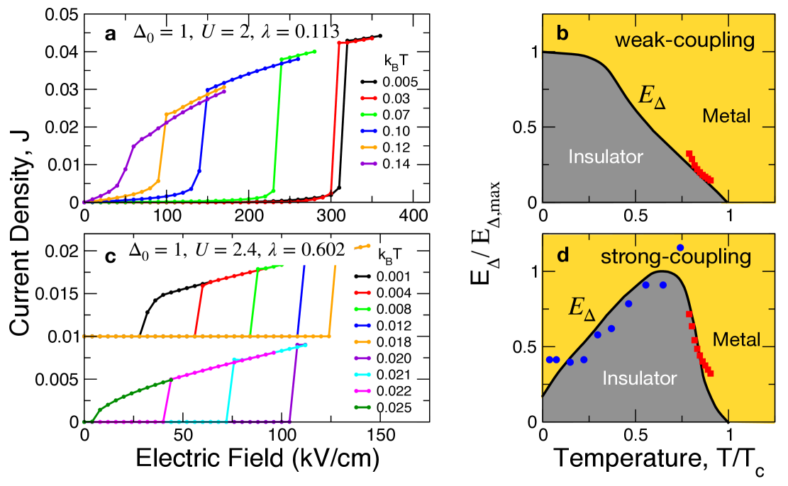
Finally, let us discuss the case of electron coupling to acoustic phonons, with a continuous spectrum of the form and cutoff Debye energy chosen as eV. Compared to optical phonons, the influence of acoustic phonons on the nonequilibrium dynamics is more dramatic. We discuss this situation for both the weak and strong limits of electron-phonon coupling, as shown in Fig. 4. In the weak-coupling limit (), corresponding to panels (a) and (b), the IMT is dominated by a strongly discontinuous collapse of the gap. While the signature of the avalanche is still present as a precursor to the IMT, the range of the avalanche region is much narrower than that found for coupling to optical phonons. The avalanche current is also very small so that its effect is insignificant. decreases monotonically with increasing temperature and the phase diagram is conventional and fully consistent with the thermal switching scenario. We tested this result against experimental data by overlaying the experimental switching fields in the Vanadium oxides WxV1-xO2 tlwu at temperatures close to the transition temperature. In addition to an overall agreement of the trends, the lightly concave curve shape tlwu ; maki1986 found in the experiment is reproduced by the theory.
In the strong electron-phonon coupling limit (), on the other hand, is strongly nonmonotonic, increasing with in the low- limit. As is especially apparent from panel (c), the intermediate field region between and has diminished dramatically so that the IMT appears as a fully single-stage transition, as often observed in correlated transition-metal oxides janod ; stoliar ; zimmers ; guenon ; htkim . In this limit, the strong low-energy excitations of acoustic phonons cause the IMT to bypass the CDW-like pseudo-gap state. We therefore make a prediction that the avalanche physics which controls the CDW threshold field is manifested in Mott insulators in a switching field that increases with . We compare our results with the single-stage switching fields measured in TiS3 randleACSnano ; randleAPL2022 (blue circles). The agreement between theory and experiment is quite reasonable. Altogether, the behavior in the weak- and strong-coupling limits demonstrates a crossover between the quantum and thermal switching mechanisms as temperature is varied.
To conclude, we have established a quantum avalanche mechanism as a generic scenario for the nonequilibrium phase transition in correlated insulators. The proposed mechanism not only resolves the long-standing discrepancy between the observed and predicted switching fields in these materials, but also sheds new light on the origins of the crossover between the quantum and thermal scenarios in resistive transitions. The existence of the pseudo-gapped metallic states may be directly verified experimentally by using transient electrical pulses of varying duration to control the amount of hot-phonon generation. While we have discussed this mechanism with electron-phonon coupling, the avalanche may also arise via coupling to other bosonic excitations, such as the Goldstone modes associated with the order parameter responsible for the opening of the charge gap. Such a scenario may provide a more direct path for the destruction of the correlated gap. Here we have presented a minimal framework for the quantum avalanche that is fundamentally different from the Landau-Zener mechanism. The study of the avalanche with spatial inhomogeneity, and its interplay with disorder, is left for future research.
Methods
Calculation of Self-Energy and Effective Temperature: The many-body calculations in this work are based on the nonequilibrium Green’s function technique approximated by the DMFT scheme aoki ; liprl2015 ; ligraphene ; moire2023 , in which we limit the self-energy to be diagonal in site and orbital indices. Full details on the nonequilibrium DMFT are given in the Supplementary Information. The electron and phonon self-energies, expressed respectively as
| (10) | |||||
| (11) |
are iterated to convergence. (The factor 2 in the phonon self-energy accounts for spin degeneracy.) The self-energies without the vertex correction, i.e., Migdal approximation schrieffer , are reasonable since we are in the weak- to moderate el-ph coupling limit, as can be seen with less than 10% level shift of the bandedge in Fig. 2(b).
Once we achieve full convergence, we compute the distribution functions as
| (12) |
We define the effective temperature for electrons and phonons in terms of the first moment of the distribution, which correctly reduces to the bath temperature in the equilibrium limit, as
| (13) |
with the step-function . As shown in Fig. 2b, electronic distribution functions may deviate strongly from the Fermi-Dirac form, in which cases provides an approximate measure of nonequilibrium energy excitation.
References
- (1) Bardeen, J. Superconductivity and other macroscopic quantum phenomena. Physics Today 25 (1990).
- (2) Bardeen, J. Classical versus quantum models of charge-density-wave depinning in quasi-one-dimensional metals. Phys. Rev. B 39, 3528–3532 (1989). URL https://link.aps.org/doi/10.1103/PhysRevB.39.3528. Publisher: American Physical Society.
- (3) Ong, N. P. et al. Effect of impurities on the anomalous transport properties of NbSe3. Phys. Rev. Lett. 42, 811–814 (1979). URL https://link.aps.org/doi/10.1103/PhysRevLett.42.811.
- (4) Grüner, G. The dynamics of charge-density waves. Rev. Mod. Phys. 60, 1129–1181 (1988). URL https://link.aps.org/doi/10.1103/RevModPhys.60.1129. Publisher: American Physical Society.
- (5) Maki, K. Creation of soliton pairs by electric fields in charge-density-wave condensates. Phys. Rev. Lett. 39, 46–48 (1977). URL https://link.aps.org/doi/10.1103/PhysRevLett.39.46. Publisher: American Physical Society.
- (6) Thorne, R. E. A history of the I-V characteristic of CDW conductors. Journal de Physique IV (Proceedings) 131, 89–94 (2005). URL http://www.edpsciences.org/10.1051/jp4:2005131020.
- (7) Zener, C. Non-adiabatic crossing of energy levels. Proc. R. Soc. A 137, 696–702 (1932).
- (8) Fukuyama, H. & Lee, P. Dynamics of charge-density wave. 1. Impurity pinning in a single chain. Phys. Rev. B 17, 535–541 (1978). URL http://gateway.webofknowledge.com/gateway/Gateway.cgi?GWVersion=2&SrcAuth=mekentosj&SrcApp=Papers&DestLinkType=FullRecord&DestApp=WOS&KeyUT=A1978EN01600017.
- (9) Lee, P. A. & Rice, T. M. Electric field depinning of charge density waves. Phys. Rev. B 19, 3970–3980 (1979). URL https://link.aps.org/doi/10.1103/PhysRevB.19.3970.
- (10) Fisher, D. S. Sliding charge-density waves as a dynamic critical phenomenon. Phys. Rev. B 31, 1396–1427 (1985). URL https://link.aps.org/doi/10.1103/PhysRevB.31.1396.
- (11) Janod, E. et al. Resistive switching in Mott insulators and correlated systems. Adv. Func. Mater. 25, 6287–6305 (2015).
- (12) Stoliar, P. et al. Universal electric-field-driven resistive transition in narrow-gap Mott insulators. Adv. Mater. 25, 3222–3226 (2013).
- (13) Guiot, V. et al. Avalanche breakdown in GaTa4Se8-xTex narrow-gap Mott insulators. Nat. Comm. 4, 1722–6 (2013).
- (14) Ridley, B. K. Specific negative resistance in solids. Proc. Phys. Soc. 82, 954 (1963).
- (15) Lee, S. B. et al. Strong resistance nonlinearity and third harmonic generation in the unipolar resistance switching of NiO thin films. Appl. Phys. Lett. 93, 252102 (2008).
- (16) Zhang, J. et al. Nano-Resolved Current-Induced Insulator-Metal Transition in the Mott Insulator Ca2RuO4. Phys. Rev. X 9, 011032 (2019). URL https://link.aps.org/doi/10.1103/PhysRevX.9.011032.
- (17) del Valle, J., Ramirez, J. G., Rozenberg, M. J. & Schuller, I. K. Challenges in materials and devices for resistive-switching-based neuromorphic computing. J. Appl. Phys. 124, 211101–24 (2018). URL http://aip.scitation.org/doi/10.1063/1.5047800. Publisher: AIP Publishing LLC.
- (18) Oka, T., Arita, R. & Aoki, H. Breakdown of a Mott insulator: A nonadiabatic tunneling mechanism. Phys. Rev. Lett. 91, 66406 (2003).
- (19) Mazza, G., Amaricci, A., Capone, M. & Fabrizio, M. Field-driven Mott gap collapse and resistive switch in correlated insulators. Phys. Rev. Lett. 117, 176401 (2016).
- (20) Sugimoto, N., Onoda, S. & Nagaosa, N. Field-induced metal-insulator transition and switching phenomenon in correlated insulators. Phys. Rev. B 78, 155104 (2008).
- (21) Han, J. E., Li, J., Aron, C. & Kotliar, G. Nonequilibrium mean-field theory of resistive phase transitions. Phys. Rev. B 98, 035145 (2018). URL https://arxiv.org/abs/1804.10733.
- (22) Li, J., Aron, C., Kotliar, G. & Han, J. E. Microscopic theory of resistive switching in ordered insulators: Electronic versus thermal mechanisms. Nano Lett. 17, 2994–2998 (2017). URL http://pubs.acs.org/doi/abs/10.1021/acs.nanolett.7b00286.
- (23) Miller, J., Ordonez, C. & Prodan, E. Time-correlated soliton tunneling in charge and spin density waves. Phys. Rev. Lett. 84, 1555–1558 (2000). URL https://link.aps.org/doi/10.1103/PhysRevLett.84.1555.
- (24) Keldysh, L. V. The effect of a strong electric field on the optical properties of insulating crystals. Sov. Phys. JETP 34, 788 (1958).
- (25) Davies, J. H. & Wilkins, J. W. Narrow electronic bands in high electric fields: Static properties. Physical Review B 38, 1667–1680 (1988). URL https://link.aps.org/doi/10.1103/PhysRevB.38.1667.
- (26) Zhang, S. & Chern, G.-W. Nonequilibrium Dynamics of Gating-Induced Resistance Transition in Charge Density Wave Insulators (2022). URL http://arxiv.org/abs/2201.02194. ArXiv:2201.02194 [cond-mat].
- (27) Zimmers, A. et al. Role of thermal heating on the voltage induced insulator-metal transition in VO2. Phys. Rev. Lett. 110, 056601 (2013).
- (28) Giorgianni, F., Sakai, J. & Lupi, S. Overcoming the thermal regime for the electric-field driven Mott transition in Vanadium Sesquioxide. Nat. Comm. 10, 1–6 (2019). URL http://dx.doi.org/10.1038/s41467-019-09137-6. Publisher: Springer US.
- (29) Jager, M. F. et al. Tracking the insulator-to-metal phase transition in VO2 with few-femtosecond extreme UV transient absorption spectroscopy. Proc. Nat. Aca. Sci. 114, 9558–9563 (2017).
- (30) Kumai, R., Okimoto, Y. & Tokura, Y. Current-induced insulator-metal transition and pattern formation in an organic charge-transfer complex. Science 284, 1645–1647 (1999). URL http://www.sciencemag.org/content/284/5420/1645.short. Publisher: American Association for the Advancement of Science.
- (31) Ribeiro, P., Antipov, A. E. & Rubtsov, A. N. Nonequilibrium breakdown of a correlated insulator through pattern formation. Phys. Rev. B 93, 144305 (2016). URL http://link.aps.org/doi/10.1103/PhysRevB.93.144305.
- (32) Tanaka, Y. & Yonemitsu, K. Crossover from bias-induced to field-induced breakdown in one-dimensional band and Mott insulators attached to electrodes. Phys. Rev. B 83, 085113 (2011). URL https://link.aps.org/doi/10.1103/PhysRevB.83.085113.
- (33) Dutta, A. & Majumdar, P. Spatial behavior in a Mott insulator near the voltage-driven resistive transition. Phys. Rev. B 101, 245155 (2020). URL https://link.aps.org/doi/10.1103/PhysRevB.101.245155.
- (34) Zhu, X., Cao, Y., Zhang, J., Plummer, E. W. & Guo, J. Classification of charge density waves based on their nature. Proceedings of the National Academy of Sciences 112, 2367–2371 (2015). URL http://www.pnas.org/lookup/doi/10.1073/pnas.1424791112.
- (35) Eckstein, M. & Werner, P. Damping of Bloch Oscillations in the Hubbard Model. Phys. Rev. Lett. 107, 186406 (2011).
- (36) Wolff, P. A. Theory of electron multiplication in Silicon and Germanium. Phys. Rev. 95, 1415 (1954).
- (37) Li, J., Camille Aron, Kotliar, G. & Han, J. E. Electric-field-driven resistive switching in the dissipative Hubbard model. Phys. Rev. Lett. 114, 226403 (2015). URL http://journals.aps.org/prl/abstract/10.1103/PhysRevLett.114.226403.
- (38) Li, J. & Han, J. E. Nonequilibrium excitations and transport of Dirac electrons in electric-field-driven graphene. Phys. Rev. B 97, 205412 (2018). URL https://link.aps.org/doi/10.1103/PhysRevB.97.205412. Publisher: American Physical Society.
- (39) Georges, A., Kotliar, G., Krauth, W. & Rozenberg, M. Dynamical mean-field theory of strongly correlated fermion systems and the limit of infinite dimensions. Rev. Mod. Phys. 68, 13–125 (1996).
- (40) Aoki, H. et al. Nonequilibrium dynamical mean-field theory and its applications. Rev. Mod. Phys. 86, 779–837 (2014).
- (41) Aron, C., Kotliar, G. & Weber, C. Dimensional crossover driven by an electric field. Phys. Rev. Lett. 108, 086401 (2012).
- (42) Han, J. E. & Li, J. Energy dissipation in a DC-field-driven electron lattice coupled to fermion baths. Phys. Rev. B 88, 075113 (2013). URL http://link.aps.org/doi/10.1103/PhysRevB.88.075113.
- (43) Weiss, U. Quantum Dissipative Systems (World Scientific, London, 2008).
- (44) Nathawat, J. et al. Signatures of hot carriers and hot phonons in the re-entrant metallic and semiconducting states of Moiré-gapped graphene. Nat. Comm. 14, 1507 (2023). URL https://www.nature.com/articles/s41467-023-37292-4.
- (45) Khurgin, J., Ding, Y. J. & Jena, D. Hot phonon effect on electron velocity saturation in GaN: A second look. Appl. Phys. Lett. 91, 252104–3 (2007). URL http://aip.scitation.org/doi/10.1063/1.2824872.
- (46) Kleinman, L. Theory of phonon-assisted tunneling in semiconductors. Phys. Rev. 140, A637–A648 (1965). URL https://link.aps.org/doi/10.1103/PhysRev.140.A637.
- (47) Vdovin, E. . I. et al. Phonon-assisted resonant tunneling of electrons in graphene-Boron Nitride transistors. Phys. Rev. Lett. 116, 186603 (2016). URL https://link.aps.org/doi/10.1103/PhysRevLett.116.186603.
- (48) Díaz, M. I., Han, J. E. & Aron, C. Electrically-driven insulator-to-metal transition in a correlated insulator: electronic mechanism and thermal description (2022). URL https://arxiv.org/abs/2209.02758.
- (49) Zaitsev-Zotov, S. V. Finite-size effects in quasi-one-dimensional conductors with a charge-density wave. Physics-Uspekhi 47, 533–554 (2004). URL http://stacks.iop.org/1063-7869/47/i=6/a=R01?key=crossref.ac4e2eeb5551029c28c63e82d102319c.
- (50) Zaitsev-Zotov, S. V., Pokrovskii, V. Y. & Monceau, P. Transition to 1D conduction with decreasing thickness of the crystals of TaS3 and NbSe3 quasi-1D conductors. JETP Lett. 73, 25–27 (2001). URL http://link.springer.com/10.1134/1.1355400.
- (51) Itkis, M. E., Nad’, F. Y. & Monceau, P. Nonlinear conductivity of quasi-one-dimensional TaS at low temperatures. J. Phys. Condens. Matter 2, 8327–8335 (1990). URL https://iopscience.iop.org/article/10.1088/0953-8984/2/42/010.
- (52) Fleming, R. M. Electric-field depinning of charge-density waves in NbSe3. Phys. Rev. B 22, 5606–5612 (1980). URL https://link.aps.org/doi/10.1103/PhysRevB.22.5606.
- (53) Nicholson, C. . I. et al. Dimensional crossover in a charge density wave material probed by angle-resolved photoemission spectroscopy. Phys. Rev. Lett. 118, 206401 (2017). URL http://link.aps.org/doi/10.1103/PhysRevLett.118.206401.
- (54) Nicholson, C. W. et al. Role of a higher-dimensional interaction in stabilizing charge density waves in quasi-one-dimensional NbSe3 revealed by angle-resolved photoemission spectroscopy. Phys. Rev. B 101, 045412 (2020). URL https://link.aps.org/doi/10.1103/PhysRevB.101.045412.
- (55) Wu, T.-L., Whittaker, L., Banerjee, S. & Sambandamurthy, G. Temperature and voltage driven tunable metal-insulator transition in individual WxV1-xO2 nanowires. Phys. Rev. B 83, 073101 (2011).
- (56) Randle, M. et al. Gate-controlled metal-insulator transition in TiS3 nanowire field-effect transistors. ACS Nano 13, 803–811 (2018). URL http://pubs.acs.org/doi/10.1021/acsnano.8b08260. Publisher: American Chemical Society.
- (57) Randle, M. D. et al. High-electric-field behavior of the metal-insulator transition in TiS nanowire transistors. Appl. Phys. Lett. 120, 073102 (2022). URL https://aip.scitation.org/doi/10.1063/5.0083166.
- (58) Maki, K. Thermal fluctuations of the order parameter in charge-density waves. Phys. Rev. B 33, 2852–2854 (1986). URL http://gateway.webofknowledge.com/gateway/Gateway.cgi?GWVersion=2&SrcAuth=mekentosj&SrcApp=Papers&DestLinkType=FullRecord&DestApp=WOS&KeyUT=A1986A018700099.
- (59) Guénon, S. et al. Electrical breakdown in a V2O3 device at the insulator-to-metal transition. Europhys. Lett. 101, 57003 (2013).
- (60) Kim, H.-T. et al. Electrical oscillations induced by the metal-insulator transition in VO2. J. Appl. Phys. 107, 023702 (2010).
- (61) Schrieffer, J. R. Theory of Superconductivity (Addison Wesley, New York, 1994).
Acknowledgements
JEH is grateful for computational support from the CCR at Buffalo. JEH is supported by Air Force Office of Scientific Research under award no. FA9550-22-1-0349. CA acknowledges the support from the French ANR “MoMA” project ANR-19-CE30-0020 and from the project 6004-1 of the Indo-French Centre for the Promotion of Advanced Research (IFCPAR). JHH acknowledges the support from the Institute for Basic Science in the Republic of Korea through the project IBS-R024-D1. KSK was supported by the Ministry of Education, Science, and Technology (Grants No. NRF-2021R1A2C1006453 and No. NRF-2021R1A4A3029839) of the National Research Foundation of Korea (NRF) and by TJ Park Science Fellowship of the POSCO TJ Park Foundation. We are much grateful to Sambandamurthy Ganapathy, Han-Woong Yeom, Emmanuel Baudin for helpful discussions.