New spin-polarized electron source based on alkali-antimonide photocathode
Abstract
New spin-dependent photoemission properties of alkali antimonide semiconductor cathodes are predicted based on the detected optical spin orientation effect and DFT band structure calculations. Using these results, the Na2KSb/Cs3Sb heterostructure is designed as a spin-polarized electron source in combination with the Al0.11Ga0.89As target as a spin-detector with spatial resolution. In the Na2KSb/Cs3Sb photocathode, spin-dependent photoemission properties were established through detection of high degree of photoluminescence polarization and high polarization of the photoemitted electrons. It was found that the multi-alkali photocathode can provide electron beams with emittance very close to the limits imposed by the electron thermal energy. The vacuum tablet-type sources of spin-polarized electrons have been proposed for accelerators, that can exclude the construction of the photocathode growth chambers for photoinjectors.
In recent decades, the physics of spin-polarized electrons in semiconductors has proven to be not only a fascinating area of basic research, but also a fruitful field of device applications that have had a significant impact on several areas of modern physics. Spin-polarized electron beams with high currents are required by modern and future nuclear physics facilities such as the Electron Ion Collider (EIC), the International Linear Collider [1, 2, 3, 4, 5] and for developing new generation of electron-positron collider ”Super charm-tau factory” [6] with a variety of uses.
Long lifetime polarized electron sources are also of interest for electron microscopy methods exploiting spin polarization to probe magnetization in materials and nanostructures [7, 8]. Probing the spin-resolved electron states of solids, surfaces and nanostructures give direct access to phenomena like magnetism [9], proximity effects [10], spin–orbit interaction [11] and related spin texture in low-dimensional systems [12], which are regarded as potential functional systems for developing low-energy fast spintronic sensors or logic devices.
Almost all modern electron sources for highly spin-polarized electron beams in accelerator physics and electron microscopy rely on photocathode materials based on III-V (GaAs) technology. The first realization of a GaAs spin-polarized source was made by Pierce et. al. [13] in 1975 based on both the phenomenon of optical orientation of electron spins in semiconductors (creation of spin-oriented carriers with absorption of circularly polarized light) and the discovery of negative electron affinity (NEA) activation of -type semiconductor surfaces. The appearance of charge carriers with oriented spins upon absorption of a circularly polarized light was originally studied by Garvin et al. [14] and by Lampel and Weibush [15]. Despite the widespread use of GaAs as a photocathode, a serious disadvantage of the GaAs cathode is its sensitivity to residual vacuum gases and, as a consequence, a short lifetime (or very low quantum efficiency) [16]. A more stable semiconductor electron emitter sources are based on the alkali metal antimonide cathodes [4].
Alkali antimonide semiconducting materials are of great interest for single photon detection in photomultiplier devices [17, 18, 19] and as electron sources for the generation of high brightness electron beams for the next generation light sources like Energy Recovery Linacs (ERL’s) and Free Electron Lasers [20, 3, 21]. The advantage of these photocathodes is provided by their faster temporal response compared to III-V photoemitters. It was also demonstrated that the multi-alkali photocathode can provide bright electron beams with intrinsic emittance very close to the limits imposed by the electron thermal energy (0.22 mm-mrad/(mm rms) corresponding to a Mean Transverse Energy (MTE) of 30 meV at room temperature) [22]. The epitaxial growth of thin films of the high-efficiency photocathode alkali antimonide materials by molecular-beam epitaxy opens the way to a significant increase in brightness and efficiency near the threshold by reducing surface disorder [23, 24, 25]. All this leads to the fact that some groups switch from GaAs photocathode to alkaline antimony photocathode for DC gun or RF gun [1].
First attempts to use photosensitive materials, such as Cs3Sb, K2CsSb, Na2KSb, and Na2KSb:Cs for electron sources have been performed since the 1930s [26, 27, 28], however, surprisingly, the possibility of their use as a source of spin-polarized electrons has not been studied so far.
This Letter presents the first observation of spin-polarized photoemission from alkali-antimonide semiconductor heterostructures. The vacuum spin-photodiode consisting of semiconductor Na2KSb photocathode and Al0.11Ga0.89As spin-detector, both activated to NEA states, is implemented and high spin polarization of photoemitted electrons from Na2KSb measured in spectral and image modes is demonstrated.
From a technological point of view, knowledge of the electronic structure and spin texture is essential in order to understand the spin-polarized photoemission properties.
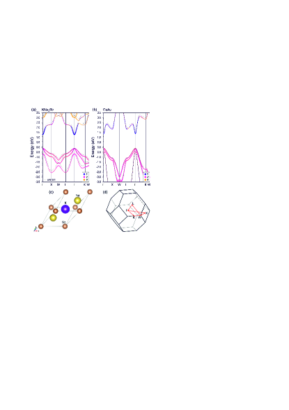
The calculated dispersion of the electron bands of cubic Na2KSb is shown in Fig. 1(a). In the density functional theory (DFT) calculations performed with the Vienna Ab Initio Simulation Package (VASP) [29, 30], where the generalized gradient approximation (GGA-PBE) [31] for the exchange-correlation potential was applied and the interaction between the ion cores and valence electrons was described by the projector augmented-wave method [32, 33], the alkali metals orbitals were treated as valence electrons. To obtain realistic bulk gap the Slater-type DFT-1/2 self-energy correction method [34, 35] with a partially (quaternary) ionized antimony potential was applied.
At the first glance, one can see a very similar band structure for Na2KSb and GaAs (calculated within similar approach, Fig. 1(b)). Gray lines in Fig. 1 show the spectra calculated with switched-off spin-orbit interaction (SOI) for both Na2KSb and GaAs, where three topmost valence bands are degenerate at and the band gaps are 1.58 and 1.62 eV, respectively. The calculated energy band dispersion of the non-relativistic electronic structure of Na2KSb and symmetries of the bands in the center of the Brillouin zone agree well with the earlier calculations performed within the localized spherical wave method [36] with the exception of smaller band gap in the latter case (0.9 eV), as well as with results obtained within approximation (1.51 eV) [37] with which there is a fine agreement. Switching SOI on leads to a slight narrowing of the band gaps, to 1.41 and 1.51 eV, respectively. However, the main changes occur in the valence band, that is by 90% is determined by the states of Sb(As). The heavy-hole and light-hole valence bands remain degenerate while the third band splits off. This splitting is about twice larger in Na2KSb (0.55 eV vs. 0.34 eV in GaAs). These bands form initial states in the photoabsorption process.
Thus, the similarity of the band structures of the Na2KSb and GaAs allows us to conclude that the optical orientation of electron spins is possible in the Na2KSb, and, consequently, the photoemission of spin-polarized electrons.
.
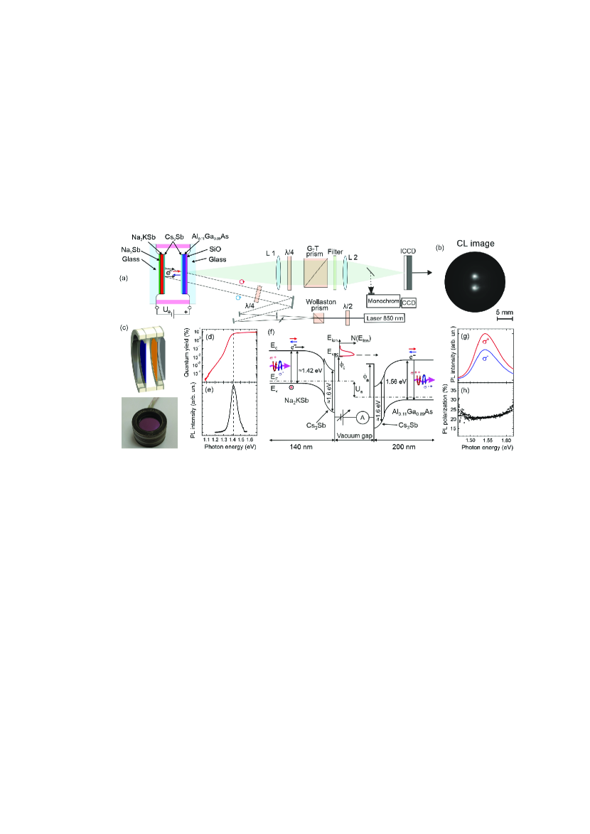
In our previous work [38] we developed an image-type spin detector prototype for measuring the normal (to the surface of the detector) component of the electron beam polarization. This detector is based on the injection of spin-polarized free electrons from GaAs/(CsO) cathode into a heterostructure with GaAs/AlxGa1-xAs quantum wells (QWs) and recording the circularly polarized cathodoluminescence (CL) with spatial resolution. A flat vacuum photodiode composed of two effective NEA semiconductor electrodes was designed and studied in Refs. [39, 40, 41, 42]. In this work we demonstrate that alkali antimonide photocathode can be utilized as an effective source of spin-polarized electrons and the anode - Al0.11Ga0.89As/Cs3Sb heterostructure, as the spin detector. Schematic presentation of the compact vacuum photodiode with a photo of the device and investigation of spin-dependent injection are shown in Fig. 2(a). The photocathode consists of an active 140 nm Na2KSb layer grown on the glass of the input window and activated to NEA by Cs3Sb layer. The semiconductor anode (target) comprises 200 nm Al0.11Ga0.89As layer with SiO coating, through which the structure is bonded to the glass of the output window. The final step of the cleaning procedure for the anode was carried out inside a glove box flooded with pure nitrogen, in which the anode was chemically treated in a solution of HCl in isopropanol [43]. The cleaned Al0.11Ga0.89As anode surface was also activated to the NEA state by coadsorption of cesium and antimony. Similar activation layer was utilized earlier for GaAs [44]. The photocathode and anode were plane-parallel mounted in an air-tight manner on the opposite flat sides of a cylindrical alumina ceramics body. The diameters of the cathode and anode were 18 mm with a 1.0 mm gap between the electrodes. To compare spin-dependent photoemission properties of Na2KSb/Cs3Sb photocathode with the GaAs one, we also constructed and studied the vacuum spin-photodiode with GaAs/(Cs,O) cathode and the same Al0.11Ga0.89As/(Cs,O) anode. Based on the developed vacuum diode (Fig. 2(c)), the tablet-type sources of spin-polarized electrons can be manufactured and used for accelerators. The evacuated photocathode source can be opened in the photoinjector, thus potentially eliminating the construction of photocathode growth chambers (see Supplemental Material, Fig. S1 [45]).
Quantum yield (QY) of Na2KSb photocathode measured in the transmission mode as a function of the incident photon energy in combination with photoluminescence spectrum are shown in Fig. 2(d). The QY is calculated as the ratio of the registered electrons per incident photons. The quantum yield has the threshold at about 1.4 eV and increases slightly in the range 1.4-2.5 eV reaching QY maximum at about 15 %. The photoluminescence (PL) spectrum of the Na2KSb photocathode recorded at a room temperature (Fig. 2(e)) shows a peak with the energy of 1.42 eV (887 nm) which corresponds to the Na2KSb optical band gap transition in agreement with DFT calculation (Fig. 1 (a)). One can see that PL peak position coincides well with the photoemission threshold of QY spectra, meaning that the red edge in photoemission spectrum is determined by the energy gap rather than the work function of Na2KSb/Cs3Sb. Thus, the deposition of Cs3Sb layer on Na2KSb leads to formation of the NEA state as follows from QY, PL (Fig. 2(̃d, e)) and energy distribution curves (EDC) measurements (Fig. 5). These results, together with earlier data on Cs3Sb photoemission properties [28], allow us to plot the band diagram shown in (Fig. 2(f)).
To characterize the Al0.11Ga0.89As/Cs3Sb target as a spin-detector first we measured the circularly polarized PL and determined the spectral dependence of the degree of circular polarization of PL (Fig. 2(g)). For -Al0.11Ga0.89As layer of 200 nm thickness under excitation with photon energy = 1.67 eV the degree of PL polarization is about 22 % that is close to the potentially feasible value of 25%. The results of polarized PL measurements show that -Al0.11Ga0.89As can be used for spin polarimetry applications based on the optical detection of the free-electron spin polarization similar to QWs structure used in Ref. [41].
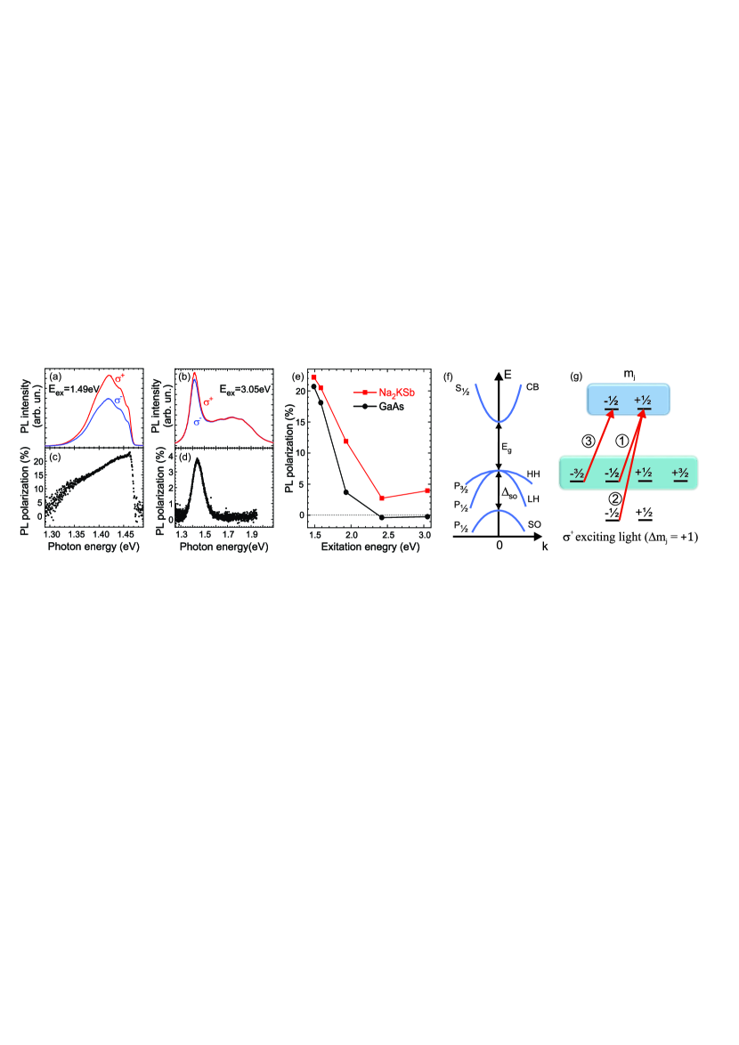
In order to test the polarization properties of the Na2KSb/Cs3Sb photocathode, we measured circularly polarized spectra (, ) of photoluminescence in the optical orientation mode. The polarized PL excited with the circular polarized emission of laser diodes with photon energy = 1.49 eV (850 nm) and = 3.05 eV (405 nm) is shown in Fig. 3 (a) and (b), respectively. The corresponding spectral dependence of the circular polarization degree for the PL emission is shown in the bottom panels in Fig. 3 (c,d). As can be seen, even at excitation energy of 3.05 eV the PL polarization is not zero (4 %). Note that the broad unpolarized peak centered at 1.8 eV in Fig. 3 (b) corresponds to the glass PL emission [46]. Dependence of the PL circular polarization degree on the excitation photon energy in Na2KSb in comparison with GaAs is shown in Fig. 3 (e). At photon energy = 1.49 eV the PL polarization showing a maximum, 23 %, decreases rapidly with rising in the excitation energy up to 2.4 eV. However, in contrast to GaAs, where PL polarization becomes zero, in Na2KSb it remains about 4 % at higher photon excitation energies. Similarity in the polarization dependence of the PL at low excitation energies and in the band structures of Na2KSb and GaAs (Fig. 1 (a,b)) suggests that the optical selection rules for these two semiconductors are the same. Schematic band structure of Na2KSb in the vicinity of the BZ center as derived from the DFT spectrum (Fig. 1(a)) is shown in Fig. 3(f). The conduction band is two-fold degenerate and consists of -like states (total angular momentum ). The valence bands, on the other hand, consist of -like states with a two-fold degenerate heavy-hole and light-hole subband (), and a two-fold degenerate split-off (SO) band () separated by the spin-orbit energy eV in accordance with DFT results. The Fig. 3 (g) shows the optical transitions in Na2KSb between the valence band and the conduction band. The circled numbers indicate the corresponding transition probabilities for right circularly polarized light (). For photons with the energy between and only transitions from the heavy-hole and light-hole states into the conduction band are allowed. These transitions obey selection rules that preserve the angular momentum of the absorbed photon of +1 (or -1 for left polarized light). Thus, circularly polarized light can be used to create an unequal occupation of electrons in Na2KSb with the spin orientation parallel and anti-parallel to the propagation direction of the incident light. If the electrons escape from the multi-alkali photocathode Na2KSb/Cs3Sb into the vacuum, as shown in the band diagram in Fig. 2 (f), we can expect photoemission of spin-polarized electrons.
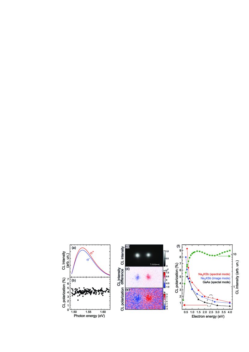
In order to test the Na2KSb/Cs3Sb photocathode as a source of spin-polarized electrons, the injection of photoemitted electrons into the Al0.11Ga0.89As/Cs3Sb heterostructure was studied using spin-polarized cathodoluminescence. Earlier it was shown that semiconductor heterostructures based on III-V compounds can be used as spin detectors of free electrons with spectral and spatial resolution [47, 48, 49, 41, 38]. The polarized CL spectra measured under injection of spin-polarized electrons with the energy of 1.0 eV are shown in Fig. 4 (a). The maximum CL intensity corresponds to the radiation emission energy of 1.53 eV (810 nm), coinciding with the PL maximum of Al0.11Ga0.89As (Fig. 2 (g)). The degree of spectral circular polarization of the CL emission excited by the electrons with the energy of 1.0 eV is equal to 4.5 % (Fig. 4(b)).
Recently we demonstrated that semiconductor spin-detector allows to measure polarization with spatial resolution in direct image mode [38]. Fig. 4 (c) shows the image of spin-integrated CL intensity from two spots induced by two opposite spin-polarized electron beams injected into the Al0.11Ga0.89As/Cs3Sb target (Fig. 2 (a,b)). The image is taken at an accelerating voltage of 1 V and reflects the electron distribution in the cross section. In this case, the CL polarization in the cross section of two electron beams should have the opposite sign and be determined by the polarization of photoemitted electrons exited by absorbed circularly polarized light in the photocathode. Fig. 4 (d) shows the CL intensity difference (). Due to the injection of opposite polarized electron beams and its recombination in Al0.11Ga0.89As, the emitted CL contains both polarized emission components (, ) with helicity oppositely distributed intensity in the two spots (Fig. 4 (d)): spin-up and spin-down . The CL polarization asymmetry image is shown in Fig. 4(e). The detected at electron injection with energy of 1 eV is 3 % (Fig. 4 (e)). The dependences of the CL circular polarization degree determined from spectral and spatial distribution on the injected electron energy in the range of 0.6-4 eV are shown in Fig. 4(f). is maximal, of 9.5 %, at low kinetic energies (0.6 eV) and monotonically decreases down to % as the electron energy increases to 4 eV. Comparing the CL polarization for Na2KSb/Cs3Sb to GaAs photocathode (Fig. 4(f)) one can conclude that the latter is twice less. Assuming that the polarization of photoelectrons from GaAs cathode is in the range of 20-25 % [41], we can conclude that the polarization of photoemitted electrons from Na2KSb/Cs3Sb is in the range of 40-50 %.
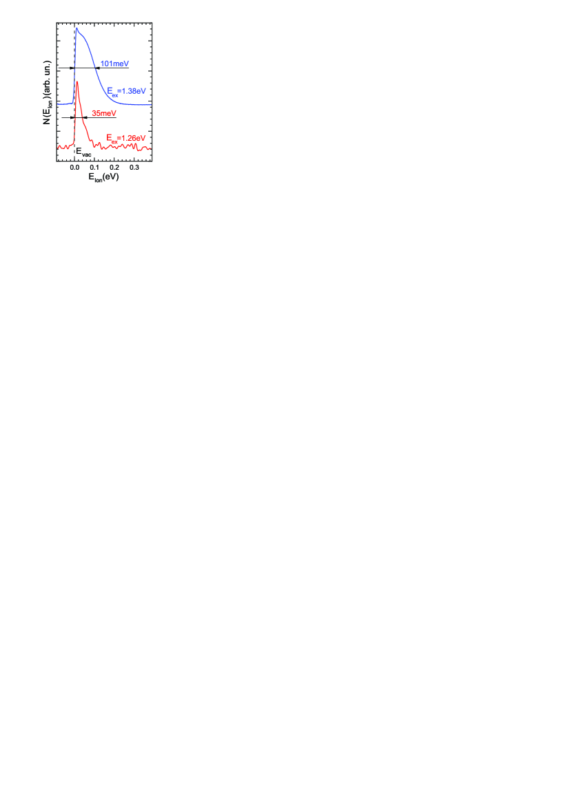
Photoinjectors equipped with low intrinsic emittance photocathodes are among the brightest electron sources in use today [50, 4]. One of the limitations of the peak brightness at the source is the photocathode’s transverse momentum spread. To study the electron emission process via the electron energy distribution, the photoelectron spectra are measured by differentiating the delay curves using the lock-in technique. This allows measuring photoelectron longitudinal (along the beam) energy distributions () by means of the photodiode as a retarding field electron spectrometer [51, 39]. The electron energy distribution curves (EDCs) measured at room temperature for the Na2KSb/Cs3Sb transmission-mode with 1.38 and 1.26 eV photon energies have the widths of 101 and 35 meV, respectively (Fig. 5). The EDC width for photon excitation of 1.38 eV reflects the presence of NEA on the surface with a value of about 100 meV (Fig. 2 (f)). Rapid drop of EDC width to 35 meV with decreasing photon energy proves that the multi-alkali photocathode can provide spin-polarized electron beams with emittance very close to the limits imposed by the electron thermal energy (see Supplemental Material, Fig. S2 [45]). Moreover, the QY at 1.26 eV photon energy is equal to 0.03 % (Fig. 2 (d)) that is much higher than in metallic photocatodes [52].
To summarize, the Na2KSb band structure was found to be very similar to GaAs with the same optical transition rules. However, the SOI gap in the VB of Na2KSb is almost twice larger than that in GaAs. Spin-polarized electrons in the Na2KSb photocathode were obtained by optical pumping with circularly polarized light and showed 23 % polarization of photoluminescence and 40-50 % spin polarization of the emitted electrons. The measured energy spreads of electron beams generated with light having energy lower than 1.3 eV (wavelength longer than 900 nm) are approaching the limit imposed by the thermal energy of electrons at room temperature with quantum efficiencies higher than metallic photocathodes. The AlxGa1-xAs structure has also been shown to be promising as a spatially resolved spin detector for free electrons. High quantum efficiency and low emittance of spin-polarized electron beams provided by multi-alkali photocathodes make them of great interest for next generation high brightness photoinjectors. Finally, based on the created vacuum photodiode, the tablet-type sources of spin-polarized electrons can be manufactured and used for accelerators without construction of the photocathode growth chambers for photoinjectors.
I Supplemental Material
I.1 The tablet-type source of spin-polarized electrons
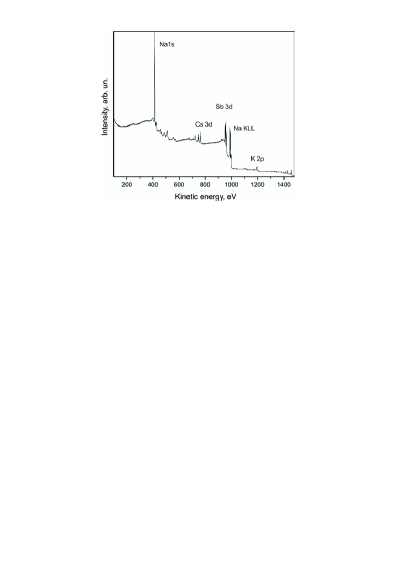
The multialkali photocathodes, owing to their alkali metal content, are extremely sensitive to vacuum contamination and cannot be characterized ex situ. To measure the composition of the cathode surface, a vacuum-sealed diode was opened in an analytical XPS setup. Fig. 6 shows the X-ray photoemission spectrum of the multialkali Na2KSb/Cs3Sb photocathode source after opening the vacuumed photodiode under vacuum condition in the preparation chamber of electron spectrometer. The ratio of alkali components Na:K:Cs and Sb confirms the formation of Na2KSb/Cs3Sb interface.
Based on the vacuum opening technology, the tablet-type sources of spin-polarized electrons can be manufactured separately and used for accelerators.
I.2 Mean transverse energy and emittance
To estimate the mean transverse energy (MTE) of the electrons emitted from the multialkali photocathode the transverse energy distribution curves (TEDC) were studied. For the experiment we used the vacuum photodiode described in polarized cathodoluminescence study. The photocathode was illuminated with 1.26 eV tightly focused laser beam, and its electron emission footprint (cathodoluminescence (CL) image from the anode) was recorded with CCD camera (Fig. 7 (a)). The emission source size was received from the photoluminescence (PL) image recorded from the photocathode. The images of electron emission footprint and emission source were converted to radial profiles for further calculations (Fig. 7 (b)). Since the electron emission footprint is 10 times larger than emission source (Fig. 7 (a, b)) ( 200 m vs 20 m) we consider that the photoelectrons are emitted from a point source. Knowing the distance travelled by the photoelectrons (vacuum gap width) and the voltage through which they have been accelerated (defining their time-of-flight), the transverse energy required to generate the observed emission footprint can be determined:
| (1) |
where , – acceleration, – vacuum gap width (1.55 mm), – acceleration voltage, – electron charge, – electron mass, – distance from the center of the electron emission footprint. Since , longitudinal energy component is neglected. Radial profiles of electrons were transformed to TEDC (Fig. 7 (c)) using the equation:
| (2) |
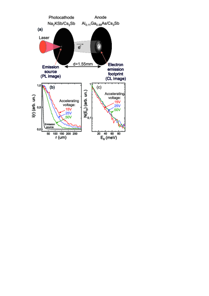
From the fact that TEDC recorded at different acceleration voltages (15, 25, 50 V) are similar one can conclude that electric field is uniform and there is no space charge in the vacuum gap of the photodiode during the experiment. The next step was to calculate the mean transverse energy (MTE) of the electrons emitted from the photocathode. By definition, MTE is given by:
| (3) |
The MTE obtained from the TEDC turned out to be close to the limits imposed by the electron thermal energy (MTE 35 meV). Another parameter used for electron source characterization is the intrinsic emittance . It can be calculated from the MTE as:
| (4) |
where – electron mass, – speed of light. The intrinsic emittance corresponding to the MTE measured equals to 0.26 mmmrad/mm. The values of MTE and are close to the results obtained in other works on multialkali photocathodes [53, 22].
References
- Wang and Aulenbacher [2018] E. Wang and K. Aulenbacher, ERL17 Workshop, WG1 Summary: Injectors, in Proc. 59th ICFA Advanced Beam Dynamics Workshop (ERL’17), Geneva, Switzerland, 2017 (JACoW Publishing, Geneva, Switzerland, 2018) pp. 77–78.
- Aprahamian et al. [2015] A. Aprahamian et al., Reaching for the horizon: The 2015 long range plan for nuclear science, United States (2015).
- Michizono [2019] S. Michizono, The international linear collider, Nature Reviews Physics 1, 244 (2019).
- Musumeci et al. [2018] P. Musumeci, J. Giner Navarro, J. B. Rosenzweig, L. Cultrera, I. Bazarov, J. Maxson, S. Karkare, and H. Padmore, Advances in bright electron sources, Nuclear Instruments and Methods in Physics Research Section A: Accelerators, Spectrometers, Detectors and Associated Equipment 907, 209 (2018).
- Pellegrini [2012] C. Pellegrini, The history of x-ray free-electron lasers, The European Physical Journal H 37, 659 (2012).
- Piminov [2018] P. Piminov, Project for a Super Charm–Tau Factory at BINP, Physics of Particles and Nuclei Letters 15, 732 (2018).
- Suzuki et al. [2010] M. Suzuki, M. Hashimoto, T. Yasue, T. Koshikawa, Y. Nakagawa, T. Konomi, A. Mano, N. Yamamoto, M. Kuwahara, M. Yamamoto, S. Okumi, T. Nakanishi, X. Jin, T. Ujihara, Y. Takeda, T. Kohashi, T. Ohshima, T. Saka, T. Kato, and H. Horinaka, Real time magnetic imaging by spin-polarized low energy electron microscopy with highly spin-polarized and high brightness electron gun, Applied Physics Express 3, 026601 (2010).
- Liang et al. [2018] J. Liang, L. Zhu, and L. V. Wang, Single-shot real-time femtosecond imaging of temporal focusing, Light: Science & Applications 7, 42 (2018).
- Vollmer et al. [2003] R. Vollmer, M. Etzkorn, P. S. A. Kumar, H. Ibach, and J. Kirschner, Spin-polarized electron energy loss spectroscopy of high energy, large wave vector spin waves in ultrathin fcc co films on cu(001), Phys. Rev. Lett. 91, 147201 (2003).
- Buzdin [2005] A. I. Buzdin, Proximity effects in superconductor-ferromagnet heterostructures, Rev. Mod. Phys. 77, 935 (2005).
- Bentmann et al. [2021] H. Bentmann, H. Maaß, J. Braun, C. Seibel, K. A. Kokh, O. E. Tereshchenko, S. Schreyeck, K. Brunner, L. W. Molenkamp, K. Miyamoto, M. Arita, K. Shimada, T. Okuda, J. Kirschner, C. Tusche, H. Ebert, J. Minár, and F. Reinert, Profiling spin and orbital texture of a topological insulator in full momentum space, Phys. Rev. B 103, L161107 (2021).
- Maaß et al. [2016] H. Maaß, H. Bentmann, C. Seibel, C. Tusche, S. V. Eremeev, T. R. F. Peixoto, O. E. Tereshchenko, K. A. Kokh, E. V. Chulkov, J. Kirschner, and F. Reinert, Spin-texture inversion in the giant Rashba semiconductor BiTeI, Nature Communications 7, 11621 (2016).
- Pierce et al. [1975] D. T. Pierce, F. Meier, and P. Zürcher, Direct observation of spin dependent electronic structure of GaAs using spin polarized photoemission, Physics Letters A 51, 465 (1975).
- Garvin et al. [1974] E. L. Garvin, D. T. Pierce, and H. C. Siegmann, Polarized photoelectrons from optically magnetized semiconductors, Helvetica Physica Acta 74, 393 (1974).
- Lampel and Weisbuch [1975] G. Lampel and C. Weisbuch, Proposal for an efficient source of polarized photoelectrons from semiconductors, Solid State Communications 16, 877 (1975).
- Friederich et al. [2019] S. Friederich, K. Aulenbacher, and C. Matejcek, Vacuum Lifetime and Surface Charge Limit Investigations Concerning High Intensity Spin-polarized Photoinjectors, in Proc. 10th International Particle Accelerator Conference (IPAC’19), Melbourne, Australia, 2019, 10 (JACoW Publishing, Geneva, Switzerland, 2019) pp. 1954–1957.
- Bergevin [2015] M. Bergevin, Future water Cherenkov detectors, AIP Conference Proceedings 1663, 100002 (2015).
- Wright [2017] A. Wright, The Photomultiplier Handbook. (Oxford University Press, 2017).
- Lyashenko et al. [2020] A. V. Lyashenko, B. W. Adams, M. Aviles, T. Cremer, C. D. Ertley, M. R. Foley, M. J. Minot, M. A. Popecki, M. E. Stochaj, W. A. Worstell, J. W. Elam, A. U. Mane, O. H. W. Siegmund, H. J. Frisch, A. L. Elagin, E. Angelico, and E. Spieglan, Performance of Large Area Picosecond Photo-Detectors (LAPPDTM), Nuclear Instruments and Methods in Physics Research Section A: Accelerators, Spectrometers, Detectors and Associated Equipment 958, 162834 (2020).
- Dowell et al. [2010] D. H. Dowell, I. Bazarov, B. Dunham, K. Harkay, C. Hernandez-Garcia, R. Legg, H. Padmore, T. Rao, J. Smedley, and W. Wan, Cathode R&D for future light sources, Nuclear Instruments and Methods in Physics Research Section A: Accelerators, Spectrometers, Detectors and Associated Equipment 622, 685 (2010).
- Scholz [2018] M. Scholz, FEL Performance Achieved at European XFEL, in Proc. 9th International Particle Accelerator Conference (IPAC’18), Vancouver, BC, Canada, 2018 (JACoW Publishing, Geneva, Switzerland, 2018) pp. 29–33.
- Cultrera et al. [2016] L. Cultrera, C. Gulliford, A. Bartnik, H. Lee, and I. Bazarov, Ultra low emittance electron beams from multi-alkali antimonide photocathode operated with infrared light, Applied Physics Letters 108, 134105 (2016).
- Yamaguchi et al. [2017] H. Yamaguchi, F. Liu, J. N. Defazio, C. W. N. Villarrubia, D. Finkenstadt, A. Shabaev, K. Jensen, V. Pavlenko, M. J. Mehl, S. G. Lambrakos, G. Gupta, A. D. Mohite, and N. A. Moody, Active bialkali photocathodes on free-standing graphene substrates, npj 2D Materials and Applications 1, 1 (2017).
- Feng et al. [2017] J. Feng, S. Karkare, J. Nasiatka, S. Schubert, J. Smedley, and H. Padmore, Near atomically smooth alkali antimonide photocathode thin films, Journal of Applied Physics 121, 044904 (2017).
- Parzyck et al. [2022] C. T. Parzyck, A. Galdi, J. K. Nangoi, W. J. I. DeBenedetti, J. Balajka, B. D. Faeth, H. Paik, C. Hu, T. A. Arias, M. A. Hines, D. G. Schlom, K. M. Shen, and J. M. Maxson, Single-crystal alkali antimonide photocathodes: High efficiency in the ultrathin limit, Phys. Rev. Lett. 128, 114801 (2022).
- Görlich [1936] P. R. Görlich, Über zusammengesetzte, durchsichtige photokathoden, Zeitschrift für Physik 101, 335 (1936).
- Sommer [1955] A. H. Sommer, New photoemissive cathodes of high sensitivity, Review of Scientific Instruments 26, 725 (1955).
- Spicer [1958] W. E. Spicer, Photoemissive, photoconductive, and optical absorption studies of alkali-antimony compounds, Physical Review 112, 114 (1958).
- Kresse and Hafner [1993] G. Kresse and J. Hafner, Ab initio molecular dynamics for open-shell transition metals, Phys. Rev. B 48, 13115 (1993).
- Kresse and Furthmüller [1996] G. Kresse and J. Furthmüller, Efficient iterative schemes for ab initio total-energy calculations using a plane-wave basis set, Phys. Rev. B 54, 11169 (1996).
- Perdew et al. [1996] J. P. Perdew, K. Burke, and M. Ernzerhof, Generalized gradient approximation made simple, Phys. Rev. Lett. 77, 3865 (1996).
- Blöchl [1994] P. E. Blöchl, Projector augmented-wave method, Phys. Rev. B 50, 17953 (1994).
- Kresse and Joubert [1999] G. Kresse and D. Joubert, From ultrasoft pseudopotentials to the projector augmented-wave method, Phys. Rev. B 59, 1758 (1999).
- Ferreira et al. [2008] L. G. Ferreira, M. Marques, and L. K. Teles, Approximation to density functional theory for the calculation of band gaps of semiconductors, Phys. Rev. B 78, 125116 (2008).
- Ferreira et al. [2011] L. G. Ferreira, M. Marques, and L. K. Teles, Slater half-occupation technique revisited: the LDA-1/2 and GGA-1/2 approaches for atomic ionization energies and band gaps in semiconductors, AIP Advances 1, 032119 (2011).
- Ettema and de Groot [2000] A. R. H. F. Ettema and R. A. de Groot, Electronic structure of Na3Sb and Na2KSb, Phys. Rev. B 61, 10035 (2000).
- Amador et al. [2021] R. Amador, H.-D. Saßnick, and C. Cocchi, Electronic structure and optical properties of Na2KSb and NaK2Sb from first-principles many-body theory, Journal of Physics: Condensed Matter 33, 365502 (2021).
- Tereshchenko et al. [2021] O. E. Tereshchenko, V. A. Golyashov, V. S. Rusetsky, A. V. Mironov, A. Y. Demin, and V. V. Aksenov, A new imaging concept in spin polarimetry based on the spin-filter effect, Journal of Synchrotron Radiation 28, 864 (2021).
- Rodionov et al. [2017] A. A. Rodionov, V. A. Golyashov, I. B. Chistokhin, A. S. Jaroshevich, I. A. Derebezov, V. A. Haisler, T. S. Shamirzaev, I. I. Marakhovka, A. V. Kopotilov, N. V. Kislykh, A. V. Mironov, V. V. Aksenov, and O. E. Tereshchenko, Photoemission and injection properties of a vacuum photodiode with two negative-electron-affinity semiconductor electrodes, Phys. Rev. Applied 8, 034026 (2017).
- Tereshchenko et al. [2017] O. E. Tereshchenko, V. A. Golyashov, A. A. Rodionov, I. B. Chistokhin, N. V. Kislykh, A. V. Mironov, and V. V. Aksenov, Solar energy converters based on multi-junction photoemission solar cells, Scientific Reports 7, 16154 (2017).
- Golyashov et al. [2020] V. A. Golyashov, V. S. Rusetsky, T. S. Shamirzaev, D. V. Dmitriev, N. V. Kislykh, A. V. Mironov, V. V. Aksenov, and O. E. Tereshchenko, Spectral detection of spin-polarized ultra low-energy electrons in semiconductor heterostructures, Ultramicroscopy 218, 113076 (2020).
- Rusetsky et al. [2021] V. S. Rusetsky, V. A. Golyashov, A. V. Mironov, A. Y. Demin, and O. E. Tereshchenko, Photoemission properties of a multialkali photocathode, Optoelectronics, Instrumentation and Data Processing 57, 505 (2021).
- Tereshchenko et al. [1999] O. E. Tereshchenko, S. I. Chikichev, and A. S. Terekhov, Composition and structure of HCl-isopropanol treated and vacuum annealed GaAs(100) surfaces, Journal of Vacuum Science & Technology A 17, 2655 (1999).
- Bae et al. [2020] J. K. Bae, A. Galdi, L. Cultrera, F. Ikponmwen, J. Maxson, and I. Bazarov, Improved lifetime of a high spin polarization superlattice photocathode, Journal of Applied Physics 127, 124901 (2020).
- [45] Supplemental material at [url will be inserted by publisher] contains XPS characterization of the Na2KSb/SbCs3 cathode after the air-tight spin-photodiode was opened in the XPS spectrometer and estimation procedure of the MTE and emittance from 2D image of CL distribution.
- Rusetsky et al. [2022] V. S. Rusetsky, V. A. Golyashov, D. A. Kustov, A. V. Mironov, A. Y. Demin, and O. E. Tereshchenko, Photoemission and injection properties of combined multialkali and III-V NEA photodiodes: spin-polarized source and spin-detector, Spin 2021: 24th International Spin Physics Symposium and Workshop on Polarized Electron Sources and Polarimeters, JPS Conf. Proc. (to be published) (2022).
- Li et al. [2014] X. Li, O. E. Tereshchenko, S. Majee, G. Lampel, Y. Lassailly, D. Paget, and J. Peretti, Optical detection of spin-filter effect for electron spin polarimetry, Applied Physics Letters 105, 052402 (2014).
- Tereshchenko et al. [2011] O. E. Tereshchenko, D. Lamine, G. Lampel, Y. Lassailly, X. Li, D. Paget, and J. Peretti, Transport and magnetic properties of Fe/GaAs schottky junctions for spin polarimetry applications, Journal of Applied Physics 109, 113708 (2011).
- Tereshchenko et al. [2015] O. E. Tereshchenko, V. A. Golyashov, S. V. Eremeev, I. Maurin, A. V. Bakulin, S. E. Kulkova, M. S. Aksenov, V. V. Preobrazhenskii, M. A. Putyato, B. R. Semyagin, D. V. Dmitriev, A. I. Toropov, A. K. Gutakovskii, S. E. Khandarkhaeva, I. P. Prosvirin, A. V. Kalinkin, V. I. Bukhtiyarov, and A. V. Latyshev, Ferromagnetic HfO2/Si/GaAs interface for spin-polarimetry applications, Applied Physics Letters 107, 123506 (2015).
- Bazarov et al. [2009] I. V. Bazarov, B. M. Dunham, and C. K. Sinclair, Maximum achievable beam brightness from photoinjectors, Phys. Rev. Lett. 102, 104801 (2009).
- Terekhov and Orlov [1994] A. S. Terekhov and D. A. Orlov, Fine structure in the spectra of thermalized photoelectrons emitted from GaAs with a negative electron affinity, JETP Lett. 59, 864 (1994).
- Karkare et al. [2020] S. Karkare, G. Adhikari, W. A. Schroeder, J. K. Nangoi, T. Arias, J. Maxson, and H. Padmore, Ultracold electrons via near-threshold photoemission from single-crystal Cu(100), Phys. Rev. Lett. 125, 054801 (2020).
- Maxson et al. [2015] J. Maxson, L. Cultrera, C. Gulliford, and I. Bazarov, Measurement of the tradeoff between intrinsic emittance and quantum efficiency from a naksb photocathode near threshold, Applied Physics Letters 106, 234102 (2015).