Department of Energy Conversion and Storage, Technical University of Denmark, Fysikvej, Building 310, 2800 Kgs. Lyngby \altaffiliationThese two authors contributed equally \altaffiliationThese two authors contributed equally \alsoaffiliationDanish National Metrology Institute, Kogle Alle 5, 2970 Hørsholm, Denmark \alsoaffiliationDepartment of Energy Conversion and Storage, Technical University of Denmark, Fysikvej, Building 310, 2800 Kgs. Lyngby
Photon assisted tunneling of high order multiple Andreev reflections in epitaxial nanowire Josephson junctions
Abstract
Semiconductor/superconductor hybrids exhibit a range of phenomena that can be exploited for the study of novel physics and the development of new technologies. Understanding the origin the energy spectrum of such hybrids is therefore a crucial goal. Here, we study Josephson junctions defined by shadow epitaxy on InAsSb/Al nanowires. The devices exhibit gate-tunable supercurrents at low temperatures and multiple Andreev reflections (MARs) at finite voltage bias. Under microwave irradiation, photon assisted tunneling (PAT) of MARs produces characteristic oscillating sidebands at quantized energies, which depend on MAR order, , in agreement with a recently suggested modification of the classical Tien-Gordon equation. The scaling of the quantized energy spacings with microwave frequency provides independent confirmation of the effective charge transferred by the order tunnel process. The measurements suggest PAT as a powerful method for assigning the origin of low energy spectral features in hybrid Josephson devices.
Keywords: semiconductor/superconductor hybrids, nanowires, multiple Andreev reflections, photon assisted tunneling, Tien-Gordon
Traditional Josephson junctions (JJ)1 – where two superconductors are coupled through a thin tunnel barrier – constitute the most important device element in superconducting electronics and in state-of-the-art superconducting quantum information processors2. Recently, there has been an increasing interest in merging the quantum properties of superconductors with the electrostatic control of semiconductor electronics. For example, semiconductor-based JJs allow electrostatic tunability of the Josephson coupling,3 enabling gate-tunable superconducting qubits,4 and qubit implementations based on the Andreev bound states of few-channel JJs5 or topologically protected low-energy states in one-dimensional proximity-coupled semiconductor/superconductor hybrid devices6, 7. In all cases, the electronic states in semiconductor/superconductor hybrid materials are of fundamental importance. The spectrum can be probed using normal/superconductor spectroscopy8, 9, 10, microwave spectroscopy11 or by measuring finite-bias transport in semiconductor JJs12. In the latter case, however, low energy spectral features can both be related to states of the leads or to higher order transport processes13, 14, 15, 16. Sharp spectral features are expected to appear at voltages due to the sequential opening and closing of the allowed orders of multiple Andreev reflection (MAR) processes. The MAR energies are independent of the junction transparency and analysis of the sub-gap spectrum allows extraction of the superconducting gap17, 12 and the determination of channel transmission of the junction18, 19. In nanoscale semiconductor JJs, unambiguous assignment of MAR features in transport becomes problematic due to potential modifications of the sub-gap spectrum including from charging phenomena20, 21, 22 and intrinsic properties of the semiconductor such as spin-orbit coupling23, 24. This is increasingly important for processes of higher-orders – i.e. lower energy – where strong peaks unrelated to MAR can appear in the tunnel spectrum25, heating effects may modify the gap and thus the MAR positions, and MAR orders have been observed to be missing from the spectrum for reasons not yet understood26. Looking beyond the hybrid device studied in this manuscript, understanding of sub-gap spectra is crucial for interpreting results from the powerful tool of superconducting scanning tunneling microscopy,27 which allows special mapping of sub-gap states and is applicable to a wide variety of materials.
A characteristic feature which could distinguish MAR processes and their orders is the transferred charge: The -order process, dominating at , transfers a charge across the junction28. While the sub-gap spectrum has been extensively investigated13, 14, 15, 16, only a few studies have directly addressed . In Refs. 29, 30, 31 was investigated through the bias scaling of the noise spectrum of JJ which was found to be consistent with the prediction. Recently, an alternative method for measuring has been suggested based on the evolution of the sub-gap spectrum under microwave irradiation32, 33, 27. Due to the Tien-Gordon effect34, 35 – or photon assisted tunneling (PAT) – modulating sidebands are expected in the non-linear sub-gap spectrum around the MAR structure. While the conventional Tien-Gordon model predicts a characteristic modulation scale of where is the frequency of the microwave field, Ref. 33, 32 suggested that in higher order processes the total transferred charge should be used. This was consistent with measurement of quasi-particle tunneling and incoherent Cooper pair tunneling (), and is consistent with early studies of the sub-gap spectrum at fixed microwave frequency and power11. In this letter we present measurements at varying microwave power and frequency of PAT of the sub-gap spectrum in epitaxial semiconductor/superconductor InAsSb/Al nanowire JJs realized by shadow lithography36, 37. The measurements show clear signatures of the charge of the order MAR up to .
InAsSb nanowires (NWs) were grown by molecular beam epitaxy following the procedure of Ref. 36. Parallel trenches were etched in a InAs substrate and diameter NWs were grown from Au catalyst particles positioned on opposing B inclined side facets. As shown in Fig. 1a, the growth position of the NWs were laterally offset such that neighboring NWs defined wide shadow gaps38, 39 in the thick, epitaxially matched Al film (arrow) 40, 36, 37, 41. NWs were transferred to a doped silicon substrate capped with SiO2, and contacts to the Al half-shell were defined using established lithographic methods40, 42, 37, 36. Figure 1b shows a SEM micrograph of a typical finished device and schematic measurement circuit. The conducting Si substrate acted as back-gate, which was used to alter the carrier density in the exposed InAsSb. Each contact electrode was split into two individual bond pads to facilitate pseudo-four terminal measurements of the device resistance, eliminating series resistances from e.g. low pass filters in the cryostat cabling. The remaining series resistance – likely dominated by the contacts – , was identified as a constant off-set in the supercurrent regime and was subtracted in the following. Measurements were performed in a dilution refrigerator with a base temperature of and microwave radiation was coupled to the device by a coaxial line with of the inner conductor left exposed and situated above the sample.
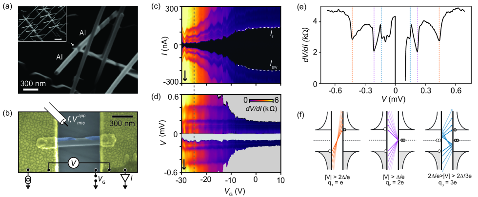
Figure 1c shows the differential resistance, , as a function of current through the device, , and back-gate voltage . A zero resistance supercurrent is observed for low . The current was swept from positive to negative (arrow) and the switching(re-trapping) current where the device transitions to(from) a resistive state from(to) the superconducting state is indicated. The differences in and are commonly observed in nanowire JJs3 and ascribed to a consequence of Joule heating in the dissipative regime and/or underdamped dynamics of the JJ43, 44. Both and decrease upon lowering as expected from a JJ with constant and an -type semiconductor which depletes with lowering . Here is the critical current and is the normal-state device resistance. The aperiodic oscillations in appearing in addition to the overall gate-dependence is attributed to universal conductance fluctuations in 3. At the normal state resistance is and , relatively close to the theoretical value , as previously reported for similar hybrids36. The measured excess current (Supporting Fig. S1) corresponds to a junction transmission of 45.
For above/below the zero-resistance region in Fig. 1c, exhibits a rich structure which follows the trend of and . To gain insight into the origin of these features, Fig. 1d shows the same data as a function of the measured voltage . Upon sweeping down from zero, the voltage remains until it abruptly switches at to a finite value. Therefore no data is obtained with below this value, and this region is greyed-out in Fig. 1d. Conversely, gradually decreases to zero around when sweeping down from positive values due to the underdamped junction dynamics,43, 44 enabling data extraction down to for . As expected for MAR, the structure in Fig. 1d appears at fixed voltages despite the variation in conductance with . Figure 1e shows a line trace of vs. for fixed . The three most pronounced dips are highlighted by dashed lines and follow (orange), (purple), and (blue) with consistent with prior results from 15 nm thick Al 46, 42, 36. This series is expected for MAR and the relevant processes transfer charges of and and are illustrated in Fig. 1f, where the slopes of the arrows represent voltage biases. Direct quasi particle tunneling occurs for . In the general case of , the order process involves Andreev reflections, a charge transfer of , and is allowed for . Suppression of processes occur for due to the low probability of Andreev reflection above the gap47. Overall, the dc transport characteristics in Fig. 1 are comparable to previous NW-based JJs3, 25, 48, 26.
We now consider the features arising from irradiating the device with microwaves. Figure 2a shows vs. and the rms amplitude, , of microwave radiation, as applied to the antenna (Fig. 1b). The gate voltage was fixed at as in Fig. 1e – similar features were observed at other , see Supporting Section II – and was swept from negative to positive. A series of ‘V’-shaped patterns are observed, fanning out from . The structure emerging from – i.e., when the JJ carries a supercurrent – is due to Shapiro steps49, 1 caused by phase-locking between the microwave field and the superconducting phase difference across the JJ leading to at step-wise increase of in units of . In Supporting Fig. S3, we replot this regime as a function as is common for studies of Shapiro steps, showing the conventional Shapiro pattern3, 50, 48, 51. The measurements are well-described by the extended RCSJ model and will not be considered further here.
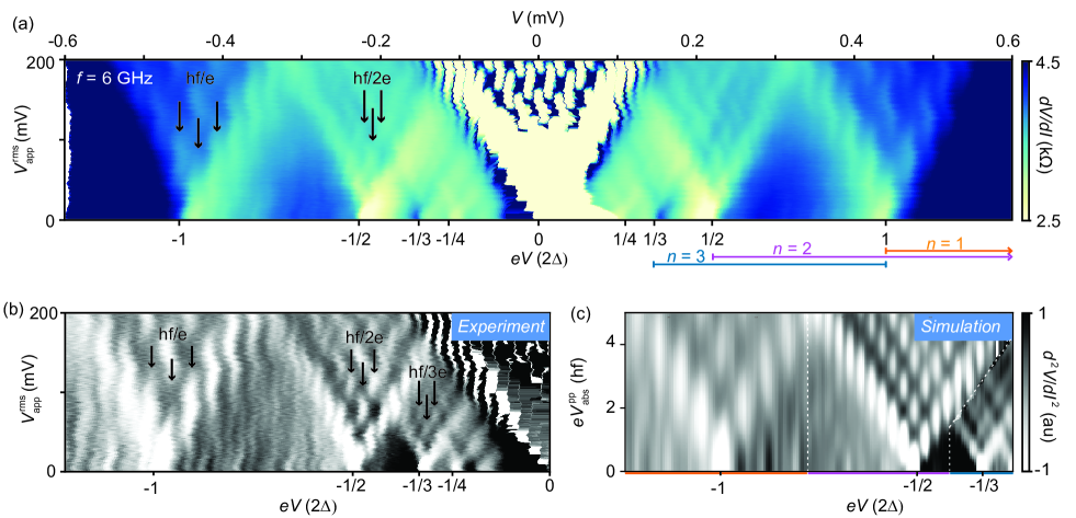
The remaining V-shaped structures in Fig. 2a, which evolve from the MAR features at finite , have a different origin and are the main focus of this work. Since the junction does not carry a supercurrent, phase locking and the resultant Shapiro steps do not occur. Instead, we attribute the structures to photon assisted tunneling. In general, for any two terminal device absorbing radiation at frequency , charges can absorb/emit photons and thereby gain energy and tunnel across the junction – here is the Planck constant and . Thus, at finite irradiation amplitude, the current at the dc voltage is related to the dc current in the absence of irradiation, , at . For smooth , this has no consequence, however, non-linearities in will repeat at finite radiation amplitude as sidebands with an intensity modulated by the radiation amplitude. In the simplest case where the radiation field on the sample is sinusoidal, , the current at finite radiation amplitude is given by the Tien-Gordon equation 34:
| (1) |
where is the Bessel function. The amplitude of each sideband oscillates with increasing according to (Supporting Fig. S4). This explains the overall shape of the structures in Fig. 2a which evolve from the non-linearities at associated with MAR. The highly asymmetric MAR features in Fig. 1e makes the inflection points of – i.e. peaks in – well suited for identifying the onset of MAR as shown in Fig. 2b. The modulation period of the features associated with the order MARs can be clearly resolved and as highlighted by the black arrows, the modulation period is not the same for each ‘V’-fan but rather decreases with decreasing bias. This is inconsistent with the conventional Tien-Gordon model described above which predicts the same characteristic pattern evolving from all non-linearities in . Instead, as discussed in the introduction, the pattern in Fig. 2a,b follows the work of Refs 32, 33 suggesting that Eq. 1 describes the microwave response for higher-order tunnel processes if the electron charge, , is replaced by the total transferred charge : Refs 32, 33 experimentally confirmed this for quasiparticle () and incoherent Cooper pair tunneling at zero bias (). For our case, the order MAR transfers electrons (Fig. 1f), and the corresponding modulation period should be . For this amounts to , , and for , respectively, in good agreement with the measured splittings ,, and from Fig. 2a,b (see below). Using this assumption we show in Fig. 2c the result of a simulation of taking the curve in absence of radiation as input and evolving according to Eq. 1 under the simplifying assumption that the order MAR dominate in the region around as shown by the dashed lines Fig. 2c (see Supporting Section IV for details). Comparing to Fig. 2b, the simulation accurately captures the main features of the measurement.
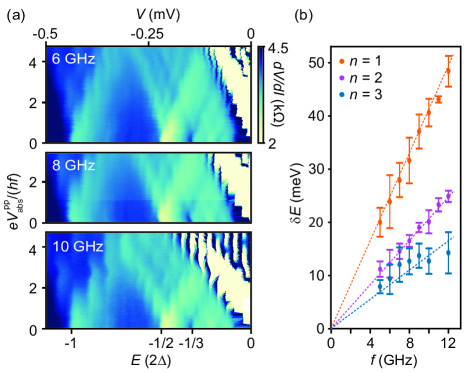
To further quantify the splitting, the measurements of Fig. 2a were repeated for different frequencies GHz. Three representative examples are shown in Fig. 3a for GHz. The coupling between the antenna and device depends strongly and non-monotonically on , and therefore the amplitude of absorbed radiation, in Fig. 3a was for visualization purposes normalized to the first zero of which occurs at (see Supporting information for non-normalized data at all eight frequencies). Figure 3b shows the average of the sideband spacing , as a function of (data points) and the theoretical relationship (dashed lines) for and 3 (blue, orange and green). The average was obtained across all the measured within each order, and the error bars represent the standard deviation. The good agreement between theory and experiment quantitatively confirms that the order MAR process involves the transmission of electrons across the junction.
In conclusion, we have studied the finite-bias sub-gap structure in epitaxial InAsSb/Al JJs under microwave radiation. We showed that the microwave response provides a sensitive probe of the transmitted charge up to order – i.e. a MAR process including two Andreev reflections. The modulation period was found to decrease with increasing MAR order, and the dependence of the sideband spacings on the radiation amplitude agrees quantitatively with the expectation that each order transmits electrons across the junction. A simulation based on a modified version of the Tien-Gordon equation was found to accurately reproduce the measurements. We expect the effect to be observable in non-epitaxially matched hybrids, albeit likely with less sharp features than observed here,42 and possibly modified weight of the MAR due to changes in the interface transmission.16 We believe that the results will be valuable tool for understanding the low-energy sub-gap spectrum in hybrid nanoscale devices. This becomes increasingly relevant with the rapid developments in the quality of hybrid quantum materials, device fabrication and filtering and measurement techniques, which allows for increasing coherence lengths and increased spectral resolution and thus even higher order MAR at progressively lower energies. Finally, the identification of sub-gap states is a crucial task for the powerful technique of spatially resolved superconducting scanning tunneling microscopy.
Acknowledgement This research was supported by the Danish National Research Foundation, Microsoft Quantum Materials Lab, and by research grants from Villum Fonden (00013157), The Danish Council for Independent Research (7014-00132), and European Research Council (866158).
Competing interests
The authors declare no competing interests.
Supporting Information
The supporting information contains additional data relating to the excess current, Shapiro steps, PAT of MAR at a different gate voltage, the underlying measurements for Fig. 3, as well as extra information regarding the simulation in Fig. 2c. This material is available free of charge via the internet at http://pubs.acs.org.
References
- Josephson 1962 Josephson, B. Possible new effects in superconductive tunnelling. Phys. Lett. 1962, 1, 251–253
- Kjaergaard et al. 2020 Kjaergaard, M.; Schwartz, M. E.; Braumüller, J.; Krantz, P.; Wang, J. I.-J.; Gustavsson, S.; Oliver, W. D. Superconducting Qubits: Current State of Play. Annu. Rev. Condens. Matter Phys. 2020, 11, 369–395
- Doh et al. 2005 Doh, Y.; van Dam, J.; Roest, A.; Bakkers, E.; Kouwenhoven, L.; De Franceschi, S. Tunable supercurrent through semiconductor nanowires. Science 2005, 309, 272–275
- Larsen et al. 2015 Larsen, T. W.; Petersson, K. D.; Kuemmeth, F.; Jespersen, T. S.; Krogstrup, P.; Nygård, J.; Marcus, C. M. Semiconductor-Nanowire-Based Superconducting Qubit. Phys. Rev. Lett. 2015, 115, 127001
- Hays et al. 2018 Hays, M.; de Lange, G.; Serniak, K.; van Woerkom, D. J.; Bouman, D.; Krogstrup, P.; Nygård, J.; Geresdi, A.; Devoret, M. H. Direct Microwave Measurement of Andreev-Bound-State Dynamics in a Semiconductor-Nanowire Josephson Junction. Phys. Rev. Lett. 2018, 121, 047001
- Oreg et al. 2010 Oreg, Y.; Refael, G.; von Oppen, F. Helical Liquids and Majorana Bound States in Quantum Wires. Phys. Rev. Lett. 2010, 105, 177002
- Lutchyn et al. 2010 Lutchyn, R. M.; Sau, J. D.; Das Sarma, S. Majorana Fermions and a Topological Phase Transition in Semiconductor-Superconductor Heterostructures. Phys. Rev. Lett. 2010, 105, 077001
- Giaever 1960 Giaever, I. Energy Gap in Superconductors Measured by Electron Tunneling. Phys. Rev. Lett. 1960, 5, 147–148
- Deacon et al. 2010 Deacon, R. S.; Tanaka, Y.; Oiwa, A.; Sakano, R.; Yoshida, K.; Shibata, K.; Hirakawa, K.; Tarucha, S. Tunneling Spectroscopy of Andreev Energy Levels in a Quantum Dot Coupled to a Superconductor. Phys. Rev. Lett. 2010, 104, 076805
- Pillet et al. 2010 Pillet, J.-D.; Quay, C. H. L.; Morfin, P.; Bena, C.; Yeyati, A. L.; Joyez, P. Andreev Bound States in Supercurrent-Carrying Carbon Nanotubes Revealed. Nature Phys 2010, 6, 965–969
- Chauvin et al. 2006 Chauvin, M.; vom Stein, P.; Pothier, H.; Joyez, P.; Huber, M. E.; Esteve, D.; Urbina, C. Superconducting Atomic Contacts under Microwave Irradiation. Phys. Rev. Lett. 2006, 97, 067006
- Heedt et al. 2021 Heedt, S. et al. Shadow-Wall Lithography of Ballistic Superconductor–Semiconductor Quantum Devices. Nat. Commun. 2021, 12, 4914
- Octavio et al. 1983 Octavio, M.; Tinkham, M.; Blonder, G.; Klapwijk, T. Subharmonic energy-gap structure in superconducting constrictions. Phys. Rev. B 1983, 27, 6739–6746
- Blonder et al. 1982 Blonder, G.; Tinkham, M.; Klapwijk, T. Transition from metallic to tunneling regimes in superconducting micro-constrictions - excess current, charge imbalance, and super-current conversion. Phys. Rev. B 1982, 25, 4515–4532
- Bratus et al. 1995 Bratus, E.; Shumeiko, V.; Wendin, G. Theory of subharmonic gap structure in superconducting mesoscopic tunnel contacts. Phys. Rev. Lett. 1995, 74, 2110–2113
- Averin and Bardas 1995 Averin, D.; Bardas, A. ac Josephson Effect in a Single Quantum Channel. Phys. Rev. Lett. 1995, 75, 1831–1834
- Kjaergaard et al. 2017 Kjaergaard, M.; Suominen, H. J.; Nowak, M. P.; Akhmerov, A. R.; Shabani, J.; Palmstrøm, C. J.; Nichele, F.; Marcus, C. M. Transparent Semiconductor-Superconductor Interface and Induced Gap in an Epitaxial Heterostructure Josephson Junction. Phys. Rev. Applied 2017, 7, 034029
- Scheer et al. 1998 Scheer, E.; Agrait, N.; Cuevas, J.; Yeyati, A.; Ludoph, B.; Martin-Rodero, A.; Bollinger, G.; van Ruitenbeek, J.; Urbina, C. The signature of chemical valence in the electrical conduction through a single-atom contact. Nature 1998, 394, 154–157
- Goffman et al. 2017 Goffman, M. F.; Urbina, C.; Pothier, H.; Nygård, J.; Marcus, C. M.; Krogstrup, P. Conduction Channels of an InAs-Al Nanowire Josephson Weak Link. New J. Phys. 2017, 19, 092002
- Buitelaar et al. 2003 Buitelaar, M.; Belzig, W.; Nussbaumer, T.; Babic, B.; Bruder, C.; Schönenberger, C. Multiple Andreev reflections in a carbon nanotube quantum dot. Phys. Rev. Lett. 2003, 91, 057005
- Eichler et al. 2007 Eichler, A.; Weiss, M.; Oberholzer, S.; Schönenberger, C.; Levy Yeyati, A.; Cuevas, J. C.; Martin-Rodero, A. Even-odd effect in Andreev transport through a carbon nanotube quantum dot. Phys. Rev. Lett. 2007, 99, 126602
- Sand-Jespersen et al. 2007 Sand-Jespersen, T.; Paaske, J.; Andersen, B. M.; Grove-Rasmussen, K.; Jorgensen, H. I.; Aagesen, M.; Sorensen, C. B.; Lindelof, P. E.; Flensberg, K.; Nygård, J. Kondo-enhanced Andreev tunneling in InAs nanowire quantum dots. Phys. Rev. Lett. 2007, 99, 126603
- Dolcini and Dell’Anna 2008 Dolcini, F.; Dell’Anna, L. Multiple Andreev Reflections in a Quantum Dot Coupled to Superconducting Leads: Effect of Spin-Orbit Coupling. Phys. Rev. B 2008, 78, 024518
- Hajer et al. 2019 Hajer, J.; Kessel, M.; Brüne, C.; Stehno, M. P.; Buhmann, H.; Molenkamp, L. W. Proximity-Induced Superconductivity in CdTe–HgTe Core–Shell Nanowires. Nano Lett. 2019, 19, 4078–4082
- Abay et al. 2014 Abay, S.; Persson, D.; Nilsson, H.; Wu, F.; Xu, H. Q.; Fogelström, M.; Shumeiko, V.; Delsing, P. Charge transport in InAs nanowire Josephson junctions. Phys. Rev. B 2014, 89, 214508
- Xiang et al. 2006 Xiang, J.; Vidan, A.; Tinkham, M.; Westervelt, R. M.; Lieber, C. M. Ge/Si nanowire mesoscopic Josephson junctions. Nat. Nanotechnol. 2006, 1, 208–213
- Peters et al. 2020 Peters, O.; Bogdanoff, N.; Acero González, S.; Melischek, L.; Simon, J. R.; Reecht, G.; Winkelmann, C. B.; von Oppen, F.; Franke, K. J. Resonant Andreev Reflections Probed by Photon-Assisted Tunnelling at the Atomic Scale. Nat. Phys. 2020, 16, 1222–1226
- Cuevas et al. 1999 Cuevas, J.; Martin-Rodero, A.; Yeyati, A. Shot noise and coherent multiple charge transfer in superconducting quantum point contacts. Phys. Rev. Lett. 1999, 82, 4086–4089
- Cron et al. 2001 Cron, R.; Goffman, M.; Esteve, D.; Urbina, C. Multiple-charge-quanta shot noise in superconducting atomic contacts. Phys. Rev. Lett. 2001, 86, 4104–4107
- Kozhevnikov et al. 2000 Kozhevnikov, A.; Schoelkopf, R.; Prober, D. Observation of photon-assisted noise in a diffusive normal metal-superconductor junction. Phys. Rev. Lett. 2000, 84, 3398–3401
- Ronen et al. 2016 Ronen, Y.; Cohen, Y.; Kang, J.-H.; Haim, A.; Rieder, M.-T.; Heiblum, M.; Mahalu, D.; Shtrikman, H. Charge of a quasiparticle in a superconductor. P. Natl. Acad. Sci. 2016, 113, 1743–1748
- Kot et al. 2020 Kot, P.; Drost, R.; Uhl, M.; Ankerhold, J.; Cuevas, J. C.; Ast, C. R. Microwave-Assisted Tunneling and Interference Effects in Superconducting Junctions under Fast Driving Signals. Phys. Rev. B 2020, 101, 134507
- Roychowdhury et al. 2015 Roychowdhury, A.; Dreyer, M.; Anderson, J. R.; Lobb, C. J.; Wellstood, F. C. Microwave Photon-Assisted Incoherent Cooper-Pair Tunneling in a Josephson STM. Phys. Rev. Applied 2015, 4, 034011
- Tien and Gordon 1963 Tien, P.; Gordon, J. Multiphoton process observed in interaction of microwave fields with tunneling between superconductor films. Phys. Rev. 1963, 129, 647
- Platero and Aguado 2004 Platero, G.; Aguado, R. Photon-assisted transport in semiconductor nanostructures. Phys. Rep. 2004, 395, 1–157
- Khan et al. 2020 Khan, S. A. et al. Highly Transparent Gatable Superconducting Shadow Junctions. ACS Nano 2020, 14, 14605–14615
- 37 Carrad, D. J.; Bjergfelt, M.; Kanne, T.; Aagesen, M.; Krizek, F.; Fiordaliso, E. M.; Johnson, E.; Nygård, J.; Jespersen, T. S. Shadow Epitaxy for In Situ Growth of Generic Semiconductor/Superconductor Hybrids. Adv. Mater. 32, 1908411
- Gazibegovic et al. 2017 Gazibegovic, S. et al. Epitaxy of advanced nanowire quantum devices. Nature 2017, 548, 434
- Krizek et al. 2017 Krizek, F.; Kanne, T.; Razmadze, D.; Johnson, E.; Nygård, J.; Marcus, C. M.; Krogstrup, P. Growth of InAs Wurtzite Nanocrosses from Hexagonal and Cubic Basis. Nano Lett. 2017, 17, 6090–6096
- Krogstrup et al. 2015 Krogstrup, P.; Ziino, N. L. B.; Chang, W.; Albrecht, S. M.; Madsen, M. H.; Johnson, E.; Nygård, J.; Marcus, C. M.; Jespersen, T. S. Epitaxy of semiconductor-superconductor nanowires. Nat. Mater. 2015, 14, 400–406
- Sestoft et al. 2018 Sestoft, J. E.; Kanne, T.; Gejl, A. N.; von Soosten, M.; Yodh, J. S.; Sherman, D.; Tarasinski, B.; Wimmer, M.; Johnson, E.; Deng, M.; Nygård, J.; Jespersen, T. S.; Marcus, C. M.; Krogstrup, P. Engineering Hybrid Epitaxial InAsSb/Al Nanowires for Stronger Topological Protection. Phys. Rev. Materials 2018, 2, 044202
- Chang et al. 2015 Chang, W.; Albrecht, S. M.; Jespersen, T. S.; Kuemmeth, F.; Krogstrup, P.; Nygård, J.; Marcus, C. M. Hard gap in epitaxial semiconductor–superconductor nanowires. Nat. Nanotechnol. 2015, 10, 232–236
- McCumber 1968 McCumber, D. E. Effect of ac Impedance on dc Voltage‐Current Characteristics of Superconductor Weak‐Link Junctions. Journal of Applied Physics 1968, 39, 3113–3118
- Tinkham et al. 2003 Tinkham, M.; Free, J. U.; Lau, C. N.; Markovic, N. Hysteretic I-V curves of superconducting nanowires. Phys. Rev. B 2003, 68, 134515
- Flensberg et al. 1988 Flensberg, K.; Hansen, J. B.; Octavio, M. Subharmonic energy-gap structure in superconducting weak links. Phys. Rev. B 1988, 38, 8707–8711
- Deng et al. 2016 Deng, M. T.; Vaitiekėnas, S.; Hansen, E. B.; Danon, J.; Leijnse, M.; Flensberg, K.; Nygård, J.; Krogstrup, P.; Marcus, C. M. Majorana bound state in a coupled quantum-dot hybrid-nanowire system. Science 2016, 354, 1557–1562
- Klapwijk et al. 1982 Klapwijk, T.; Blonder, G.; Tinkham, M. Explanation of subharmonic energy gap structure in superconducting contacts. Physica B+C 1982, 109-110, 1657–1664, 16th International Conference on Low Temperature Physics, Part 3
- Ridderbos et al. 2019 Ridderbos, J.; Brauns, M.; Li, A.; Bakkers, E. P. A. M.; Brinkman, A.; van der Wiel, W. G.; Zwanenburg, F. A. Multiple Andreev reflections and Shapiro steps in a Ge-Si nanowire Josephson junction. Phys. Rev. Materials 2019, 3, 084803
- Shapiro 1963 Shapiro, S. Josephson Currents in Superconducting Tunneling: The Effect of Microwaves and Other Observations. Phys. Rev. Lett. 1963, 11, 80–82
- Larson et al. 2020 Larson, T. F. Q.; Zhao, L.; Arnault, E. G.; Wei, M.-T.; Seredinski, A.; Li, H.; Watanabe, K.; Taniguchi, T.; Amet, F.; Finkelstein, G. Zero Crossing Steps and Anomalous Shapiro Maps in Graphene Josephson Junctions. Nano Letters 2020, 20, 6998–7003
- Perla et al. 2021 Perla, P.; Fonseka, H. A.; Zellekens, P.; Deacon, R.; Han, Y.; Kölzer, J.; Mörstedt, T.; Bennemann, B.; Espiari, A.; Ishibashi, K.; Grützmacher, D.; Sanchez, A. M.; Lepsa, M. I.; Schäpers, T. Fully in Situ Nb/InAs-nanowire Josephson Junctions by Selective-Area Growth and Shadow Evaporation. Nanoscale Adv. 2021, 3, 1413–1421