Mg2Si is the new black: introducing a black silicide with 95% average absorption at 200-1800 nm wavelengths
Abstract
Textured silicon surface structures, in particular black silicon (b-Si), open up possibilities for Si-based solar cells and photodetectors to be extremely thin and highly sensitive owing to perfect light-trapping and anti-reflection properties. However, near-infrared (NIR) performance of bare b-Si is limited by Si band gap of 1.12 eV or 1100 nm. This work reports a simple method to increase NIR absorption of b-Si by silicidation with magnesium. Obtained Mg2Si/b-Si heterostructure has a complex geometry where b-Si nanocones are covered by Mg2Si shells and crowned with flake-like Mg2Si hexagons. Mg2Si formation atop b-Si resulted in 5-fold lower reflectivity and optical absorption to be no lower than 88% over 200-1800 nm spectral range. More importantly, Mg2Si/b-Si heterostructure is more adjusted to match AM-1.5 solar spectrum with theoretically higher photogenerated current density. The maximal advantage is demonstrated in the NIR region compared to bare b-Si in full accordance with one‘s expectations about NIR sensitive narrow band gap (0.75 eV) semiconductor with high absorption coefficient, which is Mg2Si. Results of optical simulation confirmed the superiority of Mg2Si/b-Si NIR performance. Therefore, this new wide-band optical absorber called black silicide proved rather competitive alongside state-of-the-art approaches to extend b-Si spectral blackness.
I Introduction
Rigid semiconducting properties of the monocrystalline silicon (c-Si) place its single-junction solar cell (SC) efficiency to 29.4% Veith-Wolf et al. (2018) in accordance with Schockley-Queisser limitShockley and Queisser (1961). Interdigitated back contact approach set a practical milestone of 26.7% in 2017Yoshikawa et al. (2017). Recently, bifacial Si SC pushed it to approximately 29% closing the gap between theory and experimentUrl . Simultaneously, a gradual thinning of Si wafers for reduction of the panel cost takes place. This search for a thinner light absorbing layer is additionally motivated by the much wider flexible SC applicability Hashemi et al. (2020); Um et al. (2021); Zhao et al. (2021). Therefore, modern Si SC industry has been narrowed down to the motto “thinner & cheaper“ resulted in 10-fold decrease in thickness (20 m) Massiot et al. (2020) representing ultrathin SC niche and extremely thin (3 m) freestanding SC beating 12% efficiency Xue et al. (2020). However, the thinner an absorbing layer, the lower short-circuit current density is generated, while generally decrease in Si wafer thickness results in its open-circuit voltage increase. A compromised thickness of 75 m is believed to deliver a maximum photoelectric conversion efficiency of the Si SCChime et al. (2022). In addition, absorbing performance can be enhanced by light-trapping effect allowing to maintain thin and ultrathin designs providing higher photogenerated current density in comparison with the flat absorbersSaive (2021).
Black silicon (b-Si) is a material of choice for the both thickness reduction below 100 m toward flexible SC and light absorbing enhancement due to excellent trapping and antireflection propertiesOtto et al. (2015). On the other hand, b-Si photovoltaic performance below Si band gap (1.12 eV or 1100 nm) leaves a room for the further improvements. The lower an incident photon energy, the lower optical losses and associated absorbance despite of multiple reflections in black structures. Thus, it is expected that near-infrared (NIR) absorbing layer deposited above b-Si surface would result in extension of its spectral blackness . So far, b-Si structures have been modified thin film or nanoparticles deposition, formation of the hierarchical carbon-based nanostructures atop or pulsed laser postprocessing Lu et al. (2021); Isakov et al. (2018); Song et al. (2020); Wang et al. (2021); Sarkar et al. (2019); Shah et al. (2016); Phan and Yu (2020); Sánchez et al. (2021); Paulus et al. (2021). To date, practical use of the outlined approaches is limited by the low cost-efficiency factor resulted from the expensive deposition methods applied (atomic-layer deposition, molecular-beam epitaxy, ) and rare or high melting materials and compounds used (PtS2, NbN, Au, TiN and MoS2).
In this work, we propose a simple way to drastically increase b-Si NIR performance within thin coating of semiconducting (band gap 0.75 eV Mahan et al. (1996)) magnesium silicide (Mg2Si) by vacuum evaporation technique. Mg2Si is a Si-compatible optical material with superior absorbance from the ultraviolet (UV) to NIR regions compared to bare Si Kato et al. (2011). It has already demonstrated photovoltaic perspectives as homo-/heterojunction photodetectors and SC El-Amir et al. (2019a); Udono et al. (2015); El-Amir et al. (2019b); Zhu et al. (2021); Yu et al. (2021); Shevlyagin et al. (2020). Moreover, higher absorption coefficient exceeding 105 cm-1 above 1.5 eV Kato et al. (2011) is favorable for Si wafer thinning confirmed by recent Mg2Si/Si SC modeling Deng et al. (2017). In addition, proposed route to cover b-Si with NIR absorbing material is simple, low temperature, scalable and fast method resulted from the benefits of vacuum evaporation.
We show that vacuum evaporation results in b-Si geometry preservation and Mg2Si flakes-like epitaxial growth atop b-Si nanocones, higher NIR performance is a result of both hierarchical Mg2Si/b-Si structure and Mg2Si intrinsic absorption, Mg2Si coating resulted in only slight increase in UV-VIS reflection, while pronounced antireflection extends deeply below Si band gap down to that of Mg2Si, and (iv) overall optical performance can be maximized through appropriate silicidation conditions. Optical modeling of the Mg2Si/b-Si structure confirmed better localization of the NIR photons in comparison with uncovered b-Si. Finally, a survey on recent progress in b-Si modification in terms on NIR performance enhancement highlights new competitive black material with averaged over 200-1800 nm absorbance and reflectivity of 96% and 3.7%, respectively, called as black silicide.
II Experimental details.
Black Si samples used as initial substrates for silicidation were produced reactive-ion beam etching (RIE) as described elsewhereIvanova et al. (2013). RIE with SF6 and O2 mixture was performed to produce the nanocones with average height and period of 200 and 100 nm, respectively, on Si(001) wafer.
Next, b-Si samples were cleaned by a standard wafer cleaning process with piranha solution for 10 minutes prior to vacuum chamber loading. For the silicidation of the b-Si a high vacuum turbomolecular pumped evaporation chamber with the base pressure of 110-6 Torr was used. The chamber is equipped with K-cell for Mg evaporation (5N, Alfa Aesar, USA), quartz crystal microbalance (QCM) sensor and rotating sample s holder with resistive heater. QCM sensor was used for monitoring the deposition rate of Mg source. A calibration factor was obtained by comparing the thickness inferred from the QCM sensor with that of measured by atomic force microscopy on a specially step-shaped film deposited on bare Si(001) substrate. Before silicidation b-Si samples were degassed at 400oC for 20 minutes under the pressure no worse than 810-5 Torr. A two-step growth technique known as solid phase epitaxy (SPE) was applied for Mg2Si formation. First, 10-300 nm of Mg was deposited at room temperature with evaporation rate of 20 nm/min followed by sample annealing. The former resulted in metallic film formation on b-Si surface with pronounced light reflection contrasting to bare b-Si. It took about 5 minutes at 330-370 oC to obtain film color typical of Mg2Si. During the SPE, vacuum pressure was no worse than 310-6 Torr. After the sample unloading from the chamber, its morphology, crystal structure, chemical composition and optical properties were investigated.
The X-ray diffraction (XRD) studies were carried out in the 2/ mode and parallel beam optics geometry (RIGAKU SmartLab diffractometer, Japan). The XRD peaks were identified using the database ICDD PDF-2. Morphology of the Mg2Si/b-Si (black silicide) surface was characterized using scanning electron microscopy (SEM; Ultra 55+, Carl Zeiss, Germany). The crystal structure of prepared Mg2Si/b-Si structure were studied by means of high resolution transmission electron microscopy (HRTEM, TITAN 80-300, FEI Company, USA) operated at 300 kV voltage with point-to-point resolution of 0.165 nm. The energy-dispersive X-ray spectroscopy (EDS) analysis was carried out in the cross-sectional STEM mode, with the electron beam size of 1 nm. Raman scattering was pumped by a 473 nm CW laser using optical microscopy setup (NTEGRA Spectra II, NT-MDT, Russia) confocally aligned to a grating-type spectrometer with a thermo-electrically-cooled CCD-camera (i-Dus, Oxford Instruments, UK). The hemispheric total reflectance and transmittance for normal incidence in wavelength from 200 to 1800 nm were measured using a spectrophotometer with an integrating sphere (Cary 5000, Varian, USA). For comparison, reference spectra of bare b-Si were also obtained.
Finite-difference time-domain (FDTD) calculations have been carried out using commercial electromagnetic (EM) solver (Lumerical Solutions, Ansys Inc.). The morphology of the Mg2Si/b-Si heterostructure was reproduced from the corresponding cross-sectional STEM image. Local EM field distributions were calculated for the black silicide and pure b-Si structures pumped under normal incidence at 1300 nm wavelengths. Complex dielectric function of the Mg2Si was taken from Ref.Udono et al. (2015).
III Results and discussion.
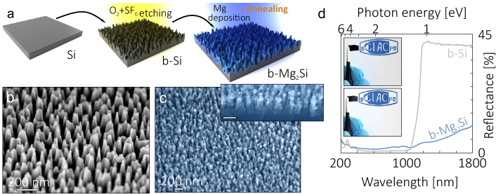
A template substrate for black magnesium silicide preparation was fabricated via reactive ion etching of monocrystalline Si wafer with (001) surface orientation. This procedure resulted in well-known b-Si structure composed of the randomly distributed Si nanocones. Next, vacuum evaporation to cover b-Si surface with Mg2Si layer was applied. Described protocol of the black silicide formation is illustrated in Fig.1a.
The as-loaded from vacuum chamber sample retains the typical nanocones structure of the bare b-Si shown in cross-sectional SEM images (Fig. 1b and c), whereas deposited Mg2Si layer of the optimal thickness (see discussions below) is presented as flake-like faceted hexagons crowning b-Si edges (inset of Fig. 1c). The reflectance spectrum of the Mg2Si covered b-Si nanocones array presented in Fig. 1d demonstrates strong NIR antireflection performance when compared to starting b-Si surface. These measurements confirm averaged reflection in the 200-1800 nm spectral range of 3.7% from black magnesium silicide surface, which is 5 times lower with respect to 17.6% of the bare b-Si. However, the former material clearly demonstrates slightly increased VIS reflection with specific silicide related spectral feature at 500 nm (2.5 eV) resulted from first direct interband optical transition in Mg2SiAu-Yang and Cohen (1969). This fact suggests that Mg2Si nanoflakes provide enough area for the surface reflection being the main reason behind slight deterioration of the VIS antireflection. Insets on Figure 1d demonstrate photographs of b-Si specimen after loading from vacuum evaporation chamber where silicidation took place. Grown Mg2Si/b-Si sample looks like uniform black surface to the naked eye. However, clear interface between bare (masked and uncovered with Mg2Si layer) b-Si area and Mg2Si film appears while sample tilting. Moreover, Mg2Si covering layer changes color from the black to deep blue intrinsic for silicide together with slightly higher VIS reflection further confirmed by optical measurements.
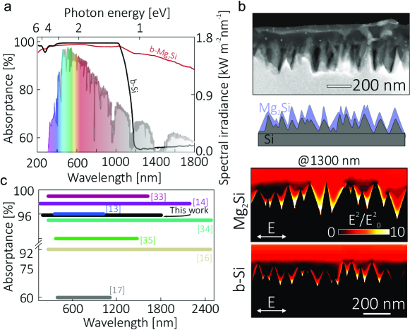
To illustrate the benefits of b-Si with Mg2Si layer in absorbing solar irradiance, optical transmittance (T) and reflectance (R) spectra were recorded from the ultraviolet (UV, 200 nm) to NIR (1800 nm) ranges (Figure 2a) and compared to state-of-the-art black surface structures Lu et al. (2021); Isakov et al. (2018); Wang et al. (2021); Sánchez et al. (2021); Pasanen et al. (2020); Zhong et al. (2016); Sheehy et al. (2007) (Figure 2c). Optical absorption spectra (A) calculated as 1-T-R demonstrate that optical properties of the b-Si changed drastically after Mg2Si deposition. In general, optical performance at ?1100 nm is significantly reduced in b-Si structures, while black silicide structure can effectively absorb NIR light resulted from the smaller Mg2Si band gap. Moreover, total reflection and absorption normalized to solar irradiance in accordance with expression:
| (1) |
where N() is solar flux under AM1.5G illumination, allowed us to conclude that black silicide structure under consideration is superior to bare b-Si in terms of NIR, overall and AM1.5G-normalized performance. Calculated values are summarized in Table 1.
|
|
|
|
|
|
|
|||||||||||||||
|---|---|---|---|---|---|---|---|---|---|---|---|---|---|---|---|---|---|---|---|---|---|
| b-Si | 17.56 | 38.56 | 29.8 | 81.1 | 58.3 | 92.1 | 50.9 | ||||||||||||||
| b-Mg2Si | 3.66 | 5.87 | 2.3 | 95.8 | 92.8 | 97.5 | 54 |
Let us pay attention only to the most impressive results obtained. For instance, black silicide structure demonstrates 6-fold decrease in NIR reflection being reduced from 38.5% down to 5.9% and 1.5 times higher NIR absorption. Moreover, Mg2Si/b-Si structure is better adjusted to match solar irradiance standard AM1.5G that reflected in 13-fold lower total reflection and higher averaged absorption of 97.5%. The latter allows to estimate the maximum achievable photo current density (MAPD) of the black silicide structure as:
| (2) |
where , , and are electron charge, Planck constant, velocity of light and photon wavelength, respectively. MAPD reaches 54 mA/cm2 under the assumption of recombination losses absent enhancing b-Si MAPD by 3 mA/cm2. This claims black silicide as solar energy material with enhanced performance beyond 1100 nm.
Next, FDTD calculations were performed to study the effect of b-Si covering with Mg2Si layer. Figure 2b represents geometry of the grown Mg2Si/b-Si heterostructure reconstructed from the HAADF SEM data. The cross-sectional EM field distributions (E2/E) near the surface of black silicide and bare b-Si under illumination are presented in the bottom panels of Figure 2b. The wavelength 1300 nm was chosen to illustrate NIR performance enhancement associated with NIR absorbing Mg2Si cover layer, while bare b-Si can demonstrate marked IR absorption only under heavily doping and/or laser postprocessing Paulus et al. (2021); Sheehy et al. (2007); Sher et al. (2014). Thus, performed optical modeling clearly answers the question concerning increased NIR absorption taking place in black silicide structure. Higher EM field localization and hot spots are observed in the case of Mg2Si/b-Si structure with maximum confinement occurred near the b-Si nanocones base and Mg2Si crowns. It can be tentatively concluded that complex hierarchical nanocones-nanoflake structure realized in black silicide resulted in the marked increase of the both NIR antireflection and absorption properties. NIR photons after being back-scattered within b-Si nanocones are effectively absorbed by Mg2Si possessing much higher intrinsic absorption coefficient over wide spectral range.
Significantly, the wide range optical absorption performance of the black silicide is compared with state-of-the-art approaches to enhance NIR efficiency of the b-Si as shown in Fig. 2c. One can see that black silicide delivers absorption of 96% over 200-1800 nm spectral range, while it does not require any expensive deposition methods and rare or high melting materials and compounds. For instance, PtS2 Lu et al. (2021) and NbN Isakov et al. (2018) decorated b-Si with superior absorption were produced under higher temperature budgets, while laser postprocessing of the b-Si often faces with Si amorphization Sánchez et al. (2021); Borodaenko et al. (2021), metastable phases formation and low minority carrier lifetime due to metal-like behavior after b-Si hyperdoppingSher et al. (2014); Winkler et al. (2011); Sickel et al. (2017).
The second part of our work gives some insights into relation between b-Mg2Si growth conditions and structural parameters as morphology, crystallinity and phase composition. On the other hand, these features strongly affect optical properties of the resulted nanostructures. Therefore, concerned markers were chosen to maximize wide-band antireflection and light absorbing performance of the black magnesium silicide.
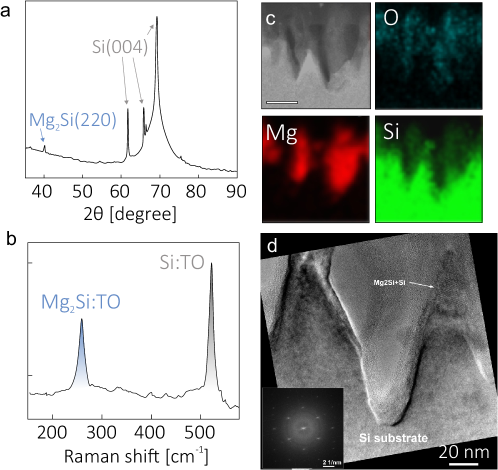
Structural and elemental analysis of the black silicide sample are summarized in Figure 3a-d. The XRD pattern and Raman spectra shown in Fig. 3a and b, respectively, suggest that b-Si sample cleaning and silicidation at moderate temperature of the solid state reaction (330oC) have no influence on b-Si intrinsic properties. XRD and Raman peak positions coincide well with bulk Si and no signs of amorphization are observed. It makes sense in terms of the well-known antireflection properties degradation of the RIE derived b-Si after thermal annealingCrouch et al. (2004). Neither metastable Mg-silicide phases, nor magnesium oxides, hydrates and silicates can be seen regardless low vacuum conditions. In addition, grown Mg2Si layer demonstrates good crystallinity resulting in only (220) diffraction peak appearance corresponded to Mg2Si with Fm3 crystal lattice and pronounced TO phonon mode observation with intensity comparable to that of Si, despite thin silicide film deposition. The former suggests that the grown Mg2Si shells have preferential orientation on the b-Si nanocones. Mg2Si crystallites mean size and residual stress were calculated to be 28 nm and 0.2%, respectively in accordance with XRD data. Thus, Mg2Si cover layer does not disgrace the best ultrahigh vacuum grown Mg2Si films in terms of crystallinity, whereas much lower vacuum and substrate surface treatment requirements were used Mahan et al. (1996); Shevlyagin et al. (2020); Vantomme et al. (1997); Gouralnik et al. (2018, 2021). These facts confirm high applicability and scalability degrees of the proposed new black material preparation. HAADF-STEM imaging and EDS elemental mapping (Fig. 3c) have been carried out to illustrate Mg2Si/b-Si morphology and chemical composition. These findings confirm that Mg2Si/b-Si sample is a stacked textured structure with Mg2Si layer repeating b-Si nanocones geometry to some extent. Elemental oxygen is related to atmosphere long-term exposure. A closer look at the individual b-Si nanocones covered with Mg2Si is shown in the HRTEM image (Figure 3d). Magnesium silicide is presented with few-nm thick crystalline shell surrounding b-Si nanocones with well-defined reflexes on FFT inset. Thus, Mg2Si/b-Si material is a hierarchically organized nanostructure where b-Si nanocones are covered with thin Mg2Si shells and crowned by Mg2Si nanoflakes.
To find the optimal conditions for Mg2Si growth atop b-Si, Mg2Si/b-Si samples s crystallinity, morphology, phase composition and optical properties were investigated depending on deposited Mg film thickness and substrate temperature upon solid phase epitaxy. The former varied from 10 to 300 nm and the latter did in 250-450oC temperature range.
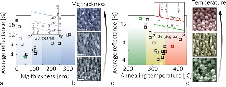
When fixing SPE temperature slightly above 300 oC, which is favorable for magnetron sputtering and thermal evaporation of Mg2Si films on Si substrates El-Amir et al. (2019b); Yu et al. (2013); Katagiri et al. (2018); Zhang et al. (2017), resulting coated b-Si nanostructures demonstrate non monotonic antireflection behavior (defined as averaged on 200-1800 nm optical reflectance) with increase in Mg layer thickness (see Fig. 4a, main frame). First, one can see an abrupt decrease in reflection as Mg thickness approaches 50 nm being a global minimum with the best antireflection performance. Representative morphology evolution of the Mg2Si/b-Si heterostructures is shown in series of the cross-sectional SEM images in Fig. 4b. Passing global minimum of the Mg2Si/b-Si reflectance, the thicker deposited Mg film, the lower antireflection is demonstrated. This tendency resulted from Mg2Si nanoflakes enlargement and increase in surface reflection from it. At higher thickness almost continuous Mg2Si film is observed. In addition, Mg2Si nanoflakes enlargement resulted in higher intensity of the main Mg2Si (220) and other (200), (111) and (311) diffraction peaks appearance suggested polycrystalline Mg2Si growth atop b-Si nanocones (inset of Fig. 4a). As a result, thin Mg films of about 50 nm in thickness are of interest in terms of the best antireflection properties. It corresponds to formation of a complex Mg2Si/b-Si nanostructures upon SPE annealing, which preserves b-Si light-trapping geometry extending its spectral blackness .
At the second stage, effect of the SPE temperature on the average reflectivity of the Mg2Si/b-Si was examined for the fixed 50-nm thick Mg film thickness determined previously as optimal. The data are summarized in Fig. 4c showing that minimal reflectance is achieved at 330 oC. Interestingly, temperature below 270 oC is not enough for complete silicidation of the b-Si nanocones. XRD data (inset of Fig. 4c) clearly demonstrate contribution from metallic hexagonal Mg with (0002) and (10) reflexes. In contrast, when annealing temperature exceeds 370 oC, low vacuum condition used resulted in Mg oxidation rather than silicide formation. It reflects in diffraction from (200) crystal plane of the cubic MgO plane and absence of any Mg2Si related phonon modes in Raman measurements. In addition, in both cases the surface morphology changed to popcorn like structure (Figure 4d) resulting in increase of the total reflectance. Therefore, low temperature (330 oC) solid phase epitaxy of the thin (50 nm) Mg film atop b-Si structure are both required to modify its optical properties toward NIR blackness .
IV Conclusion
In summary, a simple and low-cost method for boosting NIR absorption performance of black silicon by integrating with magnesium silicide is demonstrated. Resulting Mg2Si/b-Si heterostructure preserves antireflection and light-trapping properties of the b-Si associated with nanocones-like geometry and expands its spectral blackness from 1100 nm to at least 1800 nm owning to NIR sensitive narrow-band-gap Mg2Si cover layer. Explored and verified by modeling optical properties of this new wide-band black material called black silicide suggest some possible applications ranging from NIR optical absorbers, high-sensitive NIR devices and solar cells. Results obtained propose material scientists, especially dealing with Si-silicide tandem solar cells engineering, a simple technology to enhance photoelectric conversion efficiency using a b-Si as a platform for silicidation with other environment-friendly and Si-compatible silicides, for example BaSi2 or -FeSi2.
V Declaration of Competing Interest
The authors declare that they have no known competing financial interests or personal relationships that could have appeared to influence the work reported in this paper.
VI Acknowledgements
This research was supported by the Russian Science Foundation under Grant No. 20-72-00006. Authors are thankful to Prof. Saulius Juodkazis from Optical Sciences Centre and ARC Training Centre in Surface Engineering for Advanced Materials, School of Science, Swinburne University of Technology for providing bare black Si samples.
VII References
References
- Veith-Wolf et al. (2018) B. A. Veith-Wolf, S. Schäfer, R. Brendel, and J. Schmidt, Solar Energy Materials and Solar Cells 186, 194 (2018).
- Shockley and Queisser (1961) W. Shockley and H. J. Queisser, Journal of applied physics 32, 510 (1961).
- Yoshikawa et al. (2017) K. Yoshikawa, H. Kawasaki, W. Yoshida, T. Irie, K. Konishi, K. Nakano, T. Uto, D. Adachi, M. Kanematsu, H. Uzu, et al., Nature energy 2, 1 (2017).
- (4) “https://www.anu.edu.au/news/all-news/anu-scientists-set-new-record-with-bifacial-solar-cells, accessed: May, 2022,” .
- Hashemi et al. (2020) S. A. Hashemi, S. Ramakrishna, and A. G. Aberle, Energy & Environmental Science 13, 685 (2020).
- Um et al. (2021) H.-D. Um, I. Hwang, D. Choi, and K. Seo, Accounts of Materials Research 2, 701 (2021).
- Zhao et al. (2021) J. Zhao, J. Zha, Z. Zeng, and C. Tan, Journal of Materials Chemistry A (2021).
- Massiot et al. (2020) I. Massiot, A. Cattoni, and S. Collin, Nature Energy 5, 959 (2020).
- Xue et al. (2020) M. Xue, K. N. Nazif, Z. Lyu, J. Jiang, C.-Y. Lu, N. Lee, K. Zang, Y. Chen, T. Zheng, T. I. Kamins, et al., Nano Energy 70, 104466 (2020).
- Chime et al. (2022) U. Chime, L. Wolf, V. Buga, D. Weigand, A. Gad, J. Köhler, A. Lambertz, W. Duan, K. Ding, T. Merdzhanova, et al., Solar RRL 6, 2100594 (2022).
- Saive (2021) R. Saive, Progress in Photovoltaics: Research and Applications 29, 1125 (2021).
- Otto et al. (2015) M. Otto, M. Algasinger, H. Branz, B. Gesemann, T. Gimpel, K. Füchsel, T. Käsebier, S. Kontermann, S. Koynov, X. Li, et al., Advanced optical materials 3, 147 (2015).
- Lu et al. (2021) J. Lu, W. Zhuang, W. Yang, X. Zhang, G. Su, X. Gong, J. Yuan, J. Sui, Y. Zhou, G. Zhang, et al., The Journal of Physical Chemistry C 125, 27335 (2021).
- Isakov et al. (2018) K. Isakov, A. P. Perros, A. Shah, and H. Lipsanen, Nanotechnology 29, 335303 (2018).
- Song et al. (2020) Y. Song, T. Liu, S. Liu, J. Huang, J. Li, C. Tian, T. Yu, Y. He, Y. Liu, and Z. Zhong, Journal of Materials Science: Materials in Electronics 31, 4696 (2020).
- Wang et al. (2021) K. Wang, S. Liu, J. Li, S. Wu, J. Xia, J. Chen, C. Tian, Y. Liu, and Z. Zhong, Journal of Materials Science: Materials in Electronics 32, 11503 (2021).
- Sarkar et al. (2019) A. Sarkar, S. Mukherjee, A. K. Das, and S. K. Ray, Nanotechnology 30, 485202 (2019).
- Shah et al. (2016) A. Shah, P. Stenberg, L. Karvonen, R. Ali, S. Honkanen, H. Lipsanen, N. Peyghambarian, M. Kuittinen, Y. Svirko, and T. Kaplas, Scientific reports 6, 1 (2016).
- Phan and Yu (2020) T. L. Phan and W. J. Yu, Scientific reports 10, 1 (2020).
- Sánchez et al. (2021) M. I. Sánchez, P. Delaporte, Y. Spiegel, B. Franta, E. Mazur, and T. Sarnet, physica status solidi (a) 218, 2000550 (2021).
- Paulus et al. (2021) S. Paulus, P. Mc Kearney, F. Völklein, and S. Kontermann, AIP Advances 11, 075014 (2021).
- Mahan et al. (1996) J. E. Mahan, A. Vantomme, G. Langouche, and J. P. Becker, Physical Review B 54, 16965 (1996).
- Kato et al. (2011) T. Kato, Y. Sago, and H. Fujiwara, Journal of Applied Physics 110, 063723 (2011).
- El-Amir et al. (2019a) A. A. El-Amir, T. Ohsawa, T. Nabatame, A. Ohi, Y. Wada, M. Nakamura, X. Fu, K. Shimamura, and N. Ohashi, Materials Science in Semiconductor Processing 91, 222 (2019a).
- Udono et al. (2015) H. Udono, H. Tajima, M. Uchikoshi, and M. Itakura, Japanese Journal of Applied Physics 54, 07JB06 (2015).
- El-Amir et al. (2019b) A. A. El-Amir, T. Ohsawa, S. Ishii, M. Imura, M. Liao, X. Fu, H. Segawa, I. Sakaguchi, T. Nagao, K. Shimamura, et al., Materials Science in Semiconductor Processing 102, 104577 (2019b).
- Zhu et al. (2021) Q. Zhu, P. Ye, Y. Tang, X. Zhu, Z. Cheng, J. Xu, and M. Xu, Nanotechnology 33, 115202 (2021).
- Yu et al. (2021) H. Yu, L. Sun, S. Ji, R. Deng, Z. Mo, and Q. Xie, IEEE Photonics Journal 14, 1 (2021).
- Shevlyagin et al. (2020) A. Shevlyagin, I. Chernev, N. Galkin, A. Gerasimenko, A. Gutakovskii, H. Hoshida, Y. Terai, N. Nishikawa, and K. Ohdaira, Solar Energy 211, 383 (2020).
- Deng et al. (2017) Q. Deng, Z. Wang, S. Wang, and G. Shao, Solar Energy 158, 654 (2017).
- Ivanova et al. (2013) E. P. Ivanova, J. Hasan, H. K. Webb, G. Gervinskas, S. Juodkazis, V. K. Truong, A. H. Wu, R. N. Lamb, V. A. Baulin, G. S. Watson, et al., Nature communications 4, 1 (2013).
- Au-Yang and Cohen (1969) M. Au-Yang and M. L. Cohen, Physical Review 178, 1358 (1969).
- Pasanen et al. (2020) T. P. Pasanen, J. Isometsä, M. Garin, K. Chen, V. Vähänissi, and H. Savin, Advanced Optical Materials 8, 2000047 (2020).
- Zhong et al. (2016) H. Zhong, A. Guo, G. Guo, W. Li, and Y. Jiang, Nanoscale research letters 11, 1 (2016).
- Sheehy et al. (2007) M. A. Sheehy, B. R. Tull, C. M. Friend, and E. Mazur, Materials Science and Engineering: B 137, 289 (2007).
- Sher et al. (2014) M.-J. Sher, C. B. Simmons, J. J. Krich, A. J. Akey, M. T. Winkler, D. Recht, T. Buonassisi, M. J. Aziz, and A. M. Lindenberg, Applied Physics Letters 105, 053905 (2014).
- Borodaenko et al. (2021) Y. Borodaenko, S. Syubaev, S. Gurbatov, A. Zhizhchenko, A. Porfirev, S. Khonina, E. Mitsai, A. V. Gerasimenko, A. Shevlyagin, E. Modin, et al., ACS Applied Materials & Interfaces 13, 54551 (2021).
- Winkler et al. (2011) M. T. Winkler, D. Recht, M.-J. Sher, A. J. Said, E. Mazur, and M. J. Aziz, Physical Review Letters 106, 178701 (2011).
- Sickel et al. (2017) J. Sickel, A. Ahrens, A. Baumann, W. Schade, S. Kontermann, and M. Seibt, physica status solidi (a) 214, 1700264 (2017).
- Crouch et al. (2004) C. H. Crouch, J. Carey, M. Shen, E. Mazur, and F. Genin, Applied Physics A 79, 1635 (2004).
- Vantomme et al. (1997) A. Vantomme, J. E. Mahan, G. Langouche, J. P. Becker, M. Van Bael, K. Temst, and C. Van Haesendonck, Applied physics letters 70, 1086 (1997).
- Gouralnik et al. (2018) A. Gouralnik, A. Maslov, A. Y. Ustinov, S. Dotsenko, A. Shevlyagin, I. Chernev, V. Il’yashenko, S. Kitan, E. Koblova, K. Galkin, et al., Applied Surface Science 439, 282 (2018).
- Gouralnik et al. (2021) A. S. Gouralnik, A. V. Shevlyagin, I. M. Chernev, A. Y. Ustinov, A. V. Gerasimenko, and A. K. Gutakovskii, Materials Chemistry and Physics 258, 123903 (2021).
- Yu et al. (2013) H. Yu, Q. Xie, and Q. Chen, Journal of Materials Science: Materials in Electronics 24, 3768 (2013).
- Katagiri et al. (2018) A. Katagiri, S. Ogawa, M. Uehara, P. Sankara Rama Krishnan, M. Kurokawa, M. Matsushima, T. Shimizu, K. Akiyama, and H. Funakubo, Journal of materials science 53, 5151 (2018).
- Zhang et al. (2017) B. Zhang, T. Zheng, Q. Wang, Y. Zhu, H. N. Alshareef, M. J. Kim, and B. E. Gnade, Journal of Alloys and Compounds 699, 1134 (2017).