Hole Mobility Calculation for Monolayer Molybdenum Tungsten Alloy Disulfide
Abstract
A simple band model using higher order non-parabolic effect was adopted for single layer molybdenum tungsten alloy disulfide (i.e., ). The first-principles method considering supercell was used to study band structure of single layer alloy and a simple band (i.e., effective mass approximation model, EMA) model with higher order non-parabolic effect was used to fit the first-principle band structures in order to calculate corresponding the hole mobility. In addition, we investigate the alloy scattering effect on the hole mobility of .
I Introduction
Among the typical transition-metal dichalcogenide (TMD) alloys, single layer molybdenum tungsten alloy disulfide has a characteristic atomically thin two-dimensional layered structure that contributes to its unique electronic properties, allowing its application in transistor device technology. As the band gap of TMD alloys can be altered, these alloys can be suitably applied in band-gap engineering for transistor devices. In order to develop novel -type field effect transistor (PFET), it is crucial to consider how the type of TMD alloy used affects its band structure and the corresponding hole mobility. Two types of TMD alloy single layers are discussed in our previous work. As an example of the first type, molybdenum tungsten alloy disulfide (Mo1-xWxS2), with its two-dimensional layered structure, has great potential application in future transistor technology. TMD alloys may have better intermiscibility, and the synthesis of TMD bulk alloys with multiple layers, such as Mo1-xWxS2 [1, 2], imparts good thermodynamic stability to the material. In a previous study [3], the analysis of single layer Mo1-xWxS2 by scanning transmission electron microscopy (TEM) revealed its homo-atomic and hetero-atomic coordinates. Moreover, the quantified degree of alloying of the transition metals such as W and Mo was successfully obtained and their alloying mechanism in the single layer was identified. In another recent study [4], the first family of atomic-single layer Mo1-xWxS2 was exfoliated and the x-dependent photoluminescence (PL) was observed from the single layer alloy Mo1-xWxS2. Further, the composition-dependent physical properties of single layer Mo1-xWxS2, including its band structure and effective mass, were determined by the first-principles calculation using a large supercell with an effective band structure (EBS) approximation model [5, 6].
It was found that as the W composition increases, the effective mass of the hole decreases; this is because of the similar contributions of MoS2 and WS2 to valence bands. Smaller effective mass is favorable for hole mobility. Thus, we aim to explore the hole mobility of the monolayer Mo1-xWxS2 for PFET application. A simple band model cannot effectively calculate the valence band structure of single layer alloy Mo1-xWxS2. Therefore, development of a compact valence band model for single layer alloy Mo1-xWxS2 considering the calculation of hole mobility is crucial. In this study, we propose a compact valence band structure and hole mobility calculation model for the Mo1-xWxS2 single layer. Section II presents the supercell first principle band structure of Mo1-xWxS2 single layer, a simple band model, and hole mobility calculation of single layer Mo1-xWxS2. Section III discusses the results of the experiments conducted in this study. Finally, Section IV presents the conclusions of this study.
II Computation Methods
II.1 First-Principles Method
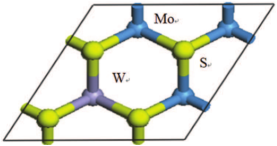
In this work, we used the Vienna Ab Initio Simulation Package (VASP) considering the projector augmentedwave (PAW) potentials to calculate the band structure of monolayer Mo1-xWxS2. Note that density functional theory (DFT) was used with local density approximation (LDA) exchange–correlation functional, and eV cutoff energy for plane-wave expansion. We also used k-grid mesh of the supercell, and set the electronic self-consistent cycles of energy convergence criterion to eV. The spin orbit coupling was not including in our work because prediction with the inclusion of spin orbit coupling provided smaller band gap of WS2 than that of MoS2. To model single layer Mo1-xWxS2, a supercell (including atoms) was set up for three W mole fraction values of , with , , and . Our choice of the supercell is reasonable as the same trend is attained as obtained by the supercell mentioned in a previous work [6]. Figure 1 shows a supercell of monolayer Mo0.75W0.25S2 in the plane adopted in this work.
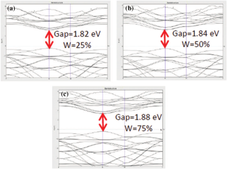
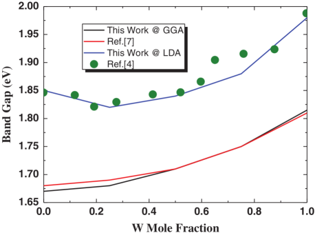
In Figure 2, there are three first principle band structures of single layer alloy Mo1-xWxS2 with three W values of 25, 50, and 75%. The band gap of single layer MoS2 could be varied by alloying transition metal atoms. The Mo1-xWxS2 solutions remain as the direct bandgap semiconductors and the constituents of monolayer WS2 and monolayer MoS2. Band gap of single layer alloy Mo1-xWxS2 versus W composition is shown in Figure 3. Note that with increasing W mole fraction, initially, the band gap of single layer alloy Mo1-xWxS2 decreased gradually, and then from onward, a rapid increase was observed until the band gap reached that of the single layer WS2. These results are consistent with the band gaps experimentally measured in terms of PL [4]. Note that the generalized gradient approximation (GGA) considering the PBE function is typically adopted for the first-principles DFT calculation of the Mo1-xWxS2 band gaps and for the comparison of results. A comparison indicated that our results are consistent with those of Wei et al. [7]. We decided to use LDA to replace GGA in our work because LDA fitted experimental data better than did GGA.
II.2 Compact Valence Bond Model
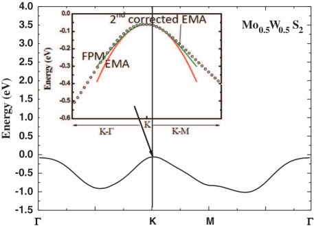
As described in the previous subsection, the first principle band structure of single layer alloy Mo1-xWxS2 was calculated considering the supercell in calculation [6]. Figure 4 indicates that within an extremely small energy region, the valence band structure is ideal parabolic-like in valley due to the isotropic and parabolic dispersion feature of the holes in the valance band. The hole mobility is determined by the valence band described by a simple band model such as an effective mass approximation (EMA) band model with different effective mass along and direction, as shown in Eq. (1).
| (1) |
where is the in-plane wave vector; and are, respectively, the effective masses in the top valence band including key -points such as , and .
However, the simple EMA model cannot accurately determine the band structure of single layer alloy Mo1-xWxS2 in the entire -region. Therefore, it is required that the hole mobility of single layer Mo1-xWxS2 be calculated using an improved compact valence band model. Hosseini et al. [8] used simple band model considering the first-order non-parabolic factor , as shown in Eq. (2):
| (2) |
In our study, we adopted a higher-order correction for the simple band model of the hole band of silicon, as described in Ref. [9]. Thus, we built a compact simple valence band model for single layer Mo1-xWxS2 alloys by considering high-order non-parabolic factors and ,as shown in Eq. (3):
| (3) |
and were obtained by fitting the first principle band structure for the top valence band.
II.3 Hole Mobility Calculation for Single Layer Alloy
Based on an established method of semiconductor materials carrier mobility calculation [10], we calculated the hole mobility of Mo1-xWxS2 alloy using the Kubo-Greenwood formula, given by Eqs. (4)-(6).
| (4) |
| (5) |
| (6) |
where denotes the density of states for single layer alloy Mo1-xWxS2, is the group velocity with energy dependence along the direction [11], means the Fermi–Dirac distribution, denotes carrier energy, and as shown in Eq. (4) means the total scattering time. Further, denotes dependent group velocity and means carrier transport direction. The different scattering rates from phonon and alloy effects are summed using Matthiessen’s rule in order to determine the total scattering rate and the impact of various scattering mechanisms including phonon and alloy scattering:
| (7) |
Here, is owing to alloy scattering, whereas the remaining two terms are related to phonon scattering. Moreover, the scattering rates owing to optical and acoustic phonon scattering, namely and , respectively, for single layer Mo1-xWxS2 alloys were adopted from the previous study [12]. We followed the alloy scattering formula proposed by Ref. [13] to calculate alloy scattering rate, and scattering formula is given by Eq. (8).
| (8) |
where is the alloy scattering potential, which can be determined by the difference in the valence band offsets between monolayer MoS2 and WS2 or the metal work function difference between Mo and W. denotes the area of the unit cell and means alloy composition of W in single layer alloy Mo1-xWxS2.
III Results and Discussion
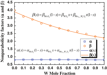
The top valence band of single layer alloy Mo0.5W0.5S2 calculated using the supercell first-principle method is shown in Figure 4. Further, we compare the results of the conventional simple band model and the proposed improved model with the high-order non-parabolic effect. There is no major difference in the velocity square and density of states calculations between the two methods, thus indicating that the proposed compact band model with the high-order non-parabolic effect provides effective and better mobility calculation without comprising accuracy. Figure 5 shows the plot of the non-parabolic factors and calculated by Eq. (3) with respect to the mole fraction of W in single layer Mo1-xWxS2. As you can see that is dependent on alloy composition of W and is nearly independent of W. The inset of Figure 5 shows the data fitted using a high-order polynomial. Note that no severe bowing effect is observed, especially for the non-parabolic factor .
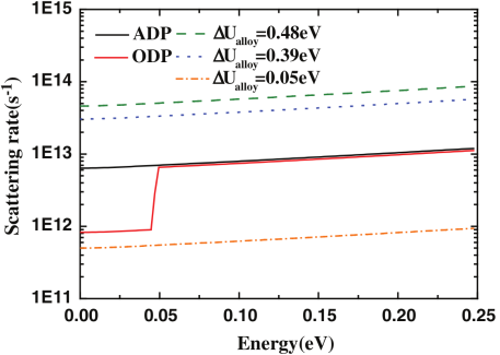
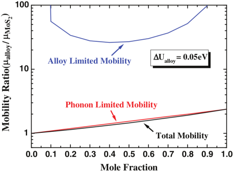
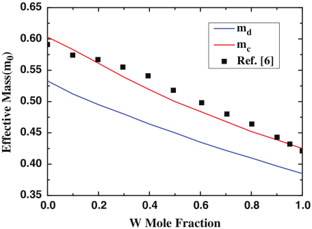
Figure 6 shows the variation of the hole effective mass, namely conductivity effective mass (denoted as ; Eq. (3), where is )and density of states effective mass (denoted as ; Eq. (3), ), versus W mole fraction. The figure indicates that both effective mass values decrease almost linearly with increasing alloy composition of W owing to higher effective mass of single layer MoS2 as compare to that of single layer WS2. In addition, is higher than possibly because of the trigonal warping effect of the valence band.
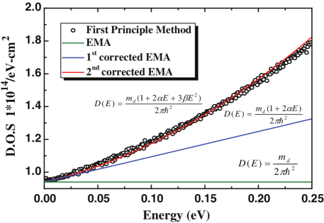
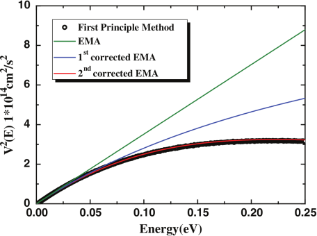
Figures 7 and 8 present velocity square and density of states values versus energy for monolayer alloy Mo0.5W0.5S2, respectively. The figures indicate that velocity square and density of states calculations using the simple band model with the high-order non-parabolic effect agree well with the results from the first-principles method. Therefore, the simple EMA band model with higher order non-parabolic effect is the optimal option to calculate hole mobility.
Futher, Figure 9 shows the comparison of two hole scattering rates such as optical and acoustic phonon scattering and alloy scattering with three different alloy potentials.
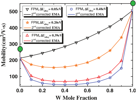
Figure 10 shows alloy limited mobility, phonon limited mobility and total mobility ratios of the single layer alloy Mo1-xWxS2 with eV. We found that phonon limited mobility ratio increases up to when W mole function is 100%, while it was less than the alloy limited mobility ratio for the entire range of W mole fractions. Thus, the effect of alloy scattering is not prominent owing to phonon scattering is higher than alloy scattering. The hole mobility versus alloy composition of W considering different values of alloy scattering potential is shown in Figure 11. As you can see in Figure 11, alloy scattering potential values of and eV were adopted from the valence band offsets between MoS2 and WS2 [15, 16]. We also compare our results with the theoretical results of Ref. [14]. Further, our results agree with those of Ref. [14]. From Figure 11, we observe that the hole mobility for the single layer Mo1-xWxS2 with eV is the best because of the negligible alloy-limited scattering. A higher value of eV results in mobility less than 1 (with respect to MoS2), mainly because of the severe alloy scattering and lower hole mobility than in case of pure single layer MoS2.
IV Conclusions
We investigated the alloy effect on the hole mobility of single layer alloy Mo1-xWxS2. We determined the band gap of single layer alloy Mo1-xWxS2 from supercell first-principle calculation; further, we used a simple band model as well as a hole mobility calculation for single layer alloy Mo1-xWxS2. The simple valence band model can be applied to the TCAD design study of next generation electron devices that use monolayer molybdenum tungsten alloy disulfide as the channel material.
Acknowledgements.
Authors all appreciate supporting of the Ministry of Science and Technology, Taiwan, R.O.C., under contract numbers MOST 108-2622-8-002-016, 106-2221-E-005-096-MY3, and 106-2221-E-005-097-MY3 and also thank to Uni-edit (www.uni-edit.net) for English proofreading and editing this manuscript.References
- Dumcenco et al. [2010] D. O. Dumcenco, K.-Y. Chen, Y.-P. Wang, Y.-S. Huang, and K.-K. Tiong, Raman study of 2H-Mo1-xWxS2 layered mixed crystals, Journal of Alloys and Compounds 506, 940 (2010).
- Komsa and Krasheninnikov [2012] H.-P. Komsa and A. V. Krasheninnikov, Two-dimensional transition metal dichalcogenide alloys: Stability and electronic properties, J. Phys. Chem. Lett. 3, 3652 (2012).
- Dumcenco et al. [2013] D. O. Dumcenco, H. Kobayashi, Z. Liu, Y.-S. Huang, and K. Suenaga, Visualization and quantification of transition metal atomic mixing in Mo1-xWxS2 single layers, Nature Communications 4, 1 (2013).
- Chen et al. [2013] Y. Chen, J. Xi, D. O. Dumcenco, Z. Liu, K. Suenaga, D. Wang, Z. Shuai, Y.-S. Huang, and L. Xie, Tunable band gap photoluminescence from atomically thin transition-metal dichalcogenide alloys, ACS Nano 7, 4610 (2013).
- Popescu and Zunger [2012] V. Popescu and A. Zunger, Extracting versus effective band structure from supercell calculations on alloys and impurities, Phys. Rev. B 85, 085201 (2012).
- Xi et al. [2014] J. Xi, T. Zhao, D. Wang, and Z. Shuai, Tunable electronic properties of two-dimensional transition metal dichalcogenide alloys: A first-principles prediction, J. Phys. Chem. Lett. 5, 285 (2014).
- Wei et al. [2014] X.-L. Wei, H. Zhang, G.-C. Guo, X.-B. Li, W.-M. Lau, and L.-M. Liu, Modulating the atomic and electronic structures through alloying and heterostructure of single-layer MoS2, J. Mater. Chem. A 2, 2101 (2014).
- Hosseini et al. [2015] M. Hosseini, M. Elahi, M. Pourfath, and D. Esseni, Strain-induced modulation of electron mobility in single-layer transition metal dichalcogenides MX2 (M=Mo,W;X=S,Se), IEEE Transactions on Electron Devices 62, 3192 (2015).
- Ridley [2013] B. K. Ridley, Quantum Processes in Semiconductors (Oxford University Press, 2013).
- Chang [2006] S.-T. Chang, Electron and hole mobilities in orthorhombically strained silicon, Japanese Journal of Applied Physics 45, 3070 (2006).
- Fu et al. [1994] Y. Fu, K. Grahn, and M. Willander, Valence band structure of GexSi1-x for hole transport calculation, IEEE Transactions on Electron Devices 41, 26 (1994).
- Chen et al. [2018] K.-T. Chen, R.-Y. He, C.-F. Lee, M.-T. Wu, and S.-T. Chang, Compact conduction band model for transition-metal dichalcogenide alloys, Microelectronics Reliability 83, 223 (2018).
- Harrison and Hauser [1976] J. W. Harrison and J. R. Hauser, Alloy scattering in ternary III-V compounds, Phys. Rev. B 13, 5347 (1976).
- Jin et al. [2014] Z. Jin, X. Li, J. T. Mullen, and K. W. Kim, Intrinsic transport properties of electrons and holes in monolayer transition-metal dichalcogenides, Phys. Rev. B 90, 045422 (2014).
- Özçelik et al. [2016] V. O. Özçelik, J. G. Azadani, C. Yang, S. J. Koester, and T. Low, Band alignment of two-dimensional semiconductors for designing heterostructures with momentum space matching, Phys. Rev. B 94, 035125 (2016).
- Kang et al. [2013] J. Kang, S. Tongay, J. Zhou, J. Li, and J. Wu, Band offsets and heterostructures of two-dimensional semiconductors, Applied Physics Letters 102, 012111 (2013).