First Principle Study for Optical Properties of TMDC/Graphene Heterostructures
Abstract
The transition-metal dichalcogenide (TMDC) in the family of (; ) and the graphene () monolayer are an atomically thin semiconductor and a semimetal, respectively. The monolayer has been discovered as a new class of semiconductors for electronics and optoelectronics applications. Because of the hexagonal lattice structure of both materials, and are often combined with each other to generate van der Waals heterostructures. Here, the heterostructures are investigated theoretically based on density functional theory (DFT). The electronic structure and the optical properties of four different heterostructures are computed. We systematically compare these heterostructures for their complex permittivity, absorption coefficient, reflectivity and refractive index.
I Introduction
Materials in confined geometries are hosts to novel phenomena. For example, in one dimension (1D), the fractional charge excitation or the soliton is found in the electronic properties of the organic polyacetylene [1], and the Haldane conjecture [2], which corresponds to the symmetry-protected topological phase, is experimentally found in the spin-1 magnetic chain, e.g., CsNiCl3, [Ni(HF2)(3-Clpyradine)4]BF4, Ni(C2H8N2)2NO2(ClO4) and Y2BaNiO5 [3, 4, 5, 6, 7, 8]. Quantum states conversion through entanglement manipulations [9] as well as new types of quantum phase transitions with a negative central charge [10] are among the recently investigated 1D systems.
Examples of novel physical phenomena in two dimension (2D) include quantum Hall systems in semiconductors [11], the supersolid phase of atomic systems in the optical lattice [12, 13] and Dirac electrons in graphene [14]. Graphene (Gr) is one of the most widely investigated 2D materials; it possesses a high mobility [15, 16, 17, 18, 19] and is driven by Dirac cone dispersions near the Fermi level at the K-point and the K’-point in the hexagonal Brillouin zone[20]. However, the gapless nature of Gr limits its applications in the semiconductor industry. Therefore, finding new 2D materials with a large band gap is an interesting topic. Note that a new allotropy of carbon, the 2D biphenylene monolayer, was discovered very recently [21, 22, 23, 24].
In addition to the carbon, a number of 2D materials with an energy band gap have been synthesized, including the quantum spin Hall insulator HgTe [25, 26], free-standing silicene [27] and the transition-metal dichalcogenide (TMDC) family. Monolayer TMDCs [28, 29, 30, 31, 32, 33, 34, 35, 36, 37, 38, 39], such as molybdenum disulfide (MoS2) [40, 41], molybdenum diselenide (MoSe2) [42], tungsten disulfide (WS2) [43] and tungsten diselenide (WSe2) [44, 45], have been found to be direct gap semiconductors [46] and have emerged as new optically active materials for novel device applications. The TMDCs in the family of MX2, where and , have a rather large energy band gap compared to HgTe and silicene; thus, these materials are more versatile as candidates for thin, flexible device applications and useful for a variety of applications including transistors [47], lubrication [48], lithium-ion batteries [49] and thermoelectric devices [50]. Other TMDCs, e.g., PbTaSe2, MoxW1-xTe2 and NiTe2, can exhibit more unusual physical properties such as topological superconductivity and Dirac and Weyl semimetal physics [51, 52, 53, 54, 55, 56]. Two-dimensional hydrogenated NiTe2, PdS2, PdSe2, and PtSe2 monolayers also exhibit a quantum anomalous Hall effect [57].
One of the approaches used to broaden the application of 2D materials is to form a heterostructure in which similar lattice structures for different monolayers are usually required, e.g., the hexagonal lattices of TMDC, Gr, boron nitride [58], and boron phosphide (BP) [59]. It has been suggested that MX2/BP heterostructures have a good ability for optical absorption [59]. On the other hand, the MX2/Gr of the type-I van der Waals heterostructures have attracted much attention for their electronic properties. Research on MoS2/Gr [60, 61, 62], MoSe2/Gr [63, 64, 65], WS2/Gr [66] and WSe2/Gr [67, 68] has revealed that MX2/Gr is favorable for electronics applications and field-effect transistors. However, there are relatively few studies on its optical properties [69, 70, 71]; therefore, comprehensive research on the optical properties of MX2/Gr is desired.
In this communication, we theoretically investigate the optical properties of MX2/Gr heterostructures. By means of a density functional theory simulation, we systematically compare the energy band structures, the density of states, complex permittivity, absorption coefficients, reflectivity, and refraction indexes.
II Materials and Methods
| /Gr | /Gr | /Gr | /Gr | /Gr |
|---|---|---|---|---|
| mismatch ratio | 1.83% | 0.10% | 2.04% | 0.01% |
| meV | meV | meV | meV |
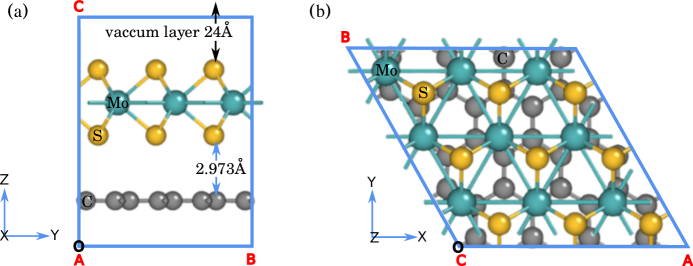
The first-principles calculations are based on the local-density approximation (LDA) proposed by Kohn and Sham [72], which approximates the total energy of the multielectron system. The simulations were implemented using the software package Nanodcal and its accompanying software packages DeviceStudio and OpticCal [73, 74]. A plane wave basis was set with a cutoff energy of Hartree and a -centered -points grid. The atomic structures were relaxed until the force was smaller than eV/Å and the total energy convergence criterion was set as eV. In order to avoid interactions in the vertical direction between neighboring slabs, a vacuum layer of 24 Å was added between different slabs.
| /Gr | Mo-S | Mo-C | S-C | C-C | -Gr |
|---|---|---|---|---|---|
| 2.404Å | 4.826Å | 3.089Å | 1.600Å | 2.973Å | |
| /Gr | Mo-Se | Mo-C | Se-C | C-C | -Gr |
| 2.349Å | 4.920Å | 3.270Å | 1.626Å | 3.161Å | |
| /Gr | W-S | W-C | S-C | C-C | -Gr |
| 2.379Å | 4.774Å | 3.078Å | 1.596Å | 2.954Å | |
| /Gr | W-Se | W-C | Se-C | C-C | -Gr |
| 2.354Å | 4.940Å | 3.286Å | 1.625Å | 3.178Å |
The lattice constants of the MoS2, MoSe2, WS2, WSe2 and Gr monolayers were 3.166 Å, 3.288 Å, 3.153 Å, 3.282 Å and 2.47 Å, respectively[32, 63]. For all the MX2/Gr heterostructures, lattice mismatch ratios less than 5% were achieved by choosing a MX2 supercell and a Gr supercell, as shown in Figure 1. The details of the lattice mismatch ratios are listed in Table 1. After the structure optimization, the lattice contents were 9.668 Å, 9.854 Å, 9.648 Å and 9.845 Å for MoS2/Gr, MoSe2/Gr, WS2/Gr and WSe2/Gr, respectively. The details of the atom–atom distances as well as the layer–Gr layer distances are listed in Table 2. The total number of atoms in the simulations was 59 for MX2/Gr, 27 for the monolayer of MX2, and 32 for the monolayer of Gr.
The binding energies are calculated by the energy difference between the heterostructures and the monolayers:
| (1) |
where , and are the total energies of the heterostructures, isolated MX2 and Gr, respectively. It is interesting to compare other heterostructures, such as MX2/BP [59], as regards binding energies. The interface binding energies of the most stable configurations of MoS2/BP, MoSe2/BP, WS2/BP and WSe2/BP are meV, meV, meV and meV, respectively, [59]. As listed in Table 1, all the binding energies for the MX2/Gr heterostructures in this study are negative, and the values are close to MX2/BP, demonstrating that the structural stability of MX2/Gr is similar to that of MX2/BP.
III Results
III.1 Band structures
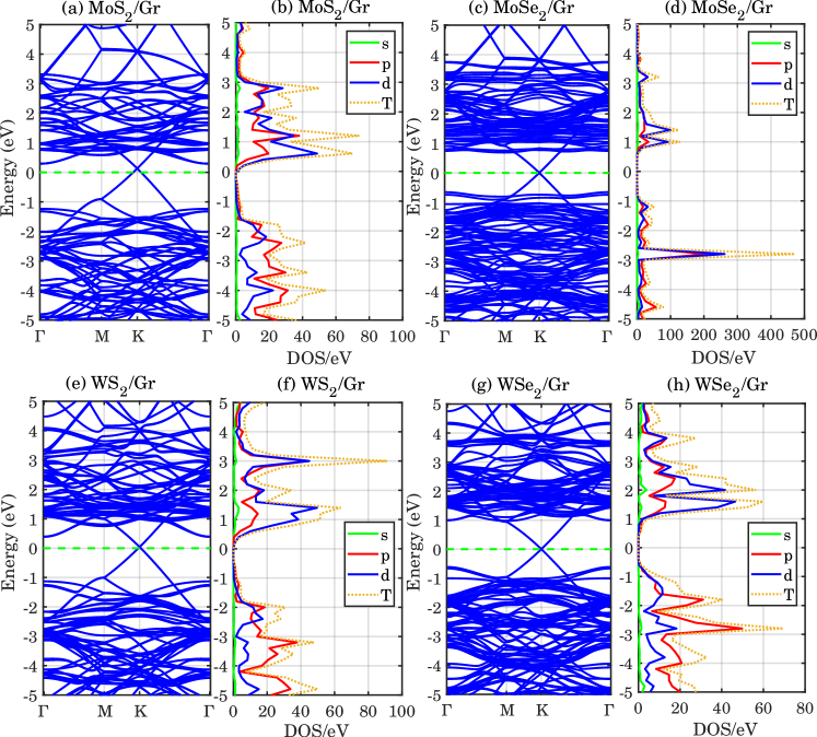
The direct band gaps of the MoS2, MoSe2, WS2 and WSe2 monolayers were eV, eV, eV and eV, respectively, [36], where both the conduction band minimum (CBM) and the valence band maximum (VBM) were at the K-point in the Brillouin zone. The Dirac point of the Gr was located at the K-point and pinned to the Fermi level. All the results of the energy band structures for the MX2 monolayers are consistent with the existing literature [35, 17]. Now we report the energy band structures and the electronic density of states (DOS) for the four MX2/Gr, as shown in Figure 2. We found that the band structure of MX2/Gr could basically be regarded as the overlap of the band structures of the MX2 and Gr monolayers. Due to van der Waals interactions, the Dirac point opens a small gap of meV, meV, meV and meV for MoS2/Gr, MoSe2/Gr, WS2/Gr and WSe2/Gr, respectively. The total and partial DOS values of MX2/Gr are also shown in Figure 2. The partial DOS is the relative contribution of a particular orbital to the total DOS. The d-orbital contributions mainly come from the W or Mo atoms, and the p-orbital contributions come from S or Se, and C atoms. Contributions from the s-orbital are minimal. These results reflect a fairly weak interfacial coupling at the interface between MX2 and Gr.
The Schottky contacts are formed between the semiconducting MX2 and the metallic Gr. The Schottky barrier is one of the most important characteristics of a semiconductor–metal junction and dominates the transport properties. Based on the Schottky–Mott model [75, 76, 77], at the interface of the metal and semiconductor, an n-type Schottky barrier height (SBH) is defined as the energy difference between the Fermi level and the conduction band minimum , i.e., . Similarly, the p-type SBH is defined as the energy difference between and the valence band maximum , i.e., . The n/p-type Schottky contacts are classified by the smaller SBH. The SBH are and for MoS2/Gr, and for MoSe2/Gr, and for WS2/Gr, and and for WSe2/Gr, respectively. Therefore, MoS2/Gr, MoSe2/Gr, WS2/Gr and WSe2/Gr are the n-type, p-type, n-type and p-type Schottky contacts, respectively[64, 66, 67].
III.2 Optical properties
In order to understand the optical properties, the complex permittivity or the so-called dielectric function was computed under the long-wave approximation, i.e., . The complex permittivity as a function of incident photon energy is [78]
| (2) |
where is the electron charge, is the vacuum permittivity, is the electron mass, is the direction of the vector potential, is the momentum operator, is the photon energy, and and are the Fermi–Dirac distribution functions. Since , i.e., , the refraction index and the extinction coefficient are obtained:
| (3) |
| (4) |
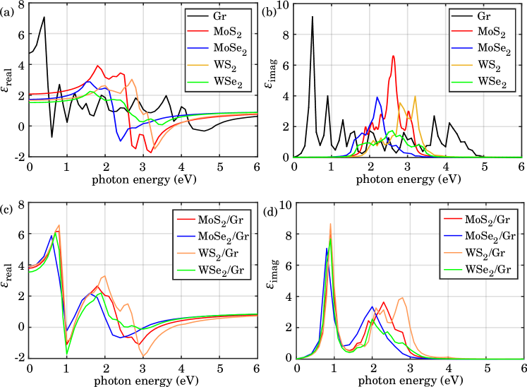
The real part is caused by various kinds of displacement polarization inside the material and represents the energy storage term of the material. The imaginary part is related to the absorption of the material, including gain and loss. Therefore, the permittivity must be real in the absence of the incident photon energy, i.e., . It is expected that the smaller the energy gap of a material, the larger its . On the other hand, since the DOS only appears in a finite range of energy in the numerical simulation, electron transitions by the absorption of photons do not occur if the photon energy is too large. Therefore, without photon absorption the computed is close to zero in the large limit of the incident photon energy, and the permittivity approaches a constant real value.
In Figure 3, we show the real part and the imaginary part of the complex permittivity for MX2/Gr heterostructures and MX2 and Gr monolayers. Since the energies corresponding to the peak positions of the DOS in the conduction and valence bands of the MX2/Gr were smaller than those of MX2, the peak positions of the real part of MX2/Gr in Fig. 3(c) had a red shift compared with the MX2 in Fig. 3(a). The highest peak corresponding energy of the imaginary part of the MX2/Gr in Fig. 3(d) was about 0.8 eV to 0.9 eV, which corresponds to the position where the real part decreases the fastest.
After obtaining the dielectric function, the absorption coefficient is computed by
| (5) |
and the reflectivity is
| (6) |
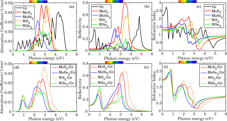
Figure 4 compares MX2/Gr, MX2 and Gr for their absorption coefficient , reflectivity and refractive index . Since MX2/Gr has a smaller optical band gap compared with the MX2 monolayer, MX2/Gr has a wider range of light absorption, from eV to eV. As shown in Fig. 4(b),(e), MX2/Gr had a higher reflectivity than MX2 in the infrared area (), and had a higher reflectivity than Gr in the visible light area. We compare the real part of the permittivity of monolayer MX2 in Fig. 3(a) with the refractive index of monolayer MX2 in Fig. 4(c), and compare the real part of the permittivity of the MX2/Gr heterostructure in Fig. 3(c) with that of MX2/Gr in Fig. 4(f). It was found that the changing trends from Fig. 3(a) to Fig. 4(c) are similar to those from Fig. 3(c) to Fig. 4(f). This means that the real part of the dielectric constant dominates the effect of the refractive index. The above simulation results suggest that MX2/Gr heterostructures are good candidate materials for optical applications.
IV Discussion
Two-dimensional heterostructures based on TMDCs exhibit the enhancement of electrical and optoelectrical properties, which are promising for next-generation optoelectronics devices. We systematically computed the complex permittivity , absorption coefficient , reflectivity and refractive index for MX2/Gr heterostructures, where M = Mo, W; and X = S, Se. Our results qualitatively agree with those from previous studies on MoS2/Gr [69] and WSe2/Gr [70], where red shifts in the , and were found compared with MoS2 and WSe2 monolayers. We extended the investigations to other MX2/Gr heterostructures, and found qualitatively similar behavior in their optical properties.
It is worth comparing our MX2/Gr results with the recent simulation results on the MX2/BP in terms of absorption abilities [59]. Although different types of van der Waals heterostructures were found in MX2/BP (type-I for MoS2/BP and WS2/BP; type-II for MoSe2/BP and WSe2/BP), all the materials of MX2/BP have excellent absorption abilities in the infrared and visible light range, i.e., to for the wavelength [59]. In our study, all the MX2/Gr were type-I heterostructures, and the values of the absorption coefficients were in the same range compared with MX2/BP in the infrared and visible light range. Therefore, MX2/Gr can be utilized as alternative materials for the applications of solar optoelectronics devices.
Acknowledgements.
CHY is grateful to Dr. Yu-Chin Tzeng for his invaluable discussions and helps.References
- Su et al. [1979] W. P. Su, J. R. Schrieffer, and A. J. Heeger, Phys. Rev. Lett. 42, 1698 (1979).
- Haldane [1983] F. D. M. Haldane, Phys. Rev. Lett. 50, 1153 (1983).
- Xu et al. [1996] G. Xu, J. F. DiTusa, T. Ito, K. Oka, H. Takagi, C. Broholm, and G. Aeppli, Phys. Rev. B 54, R6827 (1996).
- Buyers et al. [1986] W. J. L. Buyers, R. M. Morra, R. L. Armstrong, M. J. Hogan, P. Gerlach, and K. Hirakawa, Phys. Rev. Lett. 56, 371 (1986).
- Renard et al. [1987] J. P. Renard, M. Verdaguer, L. P. Regnault, W. A. C. Erkelens, J. Rossat-Mignod, and W. G. Stirling, Europhysics Letters 3, 945 (1987).
- Tzeng [2012] Y.-C. Tzeng, Phys. Rev. B 86, 024403 (2012).
- Tzeng et al. [2017] Y.-C. Tzeng, H. Onishi, T. Okubo, and Y.-J. Kao, Phys. Rev. B 96, 060404 (2017).
- Pajerowski et al. [2022] D. M. Pajerowski, A. P. Podlesnyak, J. Herbrych, and J. Manson, Phys. Rev. B 105, 134420 (2022).
- Tzeng et al. [2016] Y.-C. Tzeng, L. Dai, M. Chung, L. Amico, and L.-C. Kwek, Sci. Rep. 6, 26453 (2016).
- Tu et al. [2022] Y.-T. Tu, Y.-C. Tzeng, and P.-Y. Chang, SciPost Phys. 12, 194 (2022).
- Klitzing et al. [1980] K. v. Klitzing, G. Dorda, and M. Pepper, Phys. Rev. Lett. 45, 494 (1980).
- Ng et al. [2010] K.-K. Ng, Y.-C. Chen, and Y.-C. Tzeng, J. Phys.: Cond. Mat. 22, 185601 (2010).
- Chen and Yang [2017] Y.-C. Chen and M.-F. Yang, Journal of Physics Communications 1, 035009 (2017).
- Geim [2009] A. K. Geim, Science 324, 1530 (2009).
- Bolotin et al. [2008] K. I. Bolotin, K. J. Sikes, Z. Jiang, M. Klima, G. Fudenberg, J. Hone, P. Kim, and H. L. Stormer, Solid State Communications 146, 351 (2008).
- Chan et al. [2008] K. T. Chan, J. B. Neaton, and M. L. Cohen, Phys. Rev. B 77, 235430 (2008).
- Torbatian and Asgari [2018] Z. Torbatian and R. Asgari, Applied Sciences 8, 238 (2018).
- Koukaras et al. [2015] E. N. Koukaras, G. Kalosakas, C. Galiotis, and K. Papagelis, Sci. Rep. 5, 12923 (2015).
- Wendler et al. [2015] F. Wendler, A. Knorr, and E. Malic, Nanophotonics 4, 224 (2015).
- Castro Neto et al. [2009] A. H. Castro Neto, F. Guinea, N. M. R. Peres, K. S. Novoselov, and A. K. Geim, Rev. Mod. Phys. 81, 109 (2009).
- Fan et al. [2021] Q. Fan, L. Yan, M. W. Tripp, et al., Science 372, 852 (2021).
- Al-Jayyousi et al. [2022] H. K. Al-Jayyousi, M. Sajjad, K. Liao, and N. Singh, Sci. Rep. 12, 4653 (2022).
- Bafekry et al. [2021] A. Bafekry, M. Faraji, M. M. Fadlallah, H. R. Jappor, S. Karbasizadeh, M. Ghergherehchi, and D. Gogova, J. Phys.: Cond. Mat. 34, 015001 (2021).
- Ren et al. [2022] K. Ren, H. Shu, W. Huo, Z. Cui, and Y. Xu, Nanotechnology 33, 345701 (2022).
- Bernevig et al. [2006] B. A. Bernevig, T. L. Hughes, and S.-C. Zhang, Science 314, 1757 (2006).
- König et al. [2007] M. König, S. Wiedmann, C. Brüne, A. Roth, H. Buhmann, L. W. Molenkamp, X.-L. Qi, and S.-C. Zhang, Science 318, 766 (2007).
- Vogt et al. [2012] P. Vogt, P. De Padova, C. Quaresima, J. Avila, E. Frantzeskakis, M. C. Asensio, A. Resta, B. Ealet, and G. Le Lay, Phys. Rev. Lett. 108, 155501 (2012).
- Coleman et al. [2011] J. N. Coleman, M. Lotya, A. O’Neill, S. D. Bergin, P. J. King, U. Khan, K. Young, A. Gaucher, S. De, R. J. Smith, I. V. Shvets, S. K. Arora, G. Stanton, H.-Y. Kim, K. Lee, G. T. Kim, G. S. Duesberg, T. Hallam, J. J. Boland, J. J. Wang, J. F. Donegan, J. C. Grunlan, G. Moriarty, A. Shmeliov, R. J. Nicholls, J. M. Perkins, E. M. Grieveson, K. Theuwissen, D. W. McComb, P. D. Nellist, and V. Nicolosi, Science 331, 568 (2011).
- Latzke et al. [2015] D. W. Latzke, W. Zhang, A. Suslu, T.-R. Chang, H. Lin, H.-T. Jeng, S. Tongay, J. Wu, A. Bansil, and A. Lanzara, Phys. Rev. B 91, 235202 (2015).
- Hsu et al. [2017] W.-T. Hsu, L.-S. Lu, D. Wang, J.-K. Huang, M.-Y. Li, T.-R. Chang, Y.-C. Chou, Z.-Y. Juang, H.-T. Jeng, L.-J. Li, et al., Nature Communications 8, 1 (2017).
- Zhang et al. [2014] Y. Zhang, T.-R. Chang, B. Zhou, Y.-T. Cui, H. Yan, Z. Liu, F. Schmitt, J. Lee, R. Moore, Y. Chen, H. Lin, H.-T. Jeng, S.-K. Mo, Z. Hussain, A. Bansil, and Z.-X. Shen, Nature Nanotechnology 9, 111 (2014).
- Yang et al. [2022] C.-H. Yang, Y.-F. Chung, Y.-S. Su, K.-T. Chen, Y.-S. Huang, and S.-T. Chang, J. Comput. Electron. 21, 571 (2022).
- Kumar and Schwingenschlogl [2015] S. Kumar and U. Schwingenschlogl, Chemistry of Materials 27, 1278 (2015).
- Kormányos et al. [2015] A. Kormányos, G. Burkard, M. Gmitra, J. Fabian, V. Zólyomi, N. D. Drummond, and V. Fal’ko, 2D Materials 2, 022001 (2015).
- Cheiwchanchamnangij and Lambrecht [2012] T. Cheiwchanchamnangij and W. R. L. Lambrecht, Phys. Rev. B 85, 205302 (2012).
- Haldar et al. [2015] S. Haldar, H. Vovusha, M. K. Yadav, O. Eriksson, and B. Sanyal, Phys. Rev. B 92, 235408 (2015).
- Gusakova et al. [2017] J. Gusakova, X. Wang, L. L. Shiau, A. Krivosheeva, V. Shaposhnikov, V. Borisenko, V. Gusakov, and B. K. Tay, Physica Status Solidi A 214, 1700218 (2017).
- Molina-Sánchez and Wirtz [2011] A. Molina-Sánchez and L. Wirtz, Phys. Rev. B 84, 155413 (2011).
- Gu and Yang [2014] X. Gu and R. Yang, Applied Physics Letters 105, 131903 (2014).
- Chang et al. [2014] T.-R. Chang, H. Lin, H.-T. Jeng, and A. Bansil, Sci. Rep. 4, 6270 (2014).
- Splendiani et al. [2010] A. Splendiani, L. Sun, Y. Zhang, T. Li, J. Kim, C.-Y. Chim, G. Galli, and F. Wang, Nano letters 10, 1271 (2010).
- Helmrich et al. [2021] S. Helmrich, K. Sampson, D. Huang, M. Selig, K. Hao, K. Tran, A. Achstein, C. Young, A. Knorr, E. Malic, U. Woggon, N. Owschimikow, and X. Li, Phys. Rev. Lett. 127, 157403 (2021).
- Gutiérrez et al. [2013] H. R. Gutiérrez, N. Perea-López, A. L. Elías, A. Berkdemir, B. Wang, R. Lv, F. López-Urías, V. H. Crespi, H. Terrones, and M. Terrones, Nano Letters 13, 3447 (2013).
- Zhou et al. [2015] H. Zhou, C. Wang, J. C. Shaw, R. Cheng, Y. Chen, X. Huang, Y. Liu, N. O. Weiss, Z. Lin, Y. Huang, and X. Duan, Nano Letters 15, 709 (2015).
- Liu et al. [2019] R.-Y. Liu, M.-K. Lin, P. Chen, T. Suzuki, P. C. J. Clark, N. K. Lewis, C. Cacho, E. Springate, C.-S. Chang, K. Okazaki, W. Flavell, I. Matsuda, and T.-C. Chiang, Phys. Rev. B 100, 214309 (2019).
- Mak et al. [2010] K. F. Mak, C. Lee, J. Hone, J. Shan, and T. F. Heinz, Phys. Rev. Lett. 105, 136805 (2010).
- Yoon et al. [2011] Y. Yoon, K. Ganapathi, and S. Salahuddin, Nano Letters 11, 3768 (2011).
- Lee et al. [2010] C. Lee, Q. Li, W. Kalb, X.-Z. Liu, H. Berger, R. W. Carpick, and J. Hone, Science 328, 76 (2010).
- Chang and Chen [2011] K. Chang and W. Chen, Chem. Commun. 47, 4252 (2011).
- Jobayr and Salman [2021] M. R. Jobayr and E. M.-T. Salman, Chin. J. Phys. 74, 270 (2021).
- Chang et al. [2016a] T.-R. Chang, P.-J. Chen, G. Bian, S.-M. Huang, H. Zheng, T. Neupert, R. Sankar, S.-Y. Xu, I. Belopolski, G. Chang, B. Wang, F. Chou, A. Bansil, H.-T. Jeng, H. Lin, and M. Z. Hasan, Phys. Rev. B 93, 245130 (2016a).
- Bian et al. [2016] G. Bian, T.-R. Chang, R. Sankar, S.-Y. Xu, H. Zheng, T. Neupert, C.-K. Chiu, S.-M. Huang, G. Chang, I. Belopolski, D. S. Sanchez, M. Neupane, N. Alidoust, C. Liu, B. Wang, C.-C. Lee, H.-T. Jeng, C. Zhang, Z. Yuan, S. Jia, A. Bansil, F. Chou, H. Lin, and M. Z. Hasan, Nature Communications 7, 1 (2016).
- Chang et al. [2016b] T.-R. Chang, S.-Y. Xu, G. Chang, C.-C. Lee, S.-M. Huang, B. Wang, G. Bian, H. Zheng, D. S. Sanchez, I. Belopolski, N. Alidoust, M. Neupane, A. Bansil, H.-T. Jeng, H. Lin, and M. Z. Hasan, Nature communications 7, 1 (2016b).
- Tzeng and Yang [2020] Y.-C. Tzeng and M.-F. Yang, Phys. Rev. B 102, 035148 (2020).
- Sufyan et al. [2021] A. Sufyan, G. Macam, C.-H. Hsu, Z.-Q. Huang, S.-M. Huang, H. Lin, and F.-C. Chuang, Chin. J. Phys. 73, 95 (2021).
- Hlevyack et al. [2021] J. A. Hlevyack, L.-Y. Feng, M.-K. Lin, R. A. B. Villaos, R.-Y. Liu, P. Chen, Y. Li, S.-K. Mo, F.-C. Chuang, and T.-C. Chiang, npj 2D Materials and Applications 5, 1 (2021).
- Feng et al. [2020] L.-Y. Feng, R. A. B. Villaos, H. N. Cruzado, Z.-Q. Huang, C.-H. Hsu, H.-C. Hsueh, H. Lin, and F.-C. Chuang, Chin. J. Phys. 66, 15 (2020).
- Yelgel et al. [2017] C. Yelgel, Ö. C. Yelgel, and O. Gülseren, Journal of Applied Physics 122, 065303 (2017).
- Ren et al. [2019] K. Ren, M. Sun, Y. Luo, S. Wang, J. Yu, and W. Tang, Applied Surface Science 476, 70 (2019).
- Phuc et al. [2018] H. V. Phuc, N. N. Hieu, B. D. Hoi, L. T. T. Phuong, and C. V. Nguyen, Surface Science 668, 23 (2018).
- Nguyen [2018] C. V. Nguyen, Superlattices and Microstructures 116, 79 (2018).
- Ma et al. [2011a] Y. Ma, Y. Dai, M. Guo, C. Niu, and B. Huang, Nanoscale 3, 3883 (2011a).
- Ma et al. [2011b] Y. Ma, Y. Dai, W. Wei, C. Niu, L. Yu, and B. Huang, J. Phys. Chem. C 115, 20237 (2011b).
- Zhang et al. [2021] W. Zhang, G. Hao, R. Zhang, J. Xu, X. Ye, and H. Li, Journal of Physics and Chemistry of Solids 157, 110189 (2021).
- Hao et al. [2022] G.-Q. Hao, R. Zhang, W.-J. Zhang, N. Chen, X.-J. Ye, and H.-B. Li, Acta Physica Sinica 71, 017104 (2022).
- Zheng et al. [2019] J. Zheng, E. Li, D. Ma, Z. Cui, T. Peng, and X. Wang, Physica Status Solidi B 256, 1900161 (2019).
- Zhang et al. [2019] X. Zhang, Y. Sun, W. Gao, Y. Lin, X. Zhao, Q. Wang, X. Yao, M. He, X. Ye, and Y. Liu, RSC advances 9, 18157 (2019).
- Ma et al. [2020] H.-H. Ma, X.-B. Zhang, X.-Y. Wei, and J.-M. Cao, Acta Physica Sinica 69, 117101 (2020).
- Qiu et al. [2018] B. Qiu, X. Zhao, G. Hu, W. Yue, J. Ren, and X. Yuan, Nanomaterials 8, 962 (2018).
- Qiu et al. [2020] B. Qiu, X. Zhao, G. Hu, W. Yue, X. Yuan, and J. Ren, Physica E 116, 113729 (2020).
- Sun et al. [2019] Z. Sun, H. Chu, Y. Li, S. Zhao, G. Li, and D. Li, Materials and Design 183, 108129 (2019).
- Kohn and Sham [1965] W. Kohn and L. J. Sham, Phys. Rev. 140, A1133 (1965).
- Taylor et al. [2001a] J. Taylor, H. Guo, and J. Wang, Phys. Rev. B 63, 245407 (2001a).
- Taylor et al. [2001b] J. Taylor, H. Guo, and J. Wang, Phys. Rev. B 63, 121104 (2001b).
- Bardeen [1947] J. Bardeen, Phys. Rev. 71, 717 (1947).
- Tung [2001] R. T. Tung, Materials Science and Engineering: R: Reports 35, 1 (2001).
- Spicer et al. [1979] W. E. Spicer, P. W. Chye, P. R. Skeath, C. Y. Su, and I. Lindau, Journal of Vacuum Science and Technology 16, 1422 (1979).
- Grosso and Parravicini [2013] G. Grosso and G. P. Parravicini, Solid state physics (Academic Press: Cambridge, MA, USA, 2013).