Tuning the domain wall conductivity in bulk lithium niobate by uniaxial stress
Abstract
Conductive domain walls (CDWs) in insulating ferroelectrics have recently attracted considerable attention due to their unique topological, optical, and electronic properties, and offer potential applications such as in memory devices or re-writable circuitry. The electronic properties of domain walls (DWs) can be tuned by the application of strain, hence controlling the charge carrier density at DWs. In this work, we study the influence of uniaxial stress on the conductivity of DWs in the bulk single crystal lithium niobate (LiNbO3). Using conductive atomic force microscopy (cAFM), we observe a large asymmetry in the conductivity of DWs, where only negatively screened walls, so called head-to-head DWs, are becoming increasingly conductive, while positively screened, tail-to-tails DWs, show a decrease in conductivity. This asymmetry of DW conductivity agrees with our theoretical model based on the piezoelectric effect. In addition, we observed that the current in the DW increases up to an order of magnitude for smaller compressive stresses of 100 MPa. This response of DWs remained intact for multiple stress cycles over 2 months, opening a path for future applications.
I Introduction
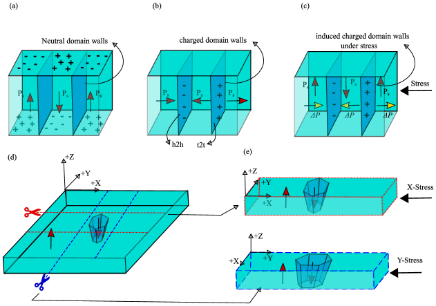
For the last decade, ferroelectric domain walls (DWs) have been in the focus of research due to their outstanding optical, electrical, and topological properties, that promise numerous applications such as resistive switches and non-volatile ferroelectric memory devices [1, 2, 3]. These applications take advantage of conductive nature of ferroelectric DWs, where on and off states of the devices can be defined by the resistance of DWs [2, 4, 5, 6, 7, 8]. In most models, the conductivity of DWs is connected to the order parameter of the surrounding domains, which for ferroelectrics is the spontaneous polarization . In the context of conductivity, three main configurations of a DW are distinguished:
(1) Neutral DWs; when from neighbouring domains are aligned antiparallel to each other as depicted in Fig. 1(a).
(2) head-to-head (h2h) DWs; when from different domains meet at their positive ends; and
(3) tail-to-tail (t2t) DWs; which are the opposing configuration of h2h, see Fig. 1(b).
The convergence of polarization in cases (2) and (3), creates non-zero bound surface charges localized at the DW, which becomes a source of the so-called depolarization field. This field is then compensated by mobile screening charge carriers such as electrons, holes, polarons, or mobile ions. In some cases the depolarization field is even strong enough ( 1 MV/cm) to locally bend the conduction band below the Fermi level, hence creating a 2D electron gas at the DW, which, for example, was reported in BaTiO3 [9, 10]. The presence of such charged CDWs is reported for many ferroelectrics such as BiFeO3 [11, 12], PbTiO3 [13], BaTiO3 [14], HoMnO3 [15], LiNbO3 [16, 17, 18] etc.
In ferroelectrics, DWs can be easily written, erased, moved, or even switched between different states of conductivity. The most common method is by the application of electric fields. Electric fields are able to create or erase DWs via ferroelectric poling. In case of LiNbO3 it further allows to control the amount of charge accumulation, e.g. by controlling the tilt angle of the DW with respect to the polar axis [19, 4, 20]. The control of charge accumulation, or in other words, the conductivity of DWs allows to enlarge the memory window for ferroelectric based memory devices [4]. Another elegant possibility to control and study the accumulation of bound charges is via direct piezoelectricity [21, 22], i.e. by inducing an additional polarization component through stress or strain [see Fig. 1(c)], which so far has only been reported for a few selected materials. For example, Ederer et al. evaluated the effect of epitaxial strain of up to on the spontaneous polarization () for different ferroelectrics [23]. Experimentally, Chen et. al. measured the spontaneous polarization and conductivity of DWs of strained BiFO3 thin films. They reported that strain tuning changes the DW conductivity by several orders of magnitude indicating effects not just due to screening charges but band-bending as well [24]. In the reported experimental or theoretical cases, the application and amount of strain is limited by lattice-mismatched epitaxial growth of thin films on specifically selected substrates and, therefore, cannot be generalized to all ferroelectric materials or crystallographic orientations [25].
To enable the study of strain on the DW conductivity for any bulk ferroelectric, we report the room temperature domain wall conductivity of LiNbO3 under uniaxial stress, by combining a in-situ tunable uniaxial stress cell with scanning probe microscopy. With the help of conductive atomic force microscopy (cAFM), we show the local change of the current distribution in DWs, when stress is applied along different crystallographic directions in LiNbO3. The experimental results are readily explained with our model based on the direct piezoelectric effect in LiNbO3.
For our study, we have chosen the ferroelectric material lithium niobate (5 MgO-doped LiNbO3), where highly CDWs with currents of up to 1 mA at 10 V in 200 m thick crystals have been reported [19, 26]. Recent experiments in LNO have demonstrated that DWs can be switched between conductive and non-conductive states with a memory window of via electric fields in both, thin films and bulk devices [26, 4]. This switching process can be used for fabricating a two-terminal memory device with an extrapolated 80%-lifetime of years [4]. Therefore, LiNbO3 is an ideal model system to study the effects of strain on DW conductivity.
II Results
The samples used in this measurement are single-crystal Z-cut 5% MgO-doped LiNbO3 (LNO). For this study we analyzed two samples, which are prepared such that stress can be applied along different crystal axes [see Fig. 1(d) and (e)]. Sample LNO-01 is compressed along the crystallographic x-axis, while sample LNO-02 is compressed along the crystallographic y-axis. Both these samples carry a conductive hexagonally shaped DW, which was first rendered more conductive (enhanced DWs) using the enhancement procedure by Godau et.al. [19](see method section). The samples were stressed with the help of a uniaxial stress cell, which is based on piezoelectric stacks [27]. This cell can apply controlled, user defined tensile or compressive stress in a continuous fashion on the bulk samples (see method section). Application of the stress along these two directions results in principally different behaviors of the DW conductivity of LiNbO3, as explained in section II.1 by the theoretical model.
II.1 Theoretical model
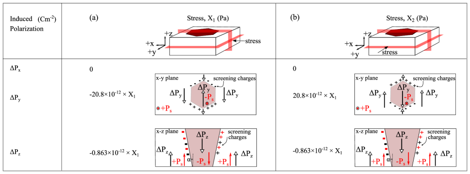
The conductivity of ferroelectric DWs in LiNbO3 is believed to be related to the amount of screening charges present at the DW. As shown in Fig. S2 and S3 of supplement subsection S1.1 and discussed in the literature [19, 18, 26] any increase of the DW inclination angle , with respect to the polar axis results in an increase of the screening charge carrier density and, ideally its conductivity by . Alike, applying stress to the sample results in a change of screening charge carriers by induced polarization through the direct piezoelectric effect. This can be used to predict and describe the behavior of CDWs with respect to applied stress. The polarization in the crystal of LiNbO3 can be described via:
| (1) |
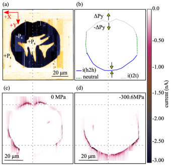
where is the matrix of piezoelectric strain coefficients and is the stress matrix [28, 29, 30] (details on the calculation and the tensor elements for LiNbO3 are presented in the supplement section S2). When the LiNbO3 crystal is stressed along the crystallographic x-axis as in the sample LNO-01 which we have measured in this work, an extra polarization is induced along both the y- and z-axes, as provided in Fig 2(a). The values of induced polarizations along the y-axis ( Cm-2) and the z-axis ( Cm-2) for a compressive stress of -100 MPa are significantly smaller than the spontaneous polarization of LiNbO3 ( 0.7 Cm-2 [31]). However, as the polarization is projected perpendicular to at the DW, it contributes as a cosine component to the surface charge density equation and results in a significant surface charge density () at the DWs ( = 2P +2P), as depicted by the sketches in Fig. 2(a). This is in the same order of magnitude as the natural charge density for small angles of inclination of , typically observed for enhanced domain walls [19]. As a result, x-compressed DWs, which are oriented at some angle to the y-axis, should become h2h or t2t like, and thus should be screened additionally by negative or positive mobile charge carriers, respectively. Depending on their geometry, from now on we will refer to them as induced h2h, i(h2h), and induced t2t, i(t2t) DWs.
Since LiNbO3 is piezoelectric along the y-axis, one should expect exactly the opposite behaviour when the sample is compressed along that crystallographic y-axis, as we will indeed report below for sample LNO-02. This happens due to the sign inversion of in equation 1. This is depicted in Fig. 2(b). In a y-compression scenario, the induced polarization will change the direction by 180∘ in contrast to the in x-compression, and the DWs which were i(h2h) in x-compression will become i(t2t) for y-compression.
When applying this model to our LNO-01 and LNO-02 samples, we expect DW currents to behave as described in the sketches of Fig. 3 (b), (d) and Fig. 5(b). We show that the DWs highlighted in blue-solid lines should become i(h2h) type (negatively screened) while grey dotted DWs should become i(t2t) type (positively screened), and green dashed DWs should not be influenced by uniaxial stress at all. The opposite behaviour should be observed under tensile stress.
II.2 Experiment: domain walls under uniaxial stress
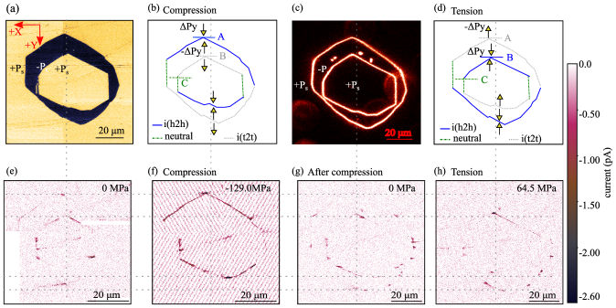
In order to locate the domains, piezo response force microscopy (PFM) was performed on the +z side of sample LNO-01, as illustrated in Fig. 3 (a). As seen in Fig. 3 (c), the PFM image agree well with SHG imaging and confirm the presence of the same DWs. In the PFM image, yellow and black color contrast represents a phase difference of between two different orientations, while in SHG microscopy the presence of DWs is indicated by an enhanced backscattered signal. Based on the PFM scans, cAFM was performed at the same location at different stresses while applying a -10 V dc voltage to the bottom contact (-z side). Fig. 3(e) shows a cAFM overview at 0 MPa. Here, only parts of the DWs show conductivity. The reason for this could be different near surface inclination angles of DWs, leading to locally different Schottky barriers, which has been reported earlier [19, 15, 20, 18]. However, the observed locations correspond to the shape and location of the DWs as observed in PFM and SHG microscopy.
When compressing the sample along the x-axis, we expect the DWs with i(h2h) and i(t2t) configuration to be additionally charged. The i(h2h) DWs must get more conductive because the amount of negative screening charges increases. On the other hand i(t2t) DWs first should fully compensate the preexisting negative screening charges at the DW. This means for i(t2t) DWs that the current should first reduce to zero and on application of further compressive stress, one should expect these i(t2t) DWs to become conductive again. Both types of DWs are highlighted by blue-solid and grey-dotted lines in the sketch in Fig. 3(b). The image in Fig. 3(f) below shows a cAFM scan taken at -129 MPa. Indeed, we see an enhanced conductivity for the i(h2h) configurations, while the i(t2t) walls are observed to show a decreasing conductivity. When the compression is relaxed back to 0 MPa again, as depicted in Fig. 3(g), it retains a qualitatively similar picture to the initial state [Fig. 3(e)]. When tensile stress is applied, only the walls with a i(h2h) configuration with respect to the induced polarization exhibit a significant increased conductivity, while the induced i(t2t) DWs show a disappearing conductivity as shown in Fig. 3(d) and (h). In all cases, the neutral walls with respect to the induced polarization show a similar qualitative and quantitative behavior, independent of the applied stress. Additional experiments were performed in intermediate steps of approximately 16.12 MPa for both, tension and compression in the range from -129 MPa (compression) up to +64.5 MPa (tensile), as well as repeated multiple times. Selected results can be found in Fig. S6 of the supplement subsection S3.1. In all cases, similar qualitative and quantitative results were obtained as expected, where only the i(h2h) DWs show a significant contribution to the conductivity. The observation that only h2h DWs exhibit a high electric conductivity has been reported before for LiNbO3 and other ferroelectrics for tilted DWs, and can be explained by the proposed microscopic mechanism of DW conductivity. For LiNbO3, the DW conductivity is explained by hoping transport of electrons in bound-polaronic states, while hole polarons are expected to be only a weak contributor. Hence, only h2h, i.e. negatively screened walls, will contribute to overall conductivity. In this regard, our experiment is in agreement with the polaron-hopping transport mechanism [32].
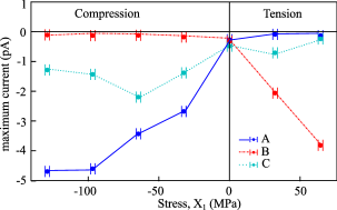
Based on the piezoelectric theory the induced polarization is directly proportional to the applied stress. Hence, the conductivity for h2h walls should increase approximately linear with increasing polarization. In order to show the change in the current as function of stress more clearly, we have plotted in Fig. 4 the maximum current from line profiles A, B and C (taken from i(h2h), i(t2t) and neutral parts of DWs in Fig. 3, respectively). This graph shows three different kinds of behavior:
(1) The DW depicted along the line profile A shows an increase in conductivity on compression, while it shows almost no response for tensile stress within the resolution limit of our setup.
(2) In contrast, the DW in profile B shows the opposite response, as this wall gets an induced i(h2h) configuration for tensile stress. On the other hand,
(3) The DW in line profile C shows no distinctive behavior.
It should be noted that in this experiment additional to the effects of induced polarizations Py and Pz, we also expect to see effects from local roughness and local inclinations of the DWs. Therefore, charge carriers inside the crystal might not move in a simple path vertically along the DWs and therefore distorting the ideally expected linear relationships. Effects like this may be predicted based on a resistor network model of DWs [33] in future work.
Apart from the cAFM studies on the sample LNO-01, we have also investigated the response of the DWs to stress with large, deposited electrodes covering all the DWs. These electrodes were the same that were also used for the enhancement procedure. In this macroscopic picture, we see an overall increase in conductivity with applied stress similar to Fig. 4, line profile A for LNO-01. This is in agreement with the fact that in this specific sample the i(h2h) DWs dominate the conductivity. However, it should be noted that this result may not be generalized to all samples and will depend on which induced domain type dominates [i(h2h) or i(t2t)] the conductivity, as was observed for sample LNO-02(details to macroscopic curve for both samples are provided in Fig. S2 and S3 of the supplement section S1.1). Therefore, this retrospectively motivates the microscopic cAFM study.
For a sample compressed along y-axis different behaviour to x-axis compression according to the model is expected. Hence, when the similar cAFM measurement was performed on sample LNO-02, we observed the opposite response as was explained by the theoretical model in last section. Fig. 5(a) represents the PFM image taken on +z surface. The DWs in sample LNO-02 are more conductive by factor of 3 even at 0 MPa, as compared to sample LNO-01 as shown by Fig. 5(c). This is due to the inclination angle of DWs in LNO-02 is more than in LNO-01 by 1∘, see angle calculation in Fig S4 and S5 of supplement subsection S1.2. We only show the cAFM image of the outer wall in sample LNO-02 because of the irregular shape of the inner DW. Nevertheless, when compressive stress of -300.6 MPa was applied along the y-axis, the walls along the +y direction of the crystal becomes i(h2h) and hence more conductive which is opposite to the response of sample LNO-01 as shown by in Fig. 5(d).
(Further information on sample LNO-02 can be found in the supplement).
III Methods
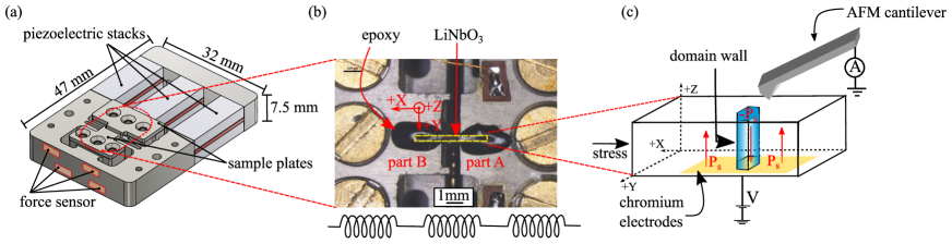
III.1 Stress cell
The stress cell used in this work has a central piezoelectric stack, connected to the main body of the cell, which applies compressive stress, while the outer stacks apply tensile stress [27], see Fig. 6(a). Mechanically, the cell is composed of two different parts A and B of different spring constants which are then connected by the sample in mechanical series, as shown in Fig. 6(b). Being in series, all parts along with the sample experience the same force but different stresses. This force on the cell is measured by a force sensor placed at the end of device, which consists of four strain gauges mounted in a Wheatstone bridge configuration. The cell is controlled by a feedback loop written in Python.
III.2 Sample preparation
The single crystal, single domain of 5 MgO-doped LiNbO3 used in this work were obatined from “Yamaju Ceramics Co., Ltd.”. The domains in the crystal were subsequently written by the UV-assited poling method [34]. The samples were later cut to narrow bars, see Fig. 1(e), such that the sample LNO-01 and LNO-02 have the cross sections of 310 m 200 m (z y) and 370 m 200 m (z x), respectively. Afterwards fabricated domain structures were treated to increase the conductivity by the procedure developed by Godau et al. [19]. In the enhancement procedure chromium electrodes were used to apply the -500V DC voltage to 200 m thick LiNbO3 crystal. With this the DWs moved and the inclination angle of DWs increased by 1∘ [35], hence the current increased by a factor of 104 (at -10V) compared to as-poled DWs (see Fig. S2, S3 of supplement and section on angle calculation).
III.3 Scanning force microscopy(PFM and cAFM)
The measurements were performed on a NX10 scanning probe microscope from “Park Systems Corp.”. PFM [36] on the samples was performed using pure platinum tips model RMN-25PT300B (free resonance frequency, 20 kHz) as a top contact, while applying the external mechanical stress. For PFM, an alternating voltage of 20 Vp-p at a frequency smaller than contact resonance frequency ( 41 kHz) was applied to the cantilever.
Conductive atomic force microscopy (cAFM) was also performed using the same RMN tips. The sample in this case was kept at -10V while the cantilever and the stress cell were kept at ground, see Fig. 6(c).
IV Conclusion
In summary, we demonstrate that uniaxial compressive or tensile stress along the x and y- axes can be used to purposely tune the conductivity of ferroelectric DWs in LiNbO3. Here, applying uniaxial stress to a sample results in a change of screening charges on the domain boundary due to the piezoelectric effect. Depending on the relative orientations of the stress and the DW respectively, a DW can deliberately be configured h2h or t2t, for example. Based on this, our results show that the conductivity is approximately proportional to the amount of induced negative screening charges, i.e. i(h2h) configurations, while induced positively charged walls, i.e. i(t2t) configurations, show a rapid decrease in overall conductivity down to bulk conductivity. This observation hints towards electron polarons, rather than hole polarons, that are the main contributor to the conductivity of DWs in LiNbO3 [37]. The same behavior was observed when measurements were repeated many times over a period of two months (see supplement section S3.2). Our measurements were performed on a stress cell that allows us to control uniaxial stress independent of a substrate or temperature and, therefore, offering large flexibility for studying different geometries or materials. In conclusion, with uniaxial stress we can gain a directional control of DW conductivity potentially allowing novel applications such as stress or strain based nanosensors, as well as providing fundamental insights into the properties of DWs.
V Acknowledgments
We express our great gratitude for financial support by the Deutsche Forschungsgemeinschaft (DFG) through joint DFG-ANR project “TOPELEC ”(Nos. EN 434/41-1 and ANR-18-J.CE92-0052-1), the CRC1415 (ID: 417590517), the FOR5044 (ID: 426703838) www.FOR5044.de, as well as by the Würzburg-Dresden Cluster of Excellence on “Complexity and Topology in Quantum Matter”- ct.qmat (EXC 2147; ID: 39085490). We also acknowledge the excellent support by the Light Microscopy Facility, a Core Facility of the CMCB Technology Platform at TU Dresden, where the SHG analysis was performed and Park Systems, on which the cAFM measurements were performed. Furthermore, we thank D. Bieberstein and T. Gemming from IFW Dresden for assistance with dicing of the wafers, Dr. Elke Beyreuther for valuable discussions and Ahmed Samir Lotfy for his lab assistance to this work.
References
- Kirbus et al. [2019a] B. Kirbus, C. Godau, L. Wehmeier, H. Beccard, E. Beyreuther, A. Haußmann, and L. M. Eng, Real-Time 3D Imaging of Nanoscale Ferroelectric Domain Wall Dynamics in Lithium Niobate Single Crystals under Electric Stimuli: Implications for Domain-Wall-Based Nanoelectronic Devices, ACS Applied Nano Materials 2, 5787 (2019a).
- Sharma et al. [2017] P. Sharma, Q. Zhang, D. Sando, C. H. Lei, Y. Liu, J. Li, V. Nagarajan, and J. Seidel, Nonvolatile ferroelectric domain wall memory, Science Advances 3, 1 (2017).
- Zhao et al. [2020] J. Zhao, C. Ma, M. Rüsing, and S. Mookherjea, High Quality Entangled Photon Pair Generation in Periodically Poled Thin-Film Lithium Niobate Waveguides, Physical Review Letters 124, 163603 (2020).
- Kämpfe et al. [2020] T. Kämpfe, B. Wang, A. Haußmann, L.-Q. Chen, and L. M. Eng, Tunable Non-Volatile Memory by Conductive Ferroelectric Domain Walls in Lithium Niobate Thin Films, Crystals 10, 804 (2020).
- Jiang et al. [2018] J. Jiang, Z. L. Bai, Z. H. Chen, L. He, D. W. Zhang, Q. H. Zhang, J. A. Shi, M. H. Park, J. F. Scott, C. S. Hwang, and A. Q. Jiang, Temporary formation of highly conducting domain walls for non-destructive read-out of ferroelectric domain-wall resistance switching memories, Nature Materials 17, 49 (2018).
- Li et al. [2016] L. Li, J. Britson, J. R. Jokisaari, Y. Zhang, C. Adamo, A. Melville, D. G. Schlom, L. Q. Chen, and X. Pan, Giant Resistive Switching via Control of Ferroelectric Charged Domain Walls, Advanced Materials 28, 6574 (2016).
- Gruverman et al. [2008] A. Gruverman, D. Wu, and J. F. Scott, Piezoresponse force microscopy studies of switching behavior of ferroelectric capacitors on a 100-ns time scale, Physical Review Letters 100, 3 (2008).
- Catalan et al. [2012] G. Catalan, J. Seidel, R. Ramesh, and J. F. Scott, Domain wall nanoelectronics, Reviews of Modern Physics 84, 119 (2012).
- Seidel Editor and Walls [2016] J. Seidel Editor and D. Walls, Topological Structures in Ferroic Materials, edited by J. Seidel, Springer Series in Materials Science, Vol. 228 (Springer International Publishing, Cham, 2016) pp. 103–138.
- Sluka et al. [2012] T. Sluka, A. K. Tagantsev, D. Damjanovic, M. Gureev, and N. Setter, Enhanced electromechanical response of ferroelectrics due to charged domain walls, Nature Communications 3, 748 (2012).
- Condurache et al. [2021] O. Condurache, G. Dražić, N. Sakamoto, T. Rojac, and A. Benčan, Atomically resolved structure of step-like uncharged and charged domain walls in polycrystalline BiFeO 3, Journal of Applied Physics 129, 054102 (2021).
- Rojac et al. [2017] T. Rojac, A. Bencan, G. Drazic, N. Sakamoto, H. Ursic, B. Jancar, G. Tavcar, M. Makarovic, J. Walker, B. Malic, and D. Damjanovic, Domain-wall conduction in ferroelectric BiFeO 3 controlled by accumulation of charged defects, Nature Materials 16, 322 (2017).
- Stolichnov et al. [2015] I. Stolichnov, L. Feigl, L. J. McGilly, T. Sluka, X.-K. Wei, E. Colla, A. Crassous, K. Shapovalov, P. Yudin, A. K. Tagantsev, and N. Setter, Bent Ferroelectric Domain Walls as Reconfigurable Metallic-Like Channels, Nano Letters 15, 8049 (2015).
- Sluka et al. [2013] T. Sluka, A. K. Tagantsev, P. Bednyakov, and N. Setter, Free-electron gas at charged domain walls in insulating BaTiO3, Nature Communications 4, 1806 (2013).
- Wu et al. [2012] W. Wu, Y. Horibe, N. Lee, S.-W. Cheong, and J. R. Guest, Conduction of Topologically Protected Charged Ferroelectric Domain Walls, Physical Review Letters 108, 077203 (2012).
- Gonnissen et al. [2016] J. Gonnissen, D. Batuk, G. F. Nataf, L. Jones, A. M. Abakumov, S. Van Aert, D. Schryvers, and E. K. H. Salje, Direct Observation of Ferroelectric Domain Walls in LiNbO 3 : Wall-Meanders, Kinks, and Local Electric Charges, Advanced Functional Materials 26, 7599 (2016).
- Werner et al. [2017] C. S. Werner, S. J. Herr, K. Buse, B. Sturman, E. Soergel, C. Razzaghi, and I. Breunig, Large and accessible conductivity of charged domain walls in lithium niobate, Scientific Reports 7, 9862 (2017).
- Schröder et al. [2012] M. Schröder, A. Haußmann, A. Thiessen, E. Soergel, T. Woike, and L. M. Eng, Conducting Domain Walls in Lithium Niobate Single Crystals, Advanced Functional Materials 22, 3936 (2012).
- Godau et al. [2017] C. Godau, T. Kämpfe, A. Thiessen, L. M. Eng, and A. Haußmann, Enhancing the Domain Wall Conductivity in Lithium Niobate Single Crystals, ACS Nano 11, 4816 (2017).
- Lu et al. [2019] H. Lu, Y. Tan, J. P. V. McConville, Z. Ahmadi, B. Wang, M. Conroy, K. Moore, U. Bangert, J. E. Shield, L. Chen, J. M. Gregg, and A. Gruverman, Electrical Tunability of Domain Wall Conductivity in LiNbO 3 Thin Films, Advanced Materials 31, 1902890 (2019).
- Chen et al. [2012] Z. Chen, X. Zou, W. Ren, L. You, C. Huang, Y. Yang, P. Yang, J. Wang, T. Sritharan, L. Bellaiche, and L. Chen, Study of strain effect on in-plane polarization in epitaxial BiFeO 3 thin films using planar electrodes, Physical Review B - Condensed Matter and Materials Physics 86, 1 (2012).
- Alsubaie et al. [2017] A. Alsubaie, P. Sharma, G. Liu, V. Nagarajan, and J. Seidel, Mechanical stress-induced switching kinetics of ferroelectric thin films at the nanoscale, Nanotechnology 28, 10.1088/1361-6528/aa536d (2017).
- Ederer and Spaldin [2005] C. Ederer and N. A. Spaldin, Effect of epitaxial strain on the spontaneous polarization of thin film ferroelectrics, Physical Review Letters 95, 2 (2005), arXiv:0508005 [cond-mat] .
- Chen et al. [2018] D. Chen, Z. Bai, Y. Zhang, and A. Jiang, Strain induced enhancement of erasable domain wall current in epitaxial BiFeO 3 thin films, Journal of Applied Physics 124, 194102 (2018).
- Schlom et al. [2007] D. G. Schlom, L.-Q. Chen, C.-B. Eom, K. M. Rabe, S. K. Streiffer, and J.-M. Triscone, Strain Tuning of Ferroelectric Thin Films, Annual Review of Materials Research 37, 589 (2007).
- Kirbus et al. [2019b] B. Kirbus, C. Godau, L. Wehmeier, H. Beccard, E. Beyreuther, A. Haußmann, and L. M. Eng, Real-Time 3D Imaging of Nanoscale Ferroelectric Domain Wall Dynamics in Lithium Niobate Single Crystals under Electric Stimuli: Implications for Domain-Wall-Based Nanoelectronic Devices, ACS Applied Nano Materials 2, 5787 (2019b).
- Hicks et al. [2014] C. W. Hicks, M. E. Barber, S. D. Edkins, D. O. Brodsky, and A. P. Mackenzie, Piezoelectric-based apparatus for strain tuning, Review of Scientific Instruments 85, 065003 (2014).
- Yamada et al. [1967] T. Yamada, N. Niizeki, and H. Toyoda, Piezoelectric and Elastic Properties of Lithium Niobate Single Crystals, Japanese Journal of Applied Physics 6, 151 (1967).
- Smith and Welsh [1971] R. T. Smith and F. S. Welsh, Temperature Dependence of the Elastic, Piezoelectric, and Dielectric Constants of Lithium Tantalate and Lithium Niobate, Journal of Applied Physics 42, 2219 (1971).
- Weis and Gaylord [1985] R. S. Weis and T. K. Gaylord, Lithium niobate: Summary of physical properties and crystal structure, Applied Physics A Solids and Surfaces 37, 191 (1985).
- Wemple et al. [1968] S. H. Wemple, M. DiDomenico, and I. Camlibel, Relationship between linear and quadratic electrooptic coefficients in LiNbO3, LiTiO3, and other oxygen octahedra ferroelectrics based on direct measurement of spontaneous polarization, Applied Physics Letters 12, 209 (1968).
- Xiao et al. [2018] S. Y. Xiao, T. Kämpfe, Y. M. Jin, A. Haußmann, X. M. Lu, and L. M. Eng, Dipole-Tunneling Model from Asymmetric Domain-Wall Conductivity in LiNb O3 Single Crystals, Physical Review Applied 10, 1 (2018).
- Wolba et al. [2018] B. Wolba, J. Seidel, C. Cazorla, C. Godau, A. Haußmann, and L. M. Eng, Resistor Network Modeling of Conductive Domain Walls in Lithium Niobate, Advanced Electronic Materials 4, 1700242 (2018).
- Müller et al. [2003] M. Müller, E. Soergel, and K. Buse, Influence of ultraviolet illumination on the poling characteristics of lithium niobate crystals, Applied Physics Letters 83, 1824 (2003).
- Kämpfe et al. [2014] T. Kämpfe, P. Reichenbach, M. Schröder, A. Haußmann, L. M. Eng, T. Woike, and E. Soergel, Optical three-dimensional profiling of charged domain walls in ferroelectrics by Cherenkov second-harmonic generation, Physical Review B 89, 035314 (2014).
- Soergel [2011] E. Soergel, Piezoresponse force microscopy (PFM), Journal of Physics D: Applied Physics 44, 464003 (2011).
- Eliseev et al. [2011] E. A. Eliseev, A. N. Morozovska, G. S. Svechnikov, V. Gopalan, and V. Y. Shur, Static conductivity of charged domain walls in uniaxial ferroelectric semiconductors, Physical Review B - Condensed Matter and Materials Physics 83, 1 (2011).