Chemical Strain Engineering of MAPbI3 Perovskite Films
Abstract
This study introduces a new chemical method for controlling the strain in methylammonium lead iodide (MAPbI3) perovskite crystals by varying the ratio of Pb(Ac)2 and PbCl2 in the precursor solution. To observe the effect on crystal strain, a combination of piezoresponse force microscopy (PFM) and X-ray diffraction (XRD) is used. The PFM images show an increase in the average size of ferroelastic twin domains upon increasing the PbCl2 content, indicating an increase in crystal strain. The XRD spectra support this observation with strong crystal twinning features that appear in the spectra. This behaviour is caused by a strain gradient during the crystallization due to different evaporation rates of methylammonium acetate and methylammonium chloride as revealed by time-of-flight secondary ion mass spectroscopy (ToF-SIMS) and grazing incidince x-ray diffraction (GIXRD) measurements. Additional time-resolved photoluminescence (TRPL) show an increased carrier lifetime in the MAPbI3 films prepared with higher PbCl2 content, suggesting a decreased trap density in films with larger twin domain structures. The results demonstrate the potential of chemical strain engineering as an easy method for controlling strain-related effects in lead halide perovskites.
1 Introduction
Hybrid lead halide perovskites [1, 2, 3, 4, 5, 6] show remarkable properties such as a direct adjustable band gap [7, 8, 9], high defect tolerance [10], and long charge carrier lifetimes [11, 12, 13] that make them ideally suited as absorber materials for photovoltaic applications. An interesting effect that has been observed in many hybrid lead halide perovskite materials is that the optoelectronic properties can be strongly influenced by external or internal strain. Thus, strain engineering can be a useful method to control and tune the optoelectronic properties or structural stability of perovskite materials[14, 15]. For example, Zhu et al. showed improved charge extraction at the perovskite-hole transport layer interface by eliminating the strain gradient, flattening the valence band[16]. Kim et. al. used strain engineering to relax the crystal lattice of formamidinium lead iodide (FAPbI3), enabling improved solar cell performance[17]. In addition, strain engineering had also been used by various groups to increase the stability of perovskite structures. Zhao et al. showed strain engineering of MAPbI3 by mechanichally bending the substrate increased the stability[18]. Strain engineering was also used to stabilize meta-stable phases such as CsPbI3 and FAPbI3 by introduction of biaxial strain via cooling a perovskite crystal clamped to a ceramic substrate [19] or applying strain by heteroepitaxially growing the perovskite on another perovskite material [20].
Another important strain-related effect observed in methylammonium lead iodide (MAPbI3) crystals is the formation of sub-granular ferroelastic twin domains. Ferroelastic twin domains in tetragonal MAPbI3 were first observed via piezoresponse force microscopy (PFM) by our group [21], followed by many others[22, 23, 24, 25]. The domains form due to the strain resulting from the cubic to tetragonal phase change at 57°C. Strelcov et al. observed via polarized optical microscopy (POM) that mechanical stress leads to a rearrangement of the twin domains in MAPbI3, supporting the conclusion that the domains are ferroelastic [26]. Since our first report in 2016, ferroelastic twins have been observed by many other techniques, including transmission electron microscopy (TEM) [24], X-ray diffraction (XRD)[27], and neutron scattering[28].
The existence of a sub-granular domain structure raises the question whether these domains have an influence on the electronic transport properties. Recently, Xiao et al. [29] concluded from PL and lifetime mapping experiments that the ferroelastic twin domains are benign to recombination kinetics. To separate potential grain boundary effects, our group recently investigated large isolated MAPbI3 grains. Using time-resolved PL microscopy, we found an anisotropic charge transport that was correlated to the ferroelastic twin domain structure in the crystal [30]. In particular, the charge diffusion perpendicular to the ferroelastic domains was slower compared to the charge diffusion parallel to the domains.
Such an anisotropic diffusion would be interesting for guiding charge carriers, e.g. to the electrodes of an optoelectronic device. Thus, a targeted manipulation or engineering of the twin domain structure would be desirable. Next to domain manipulation through mechanical straining[26], we showed that the ferroelastic twin domains structure changes when using different cooling rates after annealing [30, 31]. Here, a slower cooling rate resulted in a more dense and ordered domain structure whereas a higher cooling rate lead to disordered and less dense twin domains. Lastly, Röhm et al. demonstrated the domain manipulation via a lateral electric field [32]. However, all the domain manipulation methods mentioned above are not easy to scale up for mass production.
In this study, we introduce a new method for controlling the mechanical strain during the crystal growth via the composition of the precursor solution. In particular, we use different ratios of Pb(Ac)2 and PbCl2 to synthesize MAPbI3 thin films on glass substrates in order to adjust the overall crystallization of MAPbI3 films. Acetate and chloride anions were chosen because they require similar annealing temperatures for evaporation/sublimation. Using a combination of PFM and XRD, we observed an increase in crystal strain connected to an increase in the average twin domain size upon increasing the PbCl2 content. Additionally, we observed a change from stripe-like to rectangular domains, an effect that has been connected to increased crystal strain[26]. Based on time-of-flight secondary ion mass spectroscopy (ToF-SIMS) experiments where we found an accumulation of chloride at the substrate interface, we suggest that the strain during crystal growth is caused by the combined effect of low temperature crystallization and ion exchange during annealing. This chloride accumulation is most likely caused by different evaporation rate of the methylammonium acetate and sublimation rate of methylammonium chloride. Additional time-resolved photoluminescence (TRPL) showed an increased carrier lifetime in the MAPbI3 films prepared with higher PbCl2 content, suggesting a decreased trap density in films with larger twin domain structures.
2 Results and Discussion
2.1 Piezoresponse Force Microscopy (PFM)
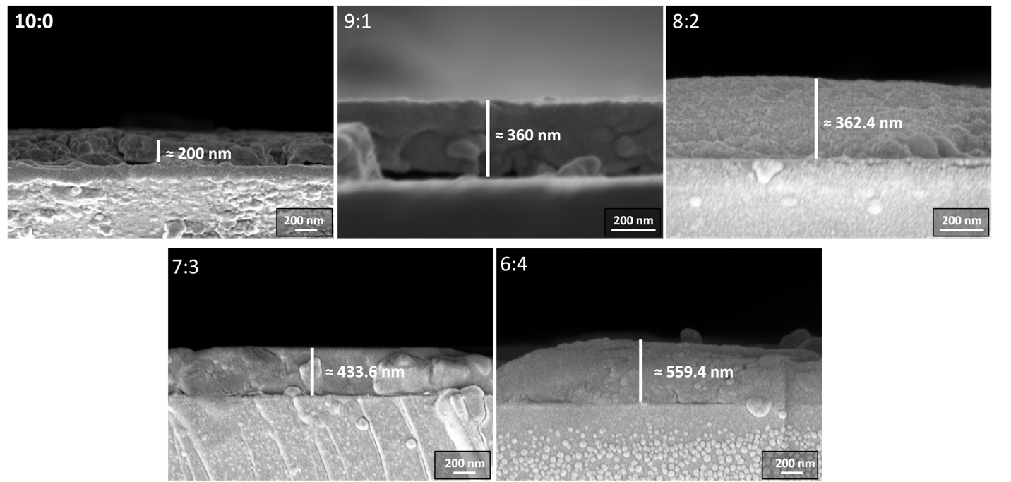
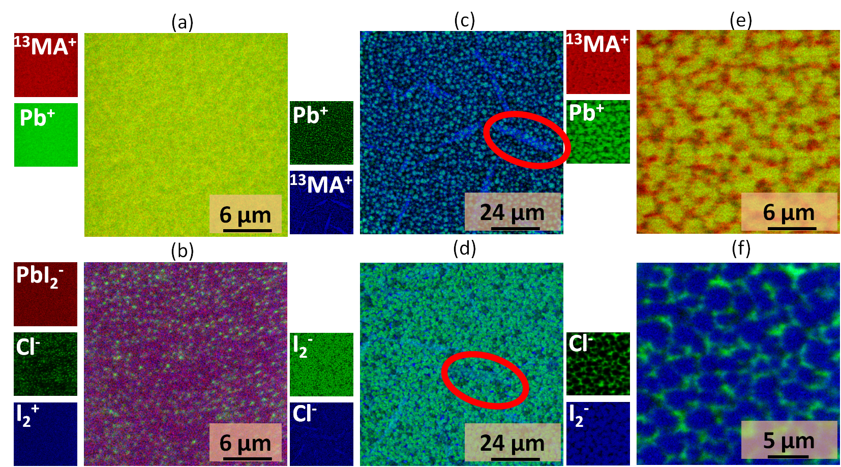
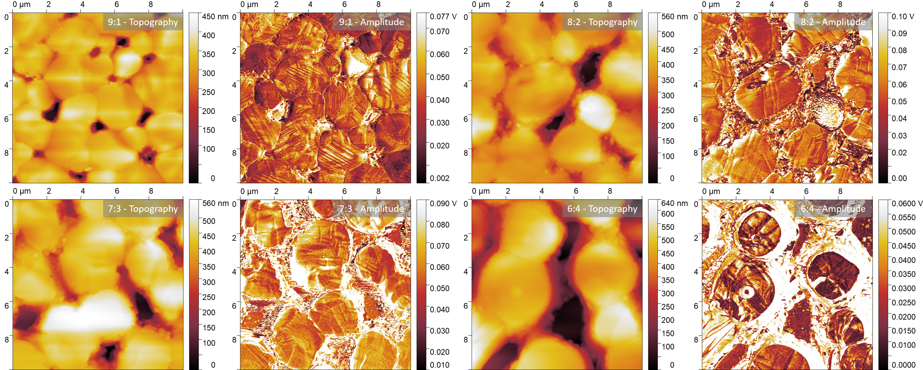
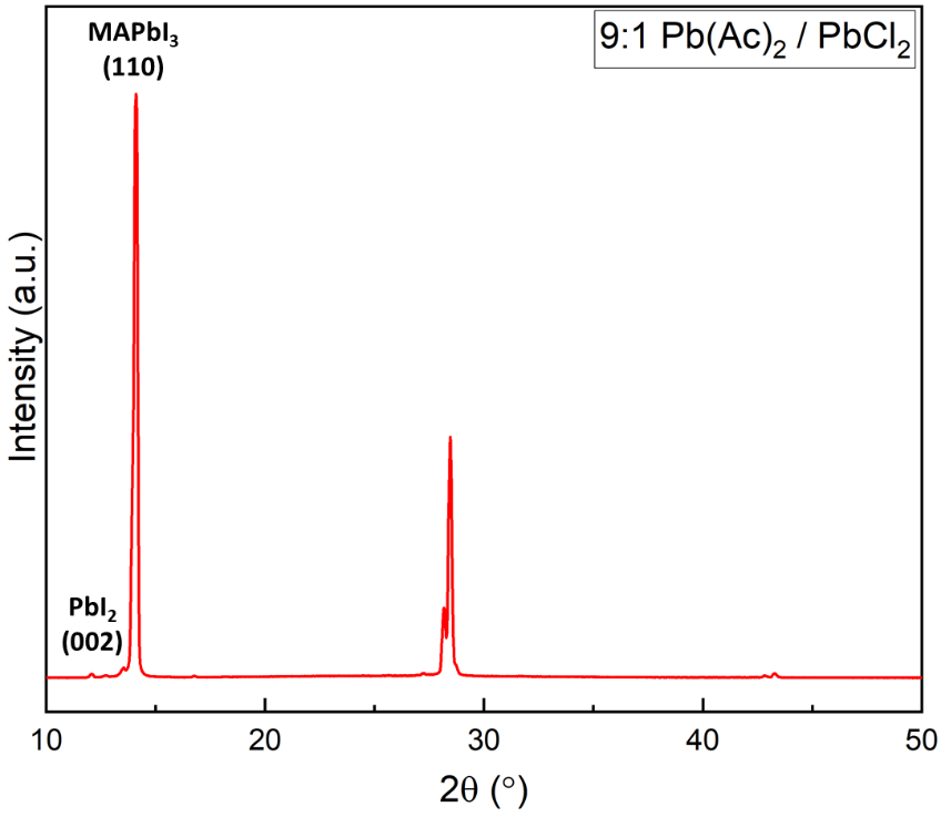
We prepared several batches of MAPbI3 films on glass with precuror ratios between 9:1 and 6:4 and investigated the topography and the lateral piezoresponse using AFM/PFM (Figure 1a-d and S2, details on the working mechanism of PFM are given in the methods section). Figure 1e shows the average grain sizes obtained from several areas of the films with changing Pb(Ac)2 / PbCl2 ratios. The most obvious effect of the the precursor ratio change is an increase in average grain size (d) from 2.04±0.11 µm for the 9:1 Pb(Ac)2 / PbCl2 ratio to 3.9±0.3 µm for the 6:4 Pb(Ac)2 / PbCl2 ratio (Figure 1e). A MAPbI3 film prepared from pure Pb(Ac)2 precursor had an even smaller average grain size of 0.85±0.31 µm (Figure S1, Supporting Information). The decrease in grain size upon lowering the PbCl2 content comes from the decreased Cl or MACl amount which speeds up the crystallization of perovskite and leads to smaller grains[33]. Furthermore, the combined effect of MACl and DMF annealing seems to be causing a significant increase in grain size compared to MAPbI3 film prepared from pure Pb(Ac)2 precursor. In addition to the grain size, the general grain morphology also changed upon decreasing Pb(Ac)2 / PbCl2 ratio. In between the perovskite grains we observed more pinholes and undefined structures (Figure 1b). On average, the density of pinholes and undefined structures increases with decreasing Pb(Ac)2 / PbCl2 ratio (Figure S2, Supporting Information), suggesting these structures could be caused by residual PbI2 or MAPbCl3 that forms after the spin coating [27]. The reason for this effect could again be a slower crystallization in the MAPbI3 film due to the lower volatility of MACl compared to MA(Ac). Later on, we will show that this interpretation is also supported by ToF-SIMS (Figure 3),UV-Vis absorption (Figure S11, Supporting Information), and XRD reflection results (Figure 2).
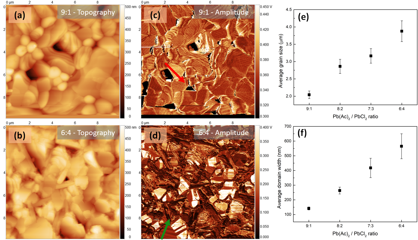
The lateral PFM amplitude images show the familiar striped ferroelastic domain structure [21] (Figure 1c and d). Compared to MAPbI3 films with 9:1 Pb(Ac)2 / PbCl2 ratio (Figure 1c), films prepared from the 6:4 precursor ratio show a less dense domain structure (Figure 1d). In particular, we observed an increase in the width of the ferroelastic twin domains with increasing PbCl2 content. Figure 1f shows average ferroelastic twin domain width values gathered from various areas of the samples. The distances between the high amplitude and low amplitude areas revealed an average domain widths (w) of 137.5±10 nm for the MAPbI3 film with 9:1 and 558.33±90 nm and 6:4 Pb(Ac)2 / PbCl2 ratio, respectively (Figure 1f).
As twin domains are purely strain related, it seems obvious from the changing domain pattern that the strain in the films is influenced by different Pb(Ac)2 / PbCl2 ratios. The work by Strelcov et al. [26] has demonstrated that external stress can alter the domain structure. Their results show that upon increasing the strain within the MAPbI3 films the stripe-shaped domains evolve into larger areas. Furthermore, the emergence of non-90°domain angles were observed upon increased external stress[26]. We also observed such domain shapes (Figure 1), suggesting that the precursor mixing with Pb(Ac)2 / PbCl2 or MA(Ac) and MACl increases the strain within the Pb(Ac)2 / PbCl2 structure.
2.2 X-Ray Diffraction
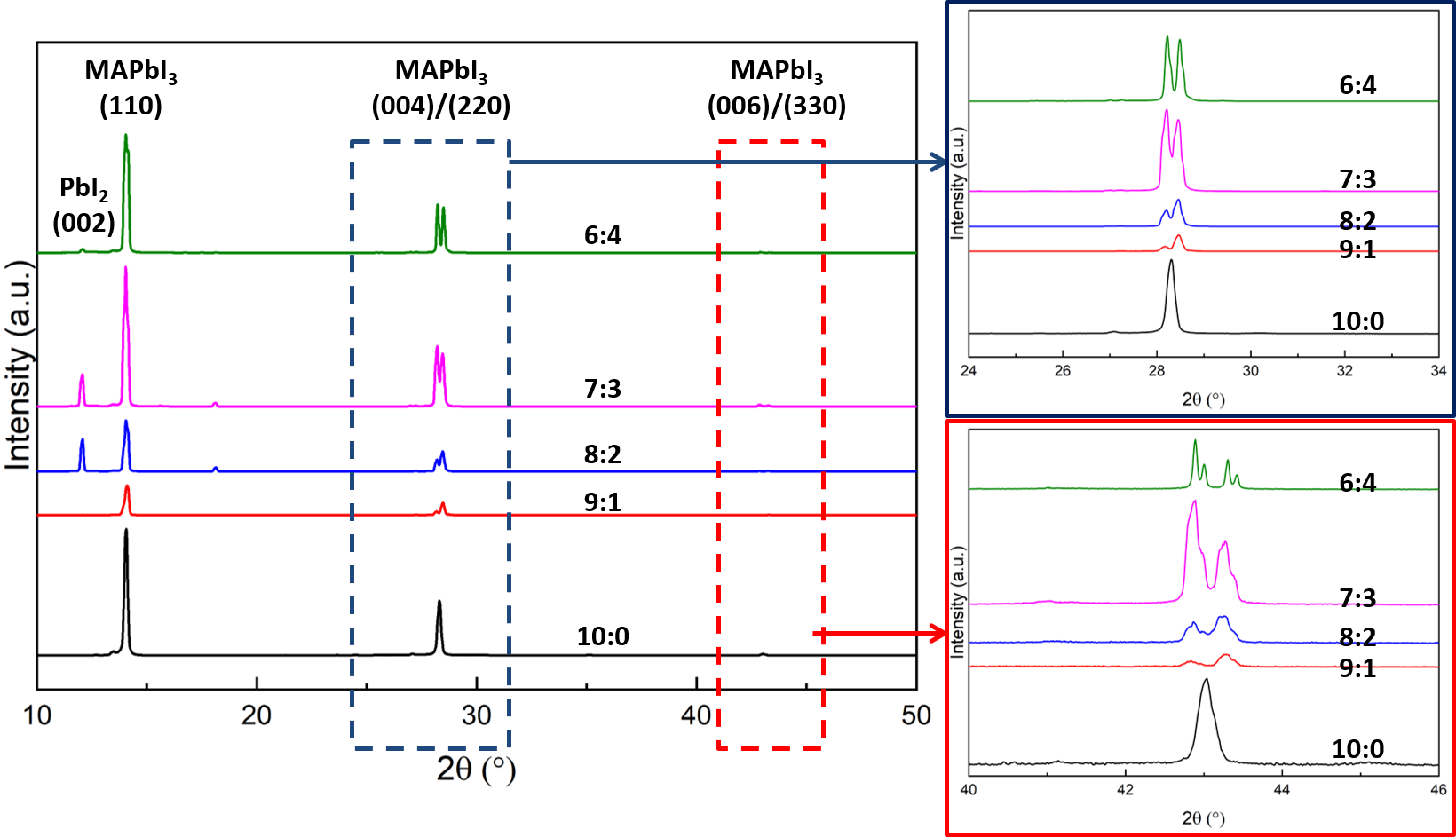
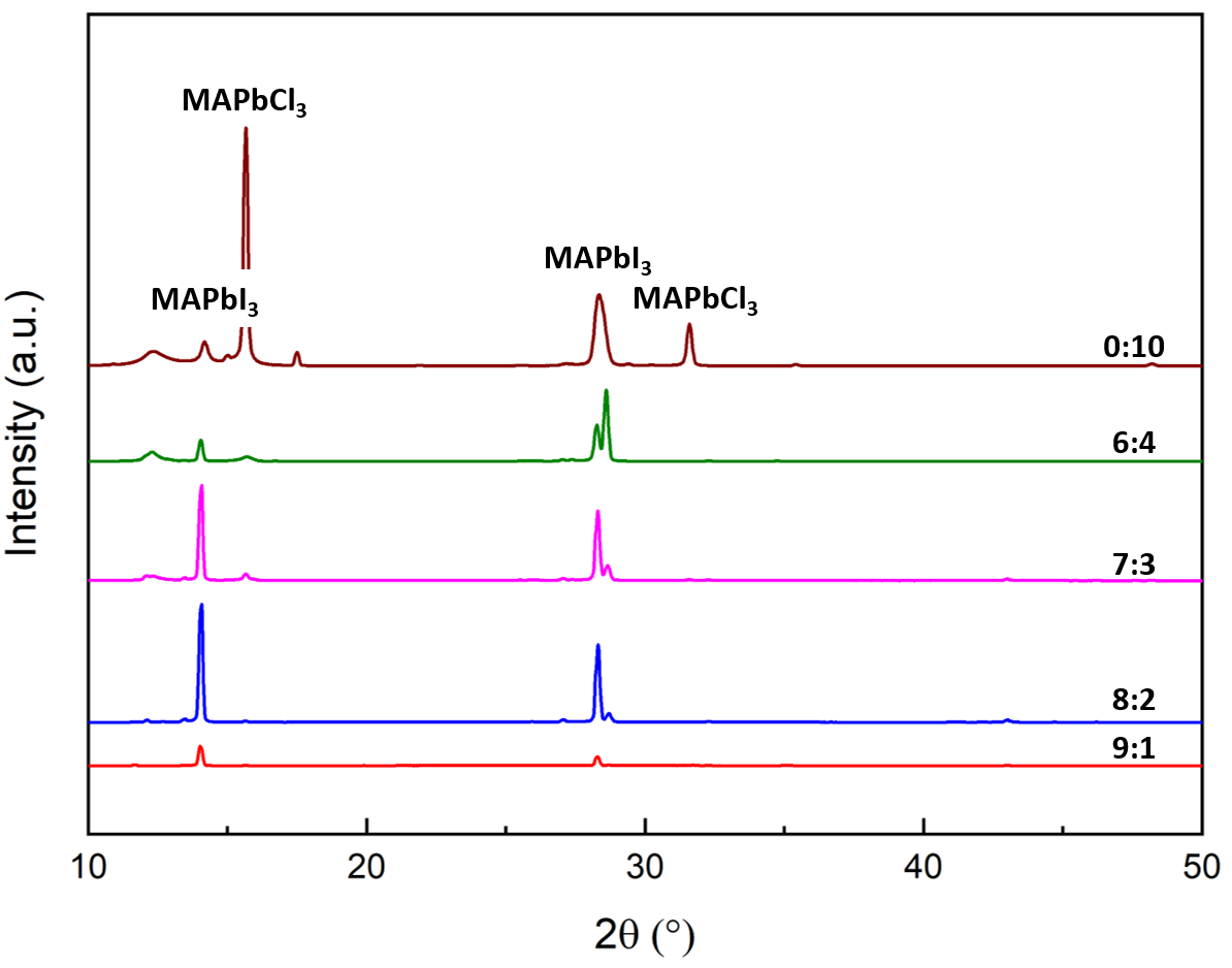
To support the hypothesis of precursor-induced strain adjustment in our MAPbI3 films with different Pb(Ac)2 / PbCl2 ratios, we performed X-ray diffraction (XRD) measurements. In the XRD, all mixed precursor samples showed the typical reflections for MAPbI3 with addition of PbI2 (Figure 2 and S3) and some unidentified weak peaks around 18° that may belong to intermediates or a Lewis acid-base adduct due to retarded crystallization caused by increased PbCl2 [34]. The MAPbI3 (110) / PbI2 (002) intensity ratio reaches to a maximum to some degree PbI2 (002) peak is quenched by MAPbI3 (110) intensity. We also observed a peak splitting around 28° due to {00l}/{hk0} twinning in MAPbI3 films [27] (Figure 2, blue box) in MAPbI3 films with Pb(Ac)2 / PbCl2. The intensity ratio of the (004) peaks to the (220) peaks around 28° increased when the Pb(Ac)2 / PbCl2 ratio was decreased. The lower inset of Figure 2 (red box) shows the XRD signal in the range between 40 and 46°. Again, as the Pb(Ac)2 / PbCl2 ratio was decreased, the (006)/(330) peak intensity ratios increased. Interestingly, we found a further splitting of the split peaks in samples prepared from a 6:4 Pb(Ac)2 / PbCl2 ratio, resulting in four peaks around 43°. Based on the work by Dang et al. [35], these additional peaks may belong to the (134) and (402) planes. Such further peak splitting in the XRD could be related to lower symmetry for smaller Pb(Ac)2 / PbCl2 ratios as a result from the formation of non-90° domains. A similar observation in XRD pattern of MAPbI3 was observed by Leonhard et al.[36] where the emerging peaks disappear upon further annealing, indicating strain relaxation. These results suggest that the larger domain areas in the PFM images in Figure 1(b) belong to {00l} facets and that their XRD intensity increases due to increased area. Furthermore, the observation of a second peak splitting may indicate an increased residual stress resulted by different Pb(Ac)2 / PbCl2.
To learn more about the homogeneous strain behaviour within the MAPbI3 films, we analyzed the XRD peak shifts as a function of Pb(Ac)2 / PbCl2 ratio. The position for MAPbI3 (110) peak for 10:0, 9:1, 8:2, 7:3, and 6:4 Pb(Ac)2 / PbCl2 ratios were observed at around 14°. One important observation in MAPbI3 (110) plane for 6:4 Pb(Ac)2 / PbCl2 ratio is the emerging shoulder at 14.14° (Figure 2). This splitting of the (110) plane suggests that another twinning starts to take place in these samples, likely caused by a higher strain. The peak splitting trends of (004)/(220) and (006)/(330) suggest that the peak at the higher scattering angles would belong to {hk0} planes where the peak at the lower scattering angles would belong to the {00l} planes, possibly (002). Furthermore, the positions of split MAPbI3 (004)/(220) peaks were observed at 28.32° (only (220)), 28.18/28.47°, 28.2/28.46°, 28.21/28.45°, and 28.23/28.49° for 10:0, 9:1, 8:2, 7:3, and 6:4 Pb(Ac)2 / PbCl2 ratios, respectively. It is safe to assume that strain controls the trends observed in the XRD measurements since the enlarged domains were also observed in PFM as a result of increased strain. Here, a shift to lower scattering angles in MAPbI3 (110) plane for Pb(Ac)2 / PbCl2 ratios lower than 9:1 which may indicate the emergence of another peak from the (002) plane. Alternatively, this shift may indicate lattice expansion based on the Bragg’s law and interplanar distance formulas (Equation S1 and S2, Supporting Information). Moreover, a shift to the higher scattering angles for MAPbI3 (004) plane and a shift to lower scattering angles for MAPbI3 (220) was observed with decreasing Pb(Ac)2 / PbCl2 ratio which may indicate lattice shrinking and lattice expansion, respectively (Equation S1 and S2, Supporting Information).
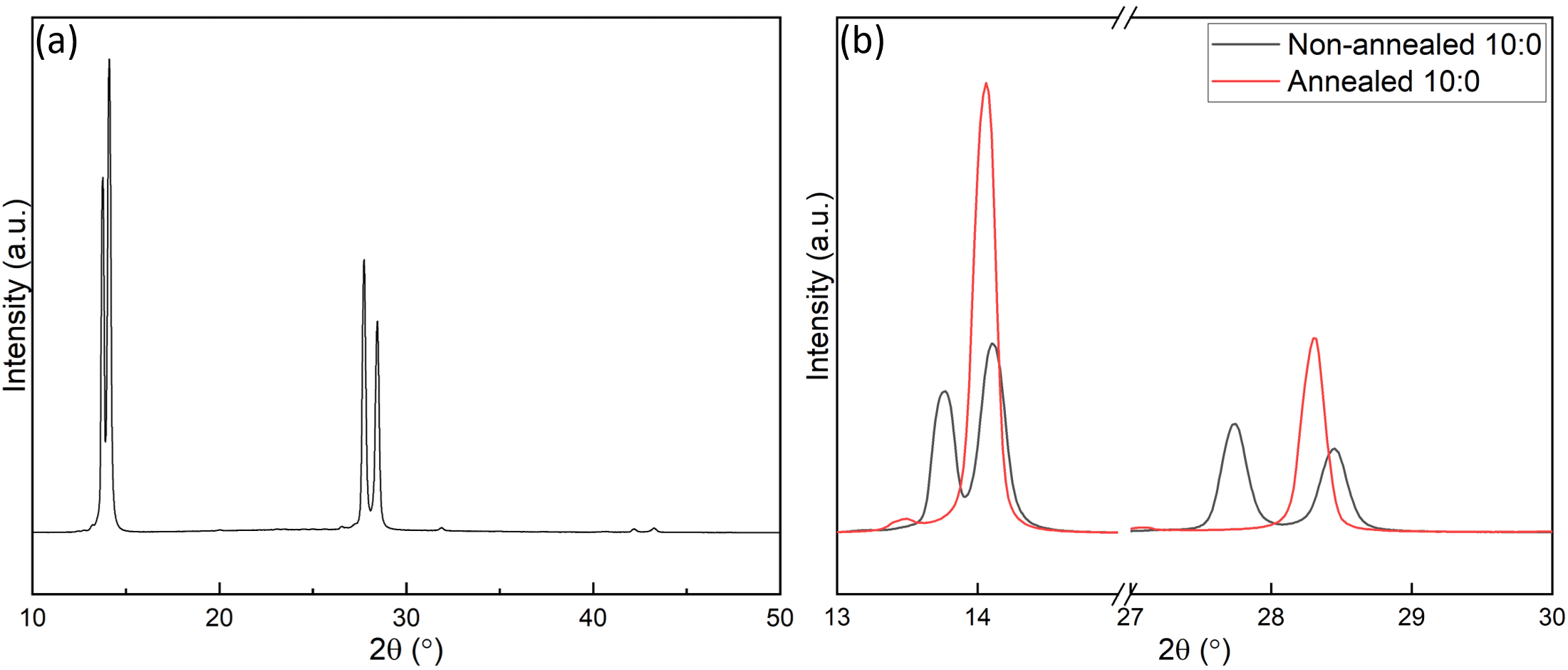
Lastly, we have also performed an XRD measurement on a MAPbI3 film made from a precursor solution containing only MAI and Pb(Ac)2. This sample in particular was not annealed but only dried at room temperature in the glovebox since MA(Ac) is much more volatile compared to MACl and MAPbI3 can form without any heat treatment. The resulting films had a very small grain structure, which made PFM experiments impossible. Therefore, the twinning was only monitored via XRD for this sample (Figure S4a, Supporting Information). The resulting XRD pattern exhibited larger peak splitting, even more distinct then MAPbI3 with 6:4 Pb(Ac)2 / PbCl2 ratio. This result supports the notion of room temperature twinning in MAPbI3 [28]. Also, the stronger (004) signal in non-annealed MAPbI3 film made from only MAI and Pb(Ac)2 compared to annealed samples in Figure 2 is because of strain relaxation upon annealing.
2.3 Chemical Gradients and Strain Mechanism
To synthesize the MAPbI3, methylammonium iodide (MAI), lead acetate (Pb(Ac)2), and lead chloride (PbCl2) precursors were utilized. In this synthesis, the molar ratio of MA precursor to Pb precursor is 3:1 as can given in Eq (1):
3 MAI + PbX_2 -¿ MAPbI_3 + 2MAX
where X can be Ac, Cl, or I. The MAX compound is volatile and evaporates during the annealing of the film. The volatility and thus the evaporation rate of MAX depends on the X anion used in the precursor solution. Therefore, the crystallization kinetics in the MAPbI3 film is controlled by the evaporation rate of the MAX compound.
The observed changes in the ferroelastic twin domain structure in PFM and the peak splitting behaviour in the XRD spectra suggest a correlation between the strain in the MAPbI3 films and the Pb(Ac)2 / PbCl2 ratio in the precursor solution. A recent study by Medjahed et al. [27] has investigated the strain in MAPbI3 films prepared from a 3MAI/PbCl2 solution by monitoring the twinning via XRD. According to this study, MAPbCl3 forms within the film prior to annealing and I- / Cl- ion exchange occurs during annealing. This process gives rise to strain formation within the MAPbI3 film and eventually results in twin formation.
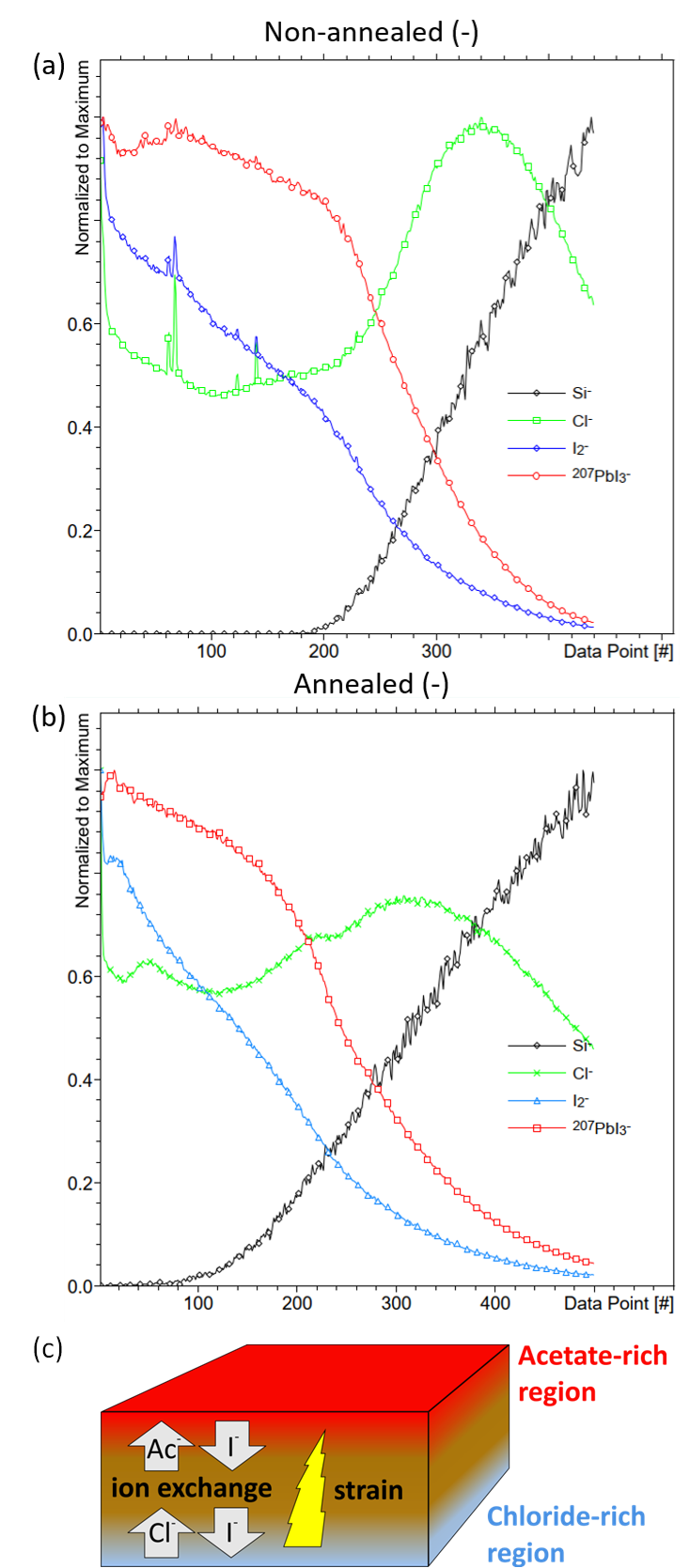
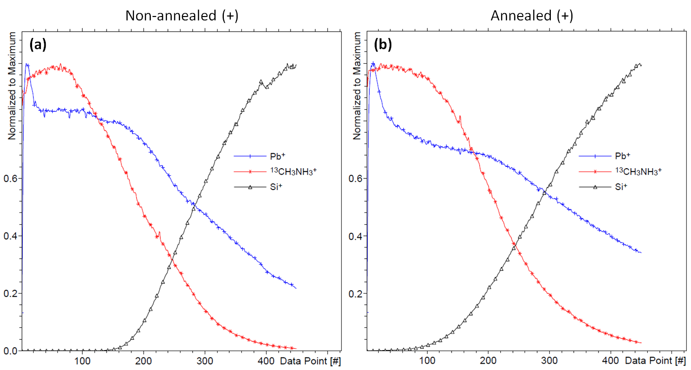
To investigate chemical kinetics within the perovskite film, we carried out ToF-SIMS. The profiles for both PbI and Cl- show a pronounced chemical gradient within the film (Figure 3a and b). In the non-annealed film, we observed elevated levels of Cl- at the bottom of the film compared to static/central part of the profile line. As suggested previously, there might be volatile compounds on the surface involving Cl- which could be the reason for high Cl- amount on the surface. High Cl- amount in the depths of the film on the other hand shows that Cl- ions tend to localize closer to the substrate in the mixed precursor MAPbI3 film as they do in pure MAI/PbCl2 films [37]. A similar trend was also observed for Cl- in the annealed MAPbI3 film as well, however with an increased uniformity through the film. This can be an indication of I- / Cl- ion exchange that leads to the formation of MAPbI3.
The depth profiles in both pristine and annealed MAPbI3 films show I and PbI signals with the opposite trend of Cl-. After the precursor deposition, MAPbI3 grains form closer to the surface while Cl-rich species stay at the bottom of the film. Upon annealing, MACl reaches the surface through the ion exchange. This ion exchange reaction of MAPbCl3 is expected give rise to a vertical strain gradient. An illustration of this vertical ion exchange reaction is given in Figure 3c.
The depth profiles for positive ions (Figure S7) show a uniform Pb+ ion distribution and a slight gradient in MA+ ion distribution. The non-uniform distribution of MA+ ion could also be contributing to the vertical strain gradient as observed before[38].
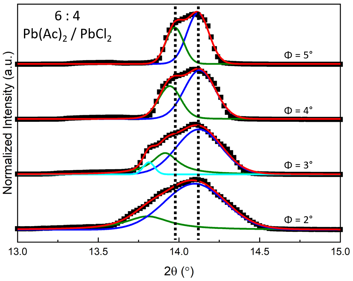
To investigate a potential strain gradient along the vertical direction of the film, we employed grazing incidence x-ray diffraction (GIXRD). GIXRD enables to change the x-ray penetration into the film by changing the incidence angle, providing depth-dependent crystal structure information. The GIXRD spectra of a MAPbI3 film with 6:4 Pb(Ac)2 / PbCl2 ratio shows a change in XRD reflection around 14°(Figure S6, Supporting Information). Deconvolution of the signal reveals a clear shift in the lattice parameters as the x-ray penetration into the perovskite film changes. These shifts are a clear signature of a vertical strain gradient.
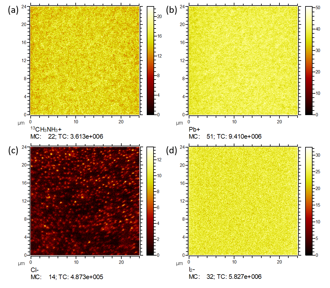
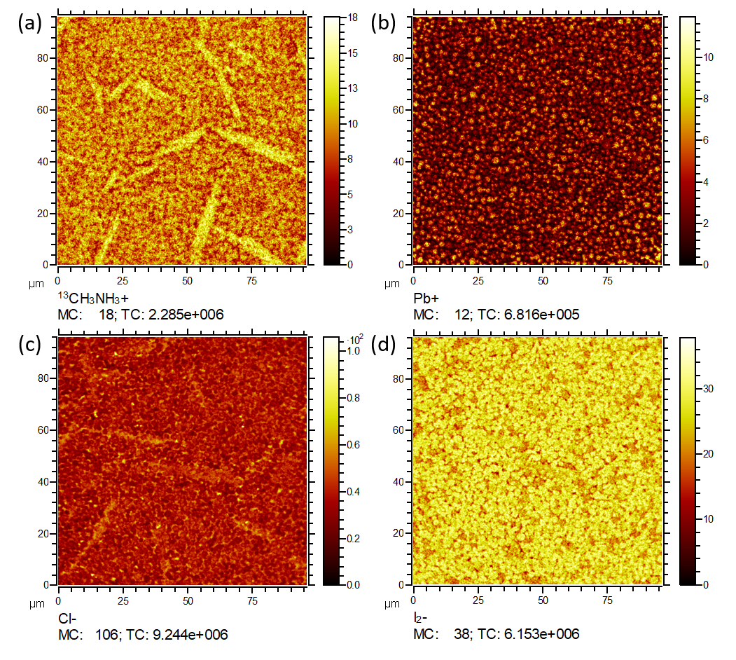
The lateral chemical distribution was also determined using ToF-SIMS on non-annealed and annealed MAPbI3 films with 6:4 Pb(Ac)2 / PbCl2 ratio (Figure 4). The ion distribution in non-annealed MAPbI3 film reveals uniform distribution of MA+, Pb+, and I ions after spin coating whereas Cl- ions show a distribution pattern (Figure 4a and b). Based on the information we obtained from XRD measurements on non-annealed samples (Figure S5, Supporting Information), perovskite films at this stage should be consisting of MAPbI3 and MAPbCl3. Therefore, we suggest the Cl-rich areas in the film are mostly MAPbCl3 areas where the acetate-rich areas quickly transform into MAPbI3. Upon annealing, some morphological and chemical changes occured within the perovskite film: MA- and Cl-rich needle-like structures are prominent in the ToF-SIMS images (blue images in Figure 4c and d, marked with red), similar to the needle structures that we observed in the AFM images (Figure 1 b). In contrast, the Pb+ distribution was much more homogeneous (Figure 4c), whereas the I concentration was reduced in the needle-like structures (Figure 4d), suggesting these structures could be MACl that forms after I- / Cl- ion exchange. At larger magnification, (Figure 4e and d), we see that grain interiors are rich in MA+, Pb+, and I, whereas the exterior of the grains are rich in Cl-. However, there are small areas where the MA+ and Pb+ maps do not exactly match. These map mismatches suggest that the structures outside of MAPbI3 grains could be belonging to structures such as PbI2 and MACl that is not sublimated yet. In addition, we observed small amounts of Cl- inside of the MAPbI3 grains, suggesting a minor Cl- doping could be taking place during fabrication. The ion maps show that next to a vertical chemical gradient there is also a lateral chemical gradient within the perovskite films (Figure 3). Since the correlation between the vertical chemical gradient and the strain gradient in the perovskite film is well established through our GIXRD results (Figure S6, Supporting Information) and supported by other studies [27, 38], we conclude that lateral strain will be present within the films, as well.
2.4 Optical Measurements
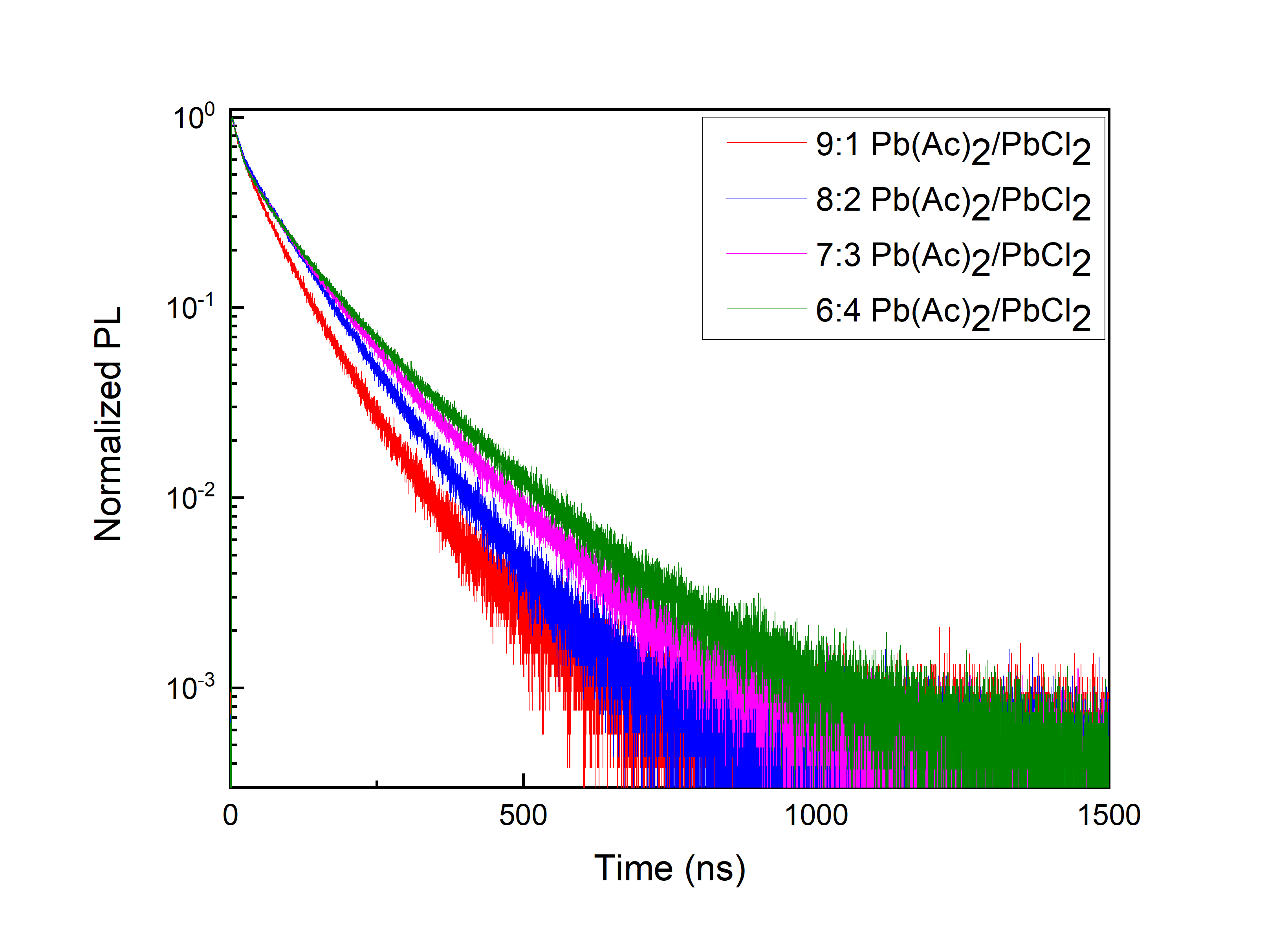
Ferroelastic domain walls distort the local crystalline order and might form energetic barriers [30, 39]. In our earlier study, we found an alternating polarization at the domain walls that could act as shallow traps states or scattering centres, affecting the charge carrier dynamics [30]. To study the effect of different domain morphologies on charge carrier lifetimes, we conducted time-resolved photoluminescence (TRPL) measurements on our MAPbI3 film with different Pb(Ac)2 / PbCl2 ratios (Figure 5). We fitted the results bi-exponentially to obtain lifetime parameters. We found that the carrier lifetime increased from 68.47 ns for the film with 9:1 ratio to 104.35 ns for the 6:4 Pb(Ac)2 / PbCl2 ratio (all values are given in Table S1). This trend suggests the charged carriers move more freely in case of lower Pb(Ac)2 / PbCl2 ratios where the density of ferroelastic domain walls is decreased since the low energy barriers caused by the domain walls are eliminated. This result is in an agreement with our previous findings and previously proposed energetic barriers theory. Furthermore Zhang et al. discovered that the charge carrier mobility in MAPbI3 is plane dependent i.e. anisotropic[40] which also offers an explanation for the energy barriers caused by ferroelastic twin domains.
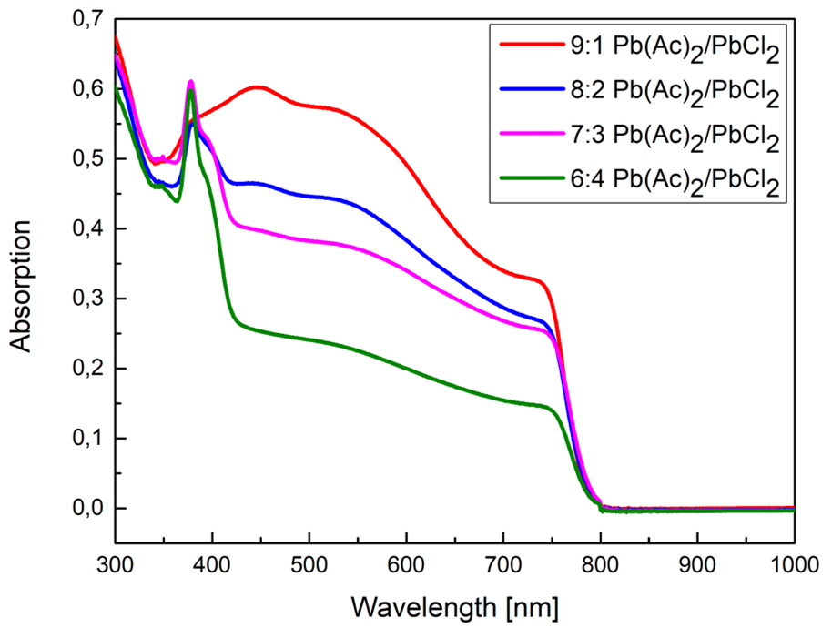
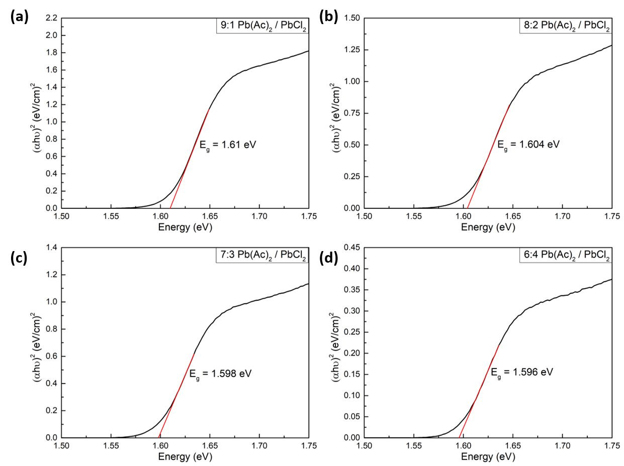
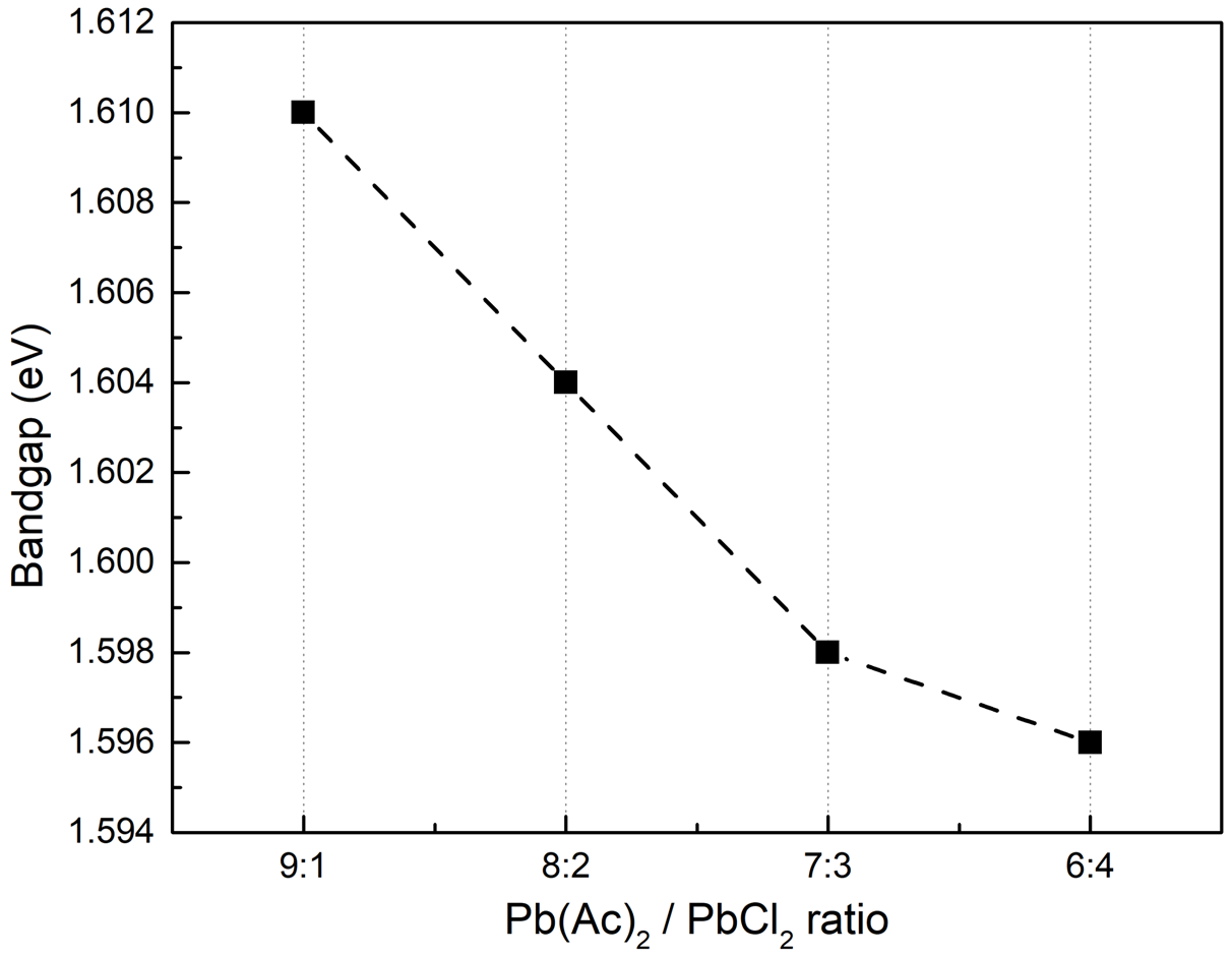
To monitor the presence of additional phases and the optical properties, we performed UV-Vis spectroscopy on the MAPbI3 films with all the different Pb(Ac)2 / PbCl2 ratios (Figure S11). All samples showed an absorption band edge around 780 nm, suggesting that the bandgap of MAPbI3 did not change as a result of different precursor ratios. The absorption edge around 600 nm that is visible in all spectra comes from PbI2 which is in an agreement with the PbI2 signal that we observed in XRD measurements. Furthermore, at any Pb(Ac)2 / PbCl2 ratio below 8:2 a new peak at 390 nm emerged belonging to MAPbCl3. This matches with the expectation since MAPbCl3 forms when PbCl2 is used or increased in the precursor solution [27], which was also supported by ToF-SIMS results (Figure 3) and non-annealed XRD results (S5, Supporting Information). Furthermore, the absorption decreased with decreasing Pb(Ac)2 / PbCl2 ratio due to decreasing amount of MAPbI3 in the obtained film. This is possibly a result of the slow crystallization of MAPbI3 due to the presence of PbCl2. Nevertheless, the MAPbCl3 phase could not be detected by the XRD measurements in Figure 2, most likely due to the low MAPbCl3 content in the films. In addition, we calculated Tauc plots (Figure S12, Supporting Information) from the absorption data from UV-vis results (Figure S11, Supporting Information). The band gap of MAPbI3 films slightly decreased with decreasing Pb(Ac)2 / PbCl2 ratio (Figure S13, Supporting Information). Since the bandgap of MAPbI3 is the same for (110) and (001) planes [40], the bandgap change can be attributed to increased strain as suggested elsewhere[16].
3 Conclusion
In this work we have shown a chemical route to control the strain in MAPbI3 thin films by using different Pb(Ac)2 / PbCl2 ratios in the precursor solution. Using PFM and XRD, we monitored the internal structure, in particular the formation of ferroelastic twin domains - a clear signature of internal strain. The PFM results showed an increase in the average ferroelastic twin domain areas as the Pb(Ac)2 / PbCl2 ratio decreased. The XRD results confirmed that this increase was accompanied by an increase in lattice strain. We suggest that this strain increase is caused by the volatility difference of MA(Ac) and MACl which eventually leads to crystallization rate differences in various regions in the film. This difference leads to room temperature formation of highly strained MAPbI3 in MA(Ac) areas and I- / Cl- exchange occurs in Cl-rich areas resulting in increased strain with increased PbCl2 amount. The chemical gradient and depending strain gradient were observed via ToF-SIMS and XRD measurements, respectively. To observe the effect of the resulting ferroelastic twin domain configurations on the charge carrier dynamics, we conducted TRPL measurements. The presence of larger ferroelastic twin domain areas i.e. fewer domain walls resulted in longer charge carrier lifetimes, supporting our earlier hypothesis of shallow energy barriers at twin domain walls[30].
Our work shows that the crystal strain and thereby the formation of ferroelastic twin domains can be chemically manipulated by simply changing the ratio of different precursors without the need to apply any external force. This strategy offers a simple and scalable route to achieve a favorable domain arrangement in MAPbI3-based devices, enabling faster and more efficient charge extraction. Even beyond domain engineering in MAPbI3, chemical strain engineering is a promising idea for strain engineering in many other other lead halide perovskite materials.
4 Experimental Section
4.1 Materials
Methylalmmonium iodide (MAI) was purchased from Greatcell Energy. Lead acetate (Pb(Ac)2 for perovskite precursor, 98.0 % purity) and lead chloride (PbCl2, 99.999 %) were purchased from Tokyo Chemical Industry and Sigma Aldrich, respectively. Anhydrous dimethylformamide (DMF) was purchased from Sigma Aldrich.
4.2 Perovskite Film Preparation
Glass substrates were brushed with Hellmanex on both sides and washed with hot tap water and milliQ water followed by drying with an air gun. The cleaned substrates were subjected to UV-Ozone treatment (FHR UVOH 150 LAB, 250 W) for 30 minutes with oxygen feeding rate of 1 L/ min right before spin coating.
Two precursor solutions were prepared for the film preparation. Precursor solution 1 was prepared with MAI (477.0 mg, 3 mol), Pb(Ac)2 (325.3 mg, 1 mol), and DMF (1 mL) while precursor solution 2 was prepared with MAI (238.5 mg, 1.5 mol), PbCl2 (137.0 mg, 0.5 mol), and DMF (500 µL). The precursor solutions 1 and 2 were mixed in 9:1, 8:2, 7:3, and 6:4 volume ratios before the fabrication. The perovskite film fabrication was carried out by static spin coating, which was performed at 4000 rpms (1000 rpm/s) for 1 minute after smearing 100 µL solution over the substrate. After the spin coating, all the samples were dried at room temperature for 10 minutes. After drying, all samples were annealed in DMF vapour atmosphere at 100 °C for 10 minutes. Glass petri dishes were used to obtain the DMF vapour atmosphere. The DMF vapour media were prepared before the coating started. The films first put on hotplate outside of the petri dish until it turns black ( 3 seconds) then put under DMF vapour atmosphere. Number of samples per petri dish can be changed from 1 to 4. However, the amount of DMF should be changed accordingly. 15 µL DMF per film was used for the annealing process. All processes were carried out in a nitrogen glovebox.
4.3 Piezoresponse Force Microscopy Measurements
Piezoresponse force microscopy (PFM) is an Atomic force microscopy (AFM) mode, which is used to detect electromechanical material properties on the nanometer scale. A conductive tip is used to detect the response of the sample to an AC voltage.
Lateral piezoresponse force microscopy (PFM) measurements were performed on an Asylum Research MFP-3D AFM from Oxford Instruments and a Zürich Instruments HF2 lock-in amplifier in an argon filled glovebox (O2 and H2O 1ppm). The measurements were carried out with platinum-iridium coated SCM PIT-V2 cantilevers from Bruker with a nominal resonance frequency of 70 kHz and a spring constant of around 2.5 nN nm-1. The measurement of the PFM signal was performed at an AC excitation voltage with a peak amplitude of 2 V at the lateral contact resonance at around 700 kHz to take advantage of the resonance enhancement.
4.4 X-ray Diffraction Measurements
X-ray diffraction (XRD) patterns were taken with Rigaku SmartLab using Cu K radiation. Diffractograms had been recorded in “”- “” geometry, using a Göbel mirror and automatic sample alignment. The scanning rate was 2°/min in steps of 0.01°. The total beam exposure time was 30 minutes.
4.5 Time of Flight Secondary Ion Mass Spectroscopy
ToF-SIMS experiments were performed using a TOF.SIMS5 (NCS) instrument (IONTOF GmbH, Münster, Germany) with 30 keV Bi3 primary ions and 5 keV Ar1500 cluster ions for sputtering at a 45° angle. Surface imaging was facilitated using the ultimate imaging mode at a current of 0.05 pA at a cycle time of 100 µs. Dual beam depth profiling was conducted on an analysis area of 200 × 200 µm2 with a sputter area of 500 x 500 µm2 at a sputter current of 2.5 nA.
4.6 Optical Measurements
Absorption data was collected using a Cary5000 UV-vis-NIR spectrometer by Agilent equipped with an integrating sphere. Time-resolved photoluminescence was conducted via time-correlated single photon counting on a FluoTime300 spectrometer by PicoQuant at an emission wavelength of 770nm, following pulsed 485nm excitation at a repetition rate of 500kHz.
Acknowledgements
Y.Y. and S.A.L.W. acknowledge the SPP2196 project (Deutsche Forschungsgemeinschaft) for funding. K.A.-W. acknowledges support from the Carl-Zeiss-Stiftung.
References
- [1] Akihiro Kojima, Kenjiro Teshima, Yasuo Shirai, and Tsutomu Miyasaka. Organometal halide perovskites as visible-light sensitizers for photovoltaic cells. Journal of the American Chemical Society, 131(17):6050–6051, 2009.
- [2] Michael M Lee, Joël Teuscher, Tsutomu Miyasaka, Takurou N Murakami, and Henry J Snaith. Efficient hybrid solar cells based on meso-superstructured organometal halide perovskites. Science, 338(6107):643–647, 2012.
- [3] Hui-Seon Kim, Chang-Ryul Lee, Jeong-Hyeok Im, Ki-Beom Lee, Thomas Moehl, Arianna Marchioro, Soo-Jin Moon, Robin Humphry-Baker, Jun-Ho Yum, Jacques E Moser, et al. Lead iodide perovskite sensitized all-solid-state submicron thin film mesoscopic solar cell with efficiency exceeding 9%. Scientific reports, 2(1):1–7, 2012.
- [4] Jason J Yoo, Sarah Wieghold, Melany C Sponseller, Matthew R Chua, Sophie N Bertram, Noor Titan Putri Hartono, Jason S Tresback, Eric C Hansen, Juan-Pablo Correa-Baena, Vladimir Bulović, et al. An interface stabilized perovskite solar cell with high stabilized efficiency and low voltage loss. Energy & Environmental Science, 12(7):2192–2199, 2019.
- [5] Oscar A Jaramillo-Quintero, Rafael S Sanchez, Marina Rincon, and Ivan Mora-Sero. Bright visible-infrared light emitting diodes based on hybrid halide perovskite with spiro-ometad as a hole-injecting layer. The journal of physical chemistry letters, 6(10):1883–1890, 2015.
- [6] AZ Ashar, N Ganesh, and KS Narayan. Sensors: Hybrid perovskite-based position-sensitive detectors (adv. electron. mater. 2/2018). Advanced Electronic Materials, 4(2):1870012, 2018.
- [7] Loredana Protesescu, Sergii Yakunin, Maryna I Bodnarchuk, Franziska Krieg, Riccarda Caputo, Christopher H Hendon, Ruo Xi Yang, Aron Walsh, and Maksym V Kovalenko. Nanocrystals of cesium lead halide perovskites (cspbx3, x= cl, br, and i): novel optoelectronic materials showing bright emission with wide color gamut. Nano letters, 15(6):3692–3696, 2015.
- [8] Constantinos C Stoumpos, Christos D Malliakas, and Mercouri G Kanatzidis. Semiconducting tin and lead iodide perovskites with organic cations: phase transitions, high mobilities, and near-infrared photoluminescent properties. Inorganic chemistry, 52(15):9019–9038, 2013.
- [9] T Jesper Jacobsson, Juan-Pablo Correa-Baena, Meysam Pazoki, Michael Saliba, Kurt Schenk, Michael Grätzel, and Anders Hagfeldt. Exploration of the compositional space for mixed lead halogen perovskites for high efficiency solar cells. Energy & Environmental Science, 9(5):1706–1724, 2016.
- [10] K Xerxes Steirer, Philip Schulz, Glenn Teeter, Vladan Stevanovic, Mengjin Yang, Kai Zhu, and Joseph J Berry. Defect tolerance in methylammonium lead triiodide perovskite. ACS Energy Letters, 1(2):360–366, 2016.
- [11] Michael B Johnston and Laura M Herz. Hybrid perovskites for photovoltaics: charge-carrier recombination, diffusion, and radiative efficiencies. Accounts of chemical research, 49(1):146–154, 2016.
- [12] Samuel D Stranks, Giles E Eperon, Giulia Grancini, Christopher Menelaou, Marcelo JP Alcocer, Tomas Leijtens, Laura M Herz, Annamaria Petrozza, and Henry J Snaith. Electron-hole diffusion lengths exceeding 1 micrometer in an organometal trihalide perovskite absorber. Science, 342(6156):341–344, 2013.
- [13] Dong Shi, Valerio Adinolfi, Riccardo Comin, Mingjian Yuan, Erkki Alarousu, Andrei Buin, Yin Chen, Sjoerd Hoogland, Alexander Rothenberger, Khabiboulakh Katsiev, et al. Low trap-state density and long carrier diffusion in organolead trihalide perovskite single crystals. Science, 347(6221):519–522, 2015.
- [14] Erin G Moloney, Vishal Yeddu, and Makhsud I Saidaminov. Strain engineering in halide perovskites. ACS Materials Letters, 2(11):1495–1508, 2020.
- [15] Hurriyet Yuce, Carlo AR Perini, Juanita Hidalgo, Andrés-Felipe Castro-Méndez, Caria Evans, Pablo Franco Betancur, Jacob N Vagott, Yu An, Kathryn Bairley, Mustafa M Demir, et al. Understanding the impact of sri2 additive on the properties of sn-based halide perovskites. Optical Materials, page 111806, 2021.
- [16] Cheng Zhu, Xiuxiu Niu, Yuhao Fu, Nengxu Li, Chen Hu, Yihua Chen, Xin He, Guangren Na, Pengfei Liu, Huachao Zai, et al. Strain engineering in perovskite solar cells and its impacts on carrier dynamics. Nature communications, 10(1):1–11, 2019.
- [17] Gwisu Kim, Hanul Min, Kyoung Su Lee, Do Yoon Lee, So Me Yoon, and Sang Il Seok. Impact of strain relaxation on performance of -formamidinium lead iodide perovskite solar cells. Science, 370(6512):108–112, 2020.
- [18] Jingjing Zhao, Yehao Deng, Haotong Wei, Xiaopeng Zheng, Zhenhua Yu, Yuchuan Shao, Jeffrey E Shield, and Jinsong Huang. Strained hybrid perovskite thin films and their impact on the intrinsic stability of perovskite solar cells. Science advances, 3(11):eaao5616, 2017.
- [19] Julian A Steele, Handong Jin, Iurii Dovgaliuk, Robert F Berger, Tom Braeckevelt, Haifeng Yuan, Cristina Martin, Eduardo Solano, Kurt Lejaeghere, Sven MJ Rogge, et al. Thermal unequilibrium of strained black cspbi3 thin films. Science, 365(6454):679–684, 2019.
- [20] Yimu Chen, Yusheng Lei, Yuheng Li, Yugang Yu, Jinze Cai, Ming-Hui Chiu, Rahul Rao, Yue Gu, Chunfeng Wang, Woojin Choi, et al. Strain engineering and epitaxial stabilization of halide perovskites. Nature, 577(7789):209–215, 2020.
- [21] Ilka M Hermes, Simon A Bretschneider, Victor W Bergmann, Dan Li, Alexander Klasen, Julian Mars, Wolfgang Tremel, Frédéric Laquai, Hans-Jürgen Butt, Markus Mezger, et al. Ferroelastic fingerprints in methylammonium lead iodide perovskite. The Journal of Physical Chemistry C, 120(10):5724–5731, 2016.
- [22] Boyuan Huang, Guoli Kong, Ehsan Nasr Esfahani, Shulin Chen, Qian Li, Junxi Yu, Ningan Xu, Ying Zhang, Shuhong Xie, Haidan Wen, et al. Ferroic domains regulate photocurrent in single-crystalline ch 3 nh 3 pbi 3 films self-grown on fto/tio 2 substrate. npj Quantum Materials, 3(1):1–8, 2018.
- [23] Holger Röhm, Tobias Leonhard, Michael J Hoffmann, and Alexander Colsmann. Ferroelectric domains in methylammonium lead iodide perovskite thin-films. Energy & Environmental Science, 10(4):950–955, 2017.
- [24] Mathias Uller Rothmann, Wei Li, Ye Zhu, Udo Bach, Leone Spiccia, Joanne Etheridge, and Yi-Bing Cheng. Direct observation of intrinsic twin domains in tetragonal ch 3 nh 3 pbi 3. Nature communications, 8(1):1–8, 2017.
- [25] Yongtao Liu, Liam Collins, Roger Proksch, Songkil Kim, Brianna R Watson, Benjamin Doughty, Tessa R Calhoun, Mahshid Ahmadi, Anton V Ievlev, Stephen Jesse, et al. Chemical nature of ferroelastic twin domains in ch 3 nh 3 pbi 3 perovskite. Nature materials, 17(11):1013–1019, 2018.
- [26] Evgheni Strelcov, Qingfeng Dong, Tao Li, Jungseok Chae, Yuchuan Shao, Yehao Deng, Alexei Gruverman, Jinsong Huang, and Andrea Centrone. Ch3nh3pbi3 perovskites: Ferroelasticity revealed. Science advances, 3(4):e1602165, 2017.
- [27] Asma Aicha Medjahed, Pia Dally, Tao Zhou, Noëlla Lemaitre, David Djurado, Peter Reiss, and Stéphanie Pouget. Unraveling the formation mechanism and ferroelastic behavior of mapbi3 perovskite thin films prepared in the presence of chloride. Chemistry of Materials, 32(8):3346–3357, 2020.
- [28] Joachim Breternitz, Michael Tovar, and Susan Schorr. Twinning in mapbi 3 at room temperature uncovered through laue neutron diffraction. Scientific reports, 10(1):1–8, 2020.
- [29] Xun Xiao, Wenhao Li, Yanjun Fang, Ye Liu, Yuchuan Shao, Shuang Yang, Jingjing Zhao, Xuezeng Dai, Rashid Zia, and Jinsong Huang. Benign ferroelastic twin boundaries in halide perovskites for charge carrier transport and recombination. Nature communications, 11(1):1–7, 2020.
- [30] Ilka M Hermes, Andreas Best, Leonard Winkelmann, Julian Mars, Sarah M Vorpahl, Markus Mezger, Liam Collins, Hans-Jürgen Butt, David S Ginger, Kaloian Koynov, et al. Anisotropic carrier diffusion in single mapbi 3 grains correlates to their twin domains. Energy & Environmental Science, 13(11):4168–4177, 2020.
- [31] Sarah M Vorpahl, Rajiv Giridharagopal, Giles E Eperon, Ilka M Hermes, Stefan AL Weber, and David S Ginger. Orientation of ferroelectric domains and disappearance upon heating methylammonium lead triiodide perovskite from tetragonal to cubic phase. ACS Applied Energy Materials, 1(4):1534–1539, 2018.
- [32] Holger Röhm, Tobias Leonhard, Michael J Hoffmann, and Alexander Colsmann. Ferroelectric poling of methylammonium lead iodide thin films. Advanced Functional Materials, 30(5):1908657, 2020.
- [33] Wei Zhang, Michael Saliba, David T Moore, Sandeep K Pathak, Maximilian T Hörantner, Thomas Stergiopoulos, Samuel D Stranks, Giles E Eperon, Jack A Alexander-Webber, Antonio Abate, et al. Ultrasmooth organic–inorganic perovskite thin-film formation and crystallization for efficient planar heterojunction solar cells. Nature communications, 6(1):1–10, 2015.
- [34] Do-Kyoung Lee, Dong-Nyuk Jeong, Tae Kyu Ahn, and Nam-Gyu Park. Precursor engineering for a large-area perovskite solar cell with¿ 19% efficiency. ACS Energy Letters, 4(10):2393–2401, 2019.
- [35] Yangyang Dang, Yang Liu, Youxuan Sun, Dongsheng Yuan, Xiaolong Liu, Weiqun Lu, Guangfeng Liu, Haibing Xia, and Xutang Tao. Bulk crystal growth of hybrid perovskite material ch 3 nh 3 pbi 3. CrystEngComm, 17(3):665–670, 2015.
- [36] Tobias Leonhard, Holger Röhm, Fabian J Altermann, Michael J Hoffmann, and Alexander Colsmann. Evolution of ferroelectric domains in methylammonium lead iodide and correlation with the performance of perovskite solar cells. Journal of Materials Chemistry A, 9(38):21845–21858, 2021.
- [37] Eva L Unger, Andrea R Bowring, Christopher J Tassone, Vanessa L Pool, Aryeh Gold-Parker, Rongrong Cheacharoen, Kevin H Stone, Eric T Hoke, Michael F Toney, and Michael D McGehee. Chloride in lead chloride-derived organo-metal halides for perovskite-absorber solar cells. Chemistry of Materials, 26(24):7158–7165, 2014.
- [38] Yongtao Liu, Anton V Ievlev, Liam Collins, Alex Belianinov, Jong K Keum, Mahshid Ahmadi, Stephen Jesse, Scott T Retterer, Kai Xiao, Jingsong Huang, et al. Strain–chemical gradient and polarization in metal halide perovskites. Advanced Electronic Materials, 6(4):1901235, 2020.
- [39] Mariona Coll, Andres Gomez, Elena Mas-Marza, Osbel Almora, Germa Garcia-Belmonte, Mariano Campoy-Quiles, and Juan Bisquert. Polarization switching and light-enhanced piezoelectricity in lead halide perovskites. The journal of physical chemistry letters, 6(8):1408–1413, 2015.
- [40] Jie Zhang, Kaiyu Wang, Qing Yao, Ye Yuan, Jianxu Ding, Weiwei Zhang, Haiqing Sun, Chenyu Shang, Changqian Li, Tianliang Zhou, et al. Carrier diffusion and recombination anisotropy in the mapbi3 single crystal. ACS Applied Materials & Interfaces, 2021.
Chemical Strain Engineering of MAPbI3 Perovskite Films
Supporting Information
Piezoresponse Force Microscopy
Bragg’s Law
The Bragg’s law gives the relation between the diffraction angle and the interplanar distance as follows:
| (1) |
where \textlambda, d, and \straighttheta denotes interplanar distance, and diffraction angles, respectively. Furthermore, the interplanar distance for the tetragonal lattice is given as
| (2) |
where h,k, and l are the Miller indices and a and c are lattice parameters. When Equation S1 and S2 are combined, it can be seen that the reflection angles for hkl planes in XRD may give information on the lattice parameters. A shift to higher scattering angles would indicate lattice shrinkage whereas a shift to lower scattering angles would indicate lattice expansion. Therefore, the peak shift to lower scattering angles in Figure 2 can be interpreted as possible lattice expansion.
X-ray Diffraction Measurements
In order to gain insight on the twin formation, we carried out XRD measurements on MAPbI3 films with different precursor ratios (Figure S5, Supporting Information) right after the spin coating without annealing. First notable observation here is the increasing intensity of MAPbCl3 reflection upon increasing the PbCl2 content in the precursor, which supports the I- / Cl- ion exchange theory. Even though the MAPbCl3 reflection is present in all spectra in Figure S6, the intensity of the peaks is extremely low compared to a pure MAI/PbCl2 film. This could be caused by the formation of a Cl-rich perovskite region at the interface to the substrate. Another important observation is the absence of twinning in MAI/PbCl2 film while all other samples show (004)/(220) twinning. These results suggest the room temperature crystallization of tetragonal MAPbI3 due to high volatility of MA(Ac) leads to high strain - ergo twinning. On the other hand, in case of twinning in MAPbI3 film made from MAI/PbCl2 precursors, the I- / Cl- ion exchange is the main reason for the strain. Therefore, we speculate that the increased strain in MAPbI3 films from Pb(Ac)2 / PbCl2 precursors is the combined result of having highly strained MAPbI3 grains in Pb(Ac)2-rich areas due to room temperature crystallization and I- / Cl- ion exchange in PbCl2-rich areas during MAPbI3 formation.
Grazing Incidence X-ray Diffraction
Time-of-Flight Secondary Ion Mass Spectroscopy

Bandgap and Time-resolved Photoluminescence Fit Results
![[Uncaptioned image]](/html/2205.00381/assets/TRPL_Fit_Table.png)
SEM Images