Scattering mechanisms in state-of-the-art GaAs/AlGaAs quantum wells
Abstract
Motivated by recent breakthrough in molecular beam epitaxy of GaAs/AlGaAs quantum wells [Y. J. Chung et al., Nature Materials 20, 632 (2021)], we examine contributions to mobility and quantum mobility from various scattering mechanisms and their dependencies on the electron density. We find that at lower electron densities, cm-2, both transport and quantum mobility are limited by unintentional background impurities and follow a power law dependence, , with . Our predictions for quantum mobility are in reasonable agreement with an estimate obtained from the resistivity at filling factor in a sample of Y. J. Chung et al. with cm-2. Consideration of other scattering mechanisms indicates that interface roughness (remote donors) is a likely limiting factor of transport (quantum) mobility at higher electron densities. Future measurements of quantum mobility should yield information on the distribution of background impurities in GaAs and AlGaAs.
Advances in molecular beam epitaxy, particularly the purification of source materials and improved vacuum conditions, have recently lead to a new generation of GaAs/AlGaAs quantum wells Chung et al. (2021) in which the mobility reached a record value of cm2V-1s-1 at electron density cm-2. The increase in mobility was especially pronounced at lower densities ( cm-2), where was twice the previously reported record values. At higher densities ( cm-2), however, the mobility has decreased to cm2V-1s-1 at cm-2, approaching previously reported values. While the increase of at low could be readily attributed to a reduced concentration of unintentional background impurities, subsequent reduction of at higher calls for revisiting other scattering sources.
In this Letter, we theoretically examine both transport and quantum mobility () considering scattering by background impurities (BI), remote ionized donors in the doping layers (RI), interface roughness (IR), and alloy disorder (AD). We find that both and are limited by BI scattering at low , as expected. With increasing , however, scattering on IR (and eventually on AD) becomes important, as far as is concerned, whereas becomes limited by RI scattering (hwa, ).
Modern GaAs-based heterostructures, such as those reported in Ref. Chung et al., 2021, consist of a GaAs quantum well of width surrounded by AlxGa1-xAs barriers of thickness . A two-dimensional electron gas (2DEG) with a concentration is supplied by two remote doping layers, each located at a distance from the center of the GaAs quantum well. These layers have a sophisticated doping well design, which helps to substantially reduce the scattering by ionized donors owing to excess electron screening Sammon et al. (2018a); Chung et al. (2020); Akiho and Muraki (2021, 2022). In this design, a layer of silicon atoms with concentration is implanted into a narrow ( nm) GaAs quantum well, which is sandwiched between thin ( nm) AlAs layers dw (2). In our calculations we use cm-2, Al mole fraction , and take into account the electron density dependencies of the effective spacer thickness and of the quantum well width . More specifically, we use , where is the Fermi wave number, and , where nm (wdw, ). These constraints were obtained by fitting samples parameters of Ref. Chung et al., 2021, as detailed in the Supplemental Material (not, ).
We start with transport mobility, , where is the effective mass of an electron in GaAs (mas, ), is the free electron mass,
| (1) |
is the transport scattering rate, and is the screened potential of a given scattering source.
Coulomb background impurities. The screened potential squared averaged over impurity positions is given by
| (2) |
where is the screened potential squared from a single Coulomb impurity, and is the 3D concentration of impurities at a distance from the center of the 2DEG. Since the main contribution to momentum relaxation comes from impurities located close to the quantum well, for which excess electron screening (Sammon et al., 2018a) is not important and can be obtained taking into account screening by electrons in the quantum well only. Using Thomas-Fermi (TF) approximation (Sammon et al., 2018a), and following Refs. Jonson, 1976; Gold, 1986, 1987, 1989, 2013 , we can write (more detailed discussion can be found in the Supplemental Material (not, ))
| (3) |
where is the wave function along direction and the dielectric function is given by
| (4) |
Here, , is the effective Bohr radius, is the dielectric constant of GaAs, is the local field correction using Hubbard approximation Jonson (1976), and the form factor is given by
| (5) |
For small concentration cm-2, it suffices to use an infinite-potential-well approximation and in both Eq. (3) and Eq. (5).
Following Ref. Sammon et al., 2018a, we define BI density as
| (6) |
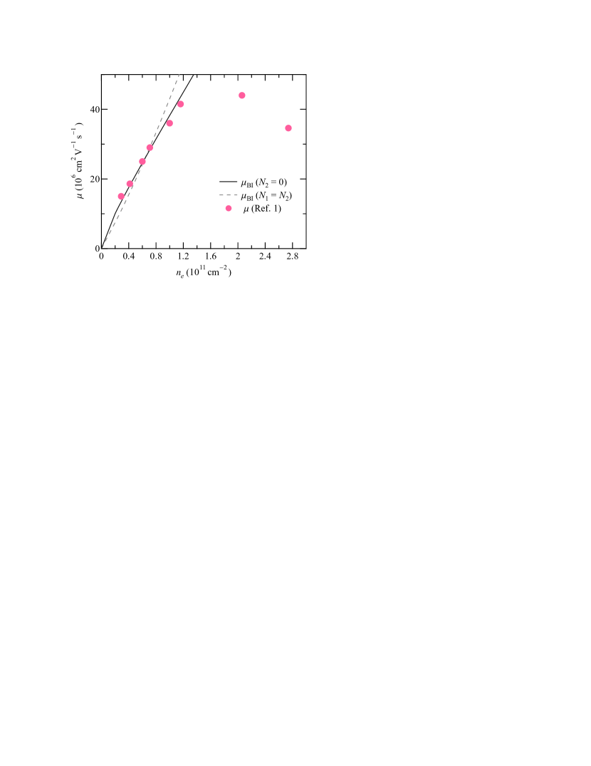
where () represents the 3D concentration of impurities in AlGaAs (GaAs). The results of our calculations for uniform impurity distribution () and for no impurities in GaAs () are shown in Fig. 1 along with the experimental data of Ref. Chung et al., 2021 (circles). We find that the data at cm-2 can be better described by cm-3 and (solid line). Assuming uniform distribution of impurities (dashed curve) yields cm-3, which is close to an estimate cm-3 of Ref. Chung et al., 2021 111This uniform impurities concentration is also close to a recent estimate found in Ref. Ahn and Das Sarma, 2022. However, they used fixed quantum well width nm in the calculations, while we take into account the density dependence such that .. We also note that is well described by , where , whereas follows , where . Here and in what follows we assume that the electron density is in units of cm-2 and the mobility is in units of cm2V-1s-1.
While BI scattering can describe the experimental data reasonably well at , it is clear that BI scattering alone cannot explain experimental at higher . Indeed, obtained power laws represent crossovers from at low Sammon et al. (2018a) to at higher Dmitriev et al. (2012). To explain the experimental at higher , one needs to examine other scattering sources.
Remote impurities. One obvious candidate for reduced at higher is remote ionized impurity scattering. For electron densities and for a given doping concentration cm-2, the fraction of ionized donors in each doping layer is small, , and we can use Eq. (22) from Ref. Sammon et al., 2018a rem ,
| (7) |
where in the final expression of Eq. (7) we used , , and wdw . Equation (7) gives at , which is more than 300 times larger than experimental , so the RI scattering is still irrelevant in this regime. We note, however, that additional mechanisms of disorder in the doping layers may lead to an increase of RI scattering, as discussed in Sec. V of Ref. Sammon et al., 2018a, although quantitative understanding of these mechanisms is still lacking.
Interface roughness. Scattering on interface roughness originates from fluctuations of the ground state energy due to monolayer local variations of the quantum well width . For the infinite barrier height (), the corresponding transport scattering rate Gold (1986, 1987) and such dependence was confirmed in narrow nm GaAs quantum wells with AlAs barriers Sakaki et al. (1987); Kamburov et al. (2016). However, in AlxGa1-xAs/GaAs quantum wells the barrier height is significantly reduced ( eV for ), and fluctuations of the ground state energy are diminished due to finite penetration of the electron wave function into the barrier Gold (1989); Li et al. (2005). As a result, is considerably suppressed compared to the case , and its dependence on weakens Gottinger et al. (1988); Li et al. (2005); Luhman et al. (2007); Kamburov et al. (2016).
We calculate the IR-limited scattering rates following the approach of Refs. Gold, 1989; Li et al., 2005. We use the barrier height for and take into account the difference in the electron effective mass in the GaAs well () and in the Al0.12Ga0.88As barriers (). At the end we also impose a constraint (wdw, ).
Using the correlator of local well width variations , where is the roughness height and is the roughness lateral size, the scattering potential due to interface roughness is given by
| (8) |
where is the ground state energy for the finite potential well. Here, the dielectric function , see Eq. (4), is computed with the form factor , see Eq. (5), using finite-potential-well wave function. (See Supplemental Material for details (not, )).
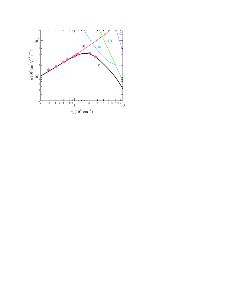
By substituting Eq. (8) into Eq. (1) we obtain the mobility due to interface roughness as shown in Fig. 2. In order to reproduce the experimental data at , we arrived at Å and Å. With these roughness parameters, becomes equal to at and, in the vicinity of this density, can be described by . We have also examined the effect of on the mobility limited by IR. By raising from 0.12 to 0.24, a value which is common for previous generation of samples, at becomes smaller by 24 %, although this effect weakens at lower .
Alloy disorder. Alloy disorder (AD) scatters electrons due to the wave function tails extending into the AlxGa1-xAs barriers. Usually, in typical high mobility samples, this scattering mechanism is deemed irrelevant, see e.g., Ref. Li et al., 2005; Umansky and Heiblum, 2013. However, in light of lower used in the new generation of samples (Chung et al., 2021), it is important to revisit this scattering source. Following Refs. Ando, 1982; Li et al., 2005; Gold, 2013, we write the scattering potential as
| (9) |
where , is the lattice constant, and eV is the conduction band discontinuity at the -point of GaAs/AlAs interface. As for the case of IR, we use finite-potential-well wave function to calculate the form factor in (see Supplementary Material (not, )). Substituting Eq. (9) into Eq. (1) and applying the constraint (wdw, ), we obtain the mobility limited by AD scattering as shown in Fig. 2. We note that can be well described by and that it becomes equal to at and to at . We thus conclude that alloy disorder scattering cannot be ignored at higher densities. We have also examined the effect of on mobility limited by alloy disorder. By increasing from 0.12 to 0.24, increases by a factor of for .
We now turn to the effects of different scattering mechanisms on quantum mobility , where the quantum scattering rate is given by
| (10) |
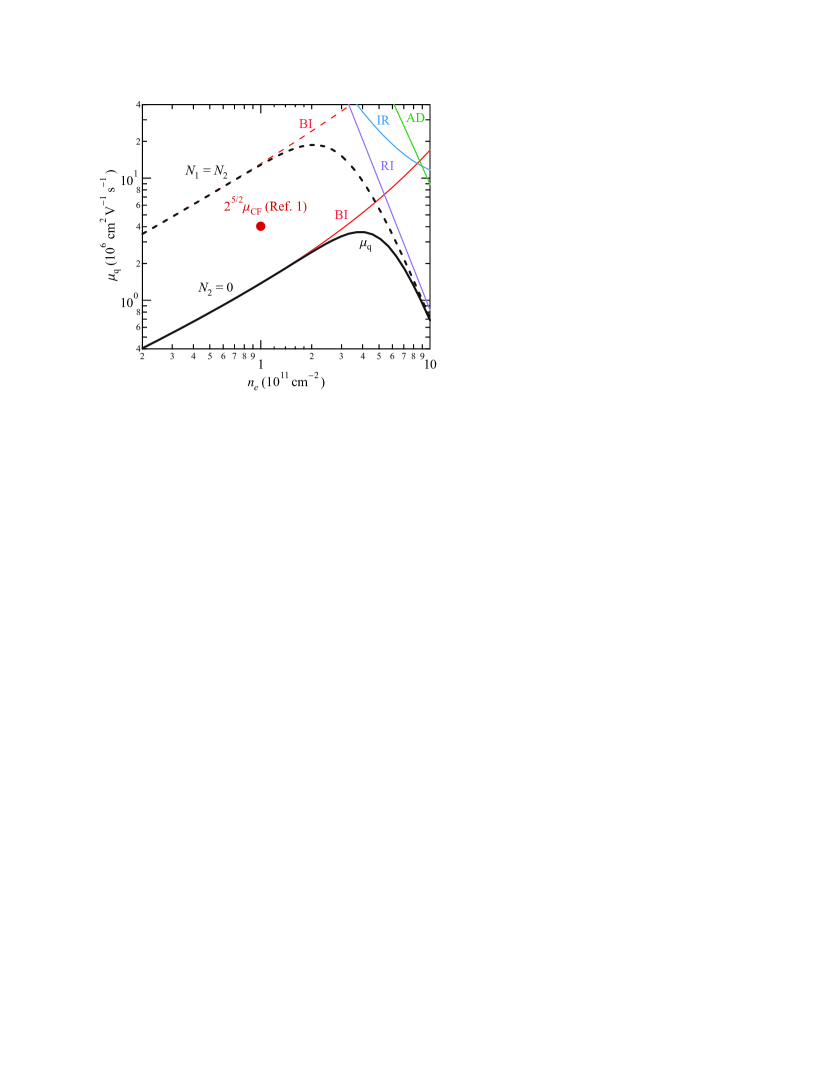
Background impurities. Since background impurities far away from the quantum well contributes to significantly, excess electron screening cannot be ignored and the scattering potential is no longer given by Eq. (3). As a very good approximation we can think of a perfect screening, such that the excess electron screening length is zero. However, the expression of scattering potential in this approximation is still cumbersome so we leave it to Supplemental Material (not, ) as a reference for an interested reader. As discussed above, two different impurity distributions, and , can describe the experimental reasonably well at . However, these distributions give very different values for , as shown in Fig. 3. Indeed, we find that (solid curve marked “BI”) is an order of magnitude smaller than (dashed curve marked “BI”). More specifically, we find that , whereas . As a result, future experiments measuring quantum mobility should be able to distinguish between these two distributions.
Remote donors. For quantum mobility limited by RI scattering, we use Eq. (23) from Ref. Sammon et al., 2018a valid at for rem :
| (11) |
where in the final expression we used , , and wdw . Even though Eq. (11) yields very large at , RI scattering is still expected to limit at higher , see Fig. 3.
Interface roughness and alloy disorder. Contributions from IR and AD can be calculated using Eqs. (8), (9), and (10). In particular we find that and . As shown in Fig. 3, these contributions are considerably smaller than the RI contribution at all relevant . As a result, one expects a crossover from BI-limited to RI-limited quantum mobility for either model of BI distribution. The value and the position of the maximum at the quantum mobility crossover should yield information on the BI distribution.
Next, we comment on the relation between the quantum mobility and the mobility of composite fermions at filling factor . By comparing the expression of the longitudinal resistivity at , Eq. (5.11) of Ref. Halperin et al., 1993,
| (12) |
and the expression for quantum mobility, Eq. (6) in Ref. Sammon et al., 2018a,
| (13) |
one can conclude that
| (14) |
which implies that . Here, is the 2D concentration of random impurities in a thin layer at a distance away from the center of the quantum well. In order to obtain and for impurities with 3D concentration , one should replace by and integrate over 222To avoid the divergence at , one can average in the denominator using , where is the wave function along direction.. This integration does not change the relation Eq. (14) between and , so that it holds for both BI and RI scattering 333On the other hand, AD and IR do not change the 2D electron concentration inside the quantum well, so they do not contribute to the gauge field fluctuations and ..
From the experimental data in Ref. Chung et al., 2021, the longitudinal resistance is at and . Using the geometry of experiments in Ref. Chung et al., 2021, we estimate . As a result, the quantum mobility at is estimated as . This data point, filled circle in Fig. 3, falls in between our predictions for and . In order to fit this point, while keeping the same as shown in Figs. 1 and 2, we need cm-3 and cm-3.
Finally, we mention that hydrodynamics (Alekseev, 2016) or scattering on oval defects (Bockhorn et al., 2014) might affect the zero-field resistivity and, as a result, the inferred mobility. Both mechanisms manifest as negative magnetoresistance in weak magnetic field (Dai et al., 2010; Hatke et al., 2011; Bockhorn et al., 2011; Hatke et al., 2012; Shi et al., 2014a, b; Bockhorn et al., 2014) which can also be seen in Fig. 3(b) of Ref. Chung et al., 2021. However, since no experimental studies of this magnetoresistance are yet available, we cannot comment on its origin.
In summary, we have examined roles of different scattering sources on the transport and quantum mobilities in the new generation of ultrahigh mobility GaAs/Al0.12As0.88 quantum wells (Chung et al., 2021). While at lower electron densities both mobilities are limited by background impurity scattering, interface roughness (remote impurity) scattering is the likely source limiting transport (quantum) mobility at large electron densities. Our predictions for quantum mobility are in agreement with the value estimated from the mobility of the composite fermions at filling factor in a sample with cm-2 Chung et al. (2021). Future measurements of quantum mobility should provide insight on the distribution of background impurities in the GaAs quantum well and in the AlGaAs barriers.
Acknowledgements.
We thank L. N. Pfeiffer and M. Shayegan for discussions and clarifying the experimental details. Y.H. was partially supported by the William I. Fine Theoretical Physics Institute. M.A.Z. acknowledges support by the U.S. Department of Energy, Office of Science, Basic Energy Sciences, under Award No. ER 46640-SC0002567.References
- Chung et al. (2021) Y. J. Chung, K. A. Villegas Rosales, K. W. Baldwin, P. T. Madathil, K. W. West, M. Shayegan, and L. N. Pfeiffer, Nature Materials 20, 632 (2021).
- (2) We note that both AD and IR scattering were not considered to be limiting factors in theories considering structures with mobilities even higher than reported in Ref. Chung et al. (2021) (see, e.g., Ref. Hwang and Das Sarma, 2008).
- Sammon et al. (2018a) M. Sammon, M. A. Zudov, and B. I. Shklovskii, Phys. Rev. Materials 2, 064604 (2018a).
- Chung et al. (2020) Y. J. Chung, K. A. Villegas Rosales, K. W. Baldwin, K. W. West, M. Shayegan, and L. N. Pfeiffer, Phys. Rev. Materials 4, 044003 (2020).
- Akiho and Muraki (2021) T. Akiho and K. Muraki, Phys. Rev. Applied 15, 024003 (2021).
- Akiho and Muraki (2022) T. Akiho and K. Muraki, arXiv:2203.14575 (2022).
- dw (2) To our knowledge, such design, which is a special case of a short-period GaAs/AlAs superlattice Baba et al. (1983); Friedland et al. (1996), was first realized in single heterointerfaces doped on one side in ’s Du et al. (1993); lor .
- (8) The condition defines maximum electron density at which the second subband of the GaAs quantum well remains unoccupied, wheres the dependence , where nm, is governed by electrostatics. These conditions were obtained from the fits to experimental data Chung et al. (2021), see Supplemental Material (not, ).
- (9) See Supplemental Material at [URL].
- (10) In our calculations we ignore the density dependence of the effective mass, which is rather weak in the considered density range (Coleridge et al., 1996; Tan et al., 2005; Hatke et al., 2013; Shchepetilnikov et al., 2017; Fu et al., 2017).
- Jonson (1976) M. Jonson, J. of Phys. C: Solid State Phys. 9, 3055 (1976).
- Gold (1986) A. Gold, Solid State Commun. 60, 531 (1986).
- Gold (1987) A. Gold, Phys. Rev. B 35, 723 (1987).
- Gold (1989) A. Gold, Zeitschrift für Physik B Condensed Matter 74, 53 (1989).
- Gold (2013) A. Gold, JETP Lett. 98, 416 (2013).
- Note (1) This uniform impurities concentration is also close to a recent estimate found in Ref. \rev@citealpahn:2022. However, they used fixed quantum well width nm in the calculations, while we take into account the density dependence such that .
- Dmitriev et al. (2012) I. A. Dmitriev, A. D. Mirlin, D. G. Polyakov, and M. A. Zudov, Rev. Mod. Phys. 84, 1709 (2012).
- (18) Eqs. (22) and (23) in Ref. Sammon et al., 2018a apply to a single doping layer. Here, we consider two doping layers playing the same role, so the mobility is reduced by 2.
- Sakaki et al. (1987) H. Sakaki, T. Noda, K. Hirakawa, M. Tanaka, and T. Matsusue, Appl. Phys. Lett. 51, 1934 (1987).
- Kamburov et al. (2016) D. Kamburov, K. W. Baldwin, K. W. West, M. Shayegan, and L. N. Pfeiffer, Appl. Phys. Lett. 109, 232105 (2016).
- Li et al. (2005) J. M. Li, J. J. Wu, X. X. Han, Y. W. Lu, X. L. Liu, Q. S. Zhu, and Z. G. Wang, Semicond. Sci. Tech. 20, 1207 (2005).
- Gottinger et al. (1988) R. Gottinger, A. Gold, G. Abstreiter, G. Weimann, and W. Schlapp, Europhys. Lett. 6, 183 (1988).
- Luhman et al. (2007) D. R. Luhman, D. C. Tsui, L. N. Pfeiffer, and K. W. West, Appl. Phys. Lett. 91, 072104 (2007).
- Umansky and Heiblum (2013) V. Umansky and M. Heiblum, Molecular Beam Epitaxy: From research to mass production, edited by M. Henini (Elsevier Inc., 2013) Chap. MBE growth of high-mobility 2DEG, pp. 121–137.
- Ando (1982) T. Ando, J. Phys. Soc. Jpn. 51, 3900 (1982).
- Halperin et al. (1993) B. I. Halperin, P. A. Lee, and N. Read, Phys. Rev. B 47, 7312 (1993).
- Note (2) To avoid the divergence at , one can average in the denominator using , where is the wave function along direction.
- Note (3) On the other hand, AD and IR do not change the 2D electron concentration inside the quantum well, so they do not contribute to the gauge field fluctuations and .
- Alekseev (2016) P. S. Alekseev, Phys. Rev. Lett. 117, 166601 (2016).
- Bockhorn et al. (2014) L. Bockhorn, I. V. Gornyi, D. Schuh, C. Reichl, W. Wegscheider, and R. J. Haug, Phys. Rev. B 90, 165434 (2014).
- Dai et al. (2010) Y. Dai, R. R. Du, L. N. Pfeiffer, and K. W. West, Phys. Rev. Lett. 105, 246802 (2010).
- Hatke et al. (2011) A. T. Hatke, M. A. Zudov, L. N. Pfeiffer, and K. W. West, Phys. Rev. B 83, 121301(R) (2011).
- Bockhorn et al. (2011) L. Bockhorn, P. Barthold, D. Schuh, W. Wegscheider, and R. J. Haug, Phys. Rev. B 83, 113301 (2011).
- Hatke et al. (2012) A. T. Hatke, M. A. Zudov, J. L. Reno, L. N. Pfeiffer, and K. W. West, Phys. Rev. B 85, 081304(R) (2012).
- Shi et al. (2014a) Q. Shi, P. D. Martin, Q. A. Ebner, M. A. Zudov, L. N. Pfeiffer, and K. W. West, Phys. Rev. B 89, 201301(R) (2014a).
- Shi et al. (2014b) Q. Shi, M. A. Zudov, L. N. Pfeiffer, and K. W. West, Phys. Rev. B 90, 201301(R) (2014b).
- Hwang and Das Sarma (2008) E. H. Hwang and S. Das Sarma, Phys. Rev. B 77, 235437 (2008).
- Baba et al. (1983) T. Baba, T. Mizutani, and M. Ogawa, Jpn. J. Appl. Phys. 22, L627 (1983).
- Friedland et al. (1996) K.-J. Friedland, R. Hey, H. Kostial, R. Klann, and K. Ploog, Phys. Rev. Lett. 77, 4616 (1996).
- Du et al. (1993) R. R. Du, H. L. Stormer, D. C. Tsui, L. N. Pfeiffer, and K. W. West, Phys. Rev. Lett. 70, 2944 (1993).
- (41) L. N Pfeiffer, private communication.
- Coleridge et al. (1996) P. Coleridge, M. Hayne, P. Zawadzki, and A. Sachrajda, Surf. Sci. 361, 560 (1996).
- Tan et al. (2005) Y.-W. Tan, J. Zhu, H. L. Stormer, L. N. Pfeiffer, K. W. Baldwin, and K. W. West, Phys. Rev. Lett. 94, 016405 (2005).
- Hatke et al. (2013) A. T. Hatke, M. A. Zudov, J. D. Watson, M. J. Manfra, L. N. Pfeiffer, and K. W. West, Phys. Rev. B 87, 161307(R) (2013).
- Shchepetilnikov et al. (2017) A. V. Shchepetilnikov, D. D. Frolov, Y. A. Nefyodov, I. V. Kukushkin, and S. Schmult, Phys. Rev. B 95, 161305(R) (2017).
- Fu et al. (2017) X. Fu, Q. A. Ebner, Q. Shi, M. A. Zudov, Q. Qian, J. D. Watson, and M. J. Manfra, Phys. Rev. B 95, 235415 (2017).
- Ahn and Das Sarma (2022) S. Ahn and S. Das Sarma, Phys. Rev. Materials 6, 014603 (2022).
- Sammon et al. (2018b) M. Sammon, T. Chen, and B. I. Shklovskii, Phys. Rev. Materials 2, 104001 (2018b).
- Davies (1997) J. H. Davies, The Physics of Low-dimensional Semiconductors: An Introduction (Cambridge University Press, 1997).
- Note (4) Since background impurities scattering dominates at , and we can use from Ref. \rev@citealpsammon:2018a.
- Note (5) See for example, Eq. (5c) in Ref. \rev@citealpgold:1989b or Section 4.9 in Ref. \rev@citealpdavies:1997.
I Supplementary materials
I.1 Well width and setback versus electron density
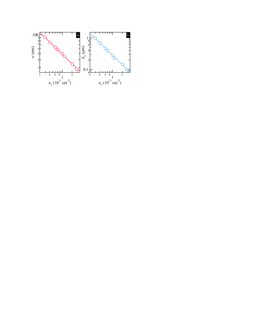
To obtain the constraints on the quantum well width and on the effective spacer width we have fitted the experimental data of Ref. Chung et al., 2021 as illustrated in Fig. S1. Open circles in panel (a) and (b) of Fig. S1 represent and , respectively, as a function of electron density . Solid lines are power law fits to the data, yielding and , in units as marked. These relationships are equivalent to , where is the Fermi wave number, and , where nm, used in the main text. Here, the first condition corresponds to a maximum electron density at which the second subband of the GaAs quantum well still remains unoccupied, whereas the second condition is governed by electrostatics of the device.
I.2 Scattering potential of a single background impurity
We derive the screened potential of a single charged impurity at a distance away from the center of a quantum well of thickness using random phase approximation (RPA) as in Ref. Sammon et al., 2018a. There are two sources of screening for background impurities: they can be screened by 2DEG in the quantum well or by excess electrons (EEs) remaining in the remote doping wells separated from the center of the 2DEG by distance . We introduce the notations for the screened impurity interaction and for the unscreened impurity interaction, where the subscript i denotes the impurity and subscript can be equal to 1 (2DEG) or 2 (EEs). [Used below subscript can be equal to 1 (2DEG) or 2 (EEs) as well]. Following Ref. Sammon et al., 2018a, we obtain the screened Coulomb interaction between an impurity and an electron in the 2DEG,
| (S1) |
where bare interactions and are given by
| (S2) | |||
| (S3) |
Here, and are the linear densities of the 2DEG and of the EEs respectively, and the polarization functions and are calculated using Thomas-Fermi approximation with local field corrections.
Within infinite-potential-well approximation, , we can write down the analytical expressions for bare interactions. For , we find
| (S4) |
where
| (S5) |
and
| (S6) |
For , we have
| (S7) |
The electron-electron interactions are given by
| (S8) |
| (S9) |
| (S10) |
where
| (S11) |
Screening by EEs affects only the potential of impurities located in the vicinity of the doping wells. These impurities practically do not contribute to momentum relaxation, so we can calculate the mobility assuming . The corresponding in Eq. (S1) with can be simplified as
| (S12) |
which is equal to defined in Eq. (3) of the main text. However, for quantum mobility EE screening plays an important role. The screening radius of EEs is given by Sammon et al. (2018b), valid for large filling fraction of remote donors 444 Since background impurities scattering dominates at , and we can use from Ref. Sammon et al., 2018b. , where is the 2DEG density and cm-2 is the concentration of donors. We have confirmed that our results for with nm are practically the same as for or .
I.3 Finite-potential-well solution
The Schrödinger equation is given by
| (S13) |
where at and at , and the effective finite potential well is described by
| (S14) |
where meV () and is the Fermi energy. Below we use to represent for simplicity. The bound state solutions () for the lowest subband are
| (S15) |
where , . At , is continuous while has a finite discontinuity because of the difference in effective masses:
| (S16) | |||
| (S17) |
The normalization of gives
| (S18) |
Combining with Eq. (S16), one has
| (S19) |
By dividing Eq. (S17) by Eq. (S16), one obtains
| (S20) |
Introducing dimensionless quantities , , where is the ground state energy for infinite well, in Eq. (S20) we arrive at 555See for example, Eq. (5c) in Ref. Gold, 1989 or Section 4.9 in Ref. Davies, 1997.
| (S21) |
If and , then . For any finite , we have . For example, at small electron concentration cm-2 with , we have , which justifies our infinite-potential-well approximation at lower . On the other hand, at large electron concentration cm-2, decreased significantly from 6.2 to 1.1, and therefore finite-potential-well effect such that has to be taken into account.
The local energy fluctuation due to interface roughness is given by
| (S22) |
where is the local variation of the well width at a position . Taking derivative with respect to for both sides in Eq. (S21), we obtain the expression for
| (S23) |
and
| (S24) |
Substituting Eq. (S23) in Eq. (8) in the main text, we obtain the scattering potential for the interface roughness.