Electronic-photonic circuit crossings
††preprint: APS/123-QEDElectrical control of light in integrated photonics is central to a wide range of research and applications. It is conventionally achieved with thermo-optic tuning, but this suffers from high energy consumption and crosstalk. These challenges could be resolved with nanoelectromechanical photonics but scalable platforms were so far not demonstrated because of incompatibility with conventional multilayer metal architectures and because conventional approaches do not allow crossings of electrical wires and photonic waveguides. Here we use topology optimization to devise a single-layer electronic-photonic circuit crossing with up to optical transmission across an isolation trench with excellent electrical isolation. We use the crossing to demonstrate a monolithic silicon nano-electro-mechanical add-drop switch in which the flow of photons, electrons, and mechanical motions are fully integrated within the same layer. Our work enables hitherto impossible opto-electro-mechanical topologies and may lead to new functionalities in nano-opto-electro-mechanical systems, optomechanics, and integrated quantum photonics.
Information technologies rely on controlling two fundamentally different particles: electrons are strongly interacting massive charged fermions while photons are massless and charge-neutral bosons that do not interact. These differences underpin the development of optical communication systems based on low losses and high coherence as well as electronic computing relying on strong interactions. For many reasons, however, integrating electronics and photonics is becoming an increasingly important research frontier: First, a sizeable fraction of the energy consumption in modern computing is spent on routing information through lossy electrical leads, which may be significantly reduced by chip-level optical interconnects [1, 2]. Second, the developments in hybrid quantum technologies call for high-fidelity interfaces between stationary and flying qubits [3, 4], which require unprecedented control and integration of electronics and photonics. Third, the integration of photonics and electronics is at the heart of a wide range of new technologies that rely on advanced nanofabrication for new applications beyond electronics [5], ranging from smart sensors [6] over ultrahigh-bandwidth optical networks [7] to chip-scale particle accelerators [8], and nano-opto-electro-mechanical systems (NOEMS) [9, 10].
Simultaneously controlling the flow of electrons and photons inside the same microchip is challenging because of the conflicting requirements for electronics and photonics: Electronic wires rely on conduction by free electrons but they in turn lead to significant optical losses. Therefore, both research and technology has so far resorted to various multi-layer chip architectures aiming to avoid crossings between wires and waveguides. Existing solutions include optical layers embedded in transparent insulators with metallic surface electrode layers or numerous patterned conducting layers buried below the optical layers and contacted by deep vias in order to route the electrical signals without impeding the optical performance. Common to existing solutions is the need to add more layers or processes as the circuits grow. In other words, the circuit complexity scales superlinearly with the number of (avoided) electronic-photonic crossings. While these solutions can be employed to integrate photonic circuits with CMOS chips [11, 12, 13], they are now a limitation for a wide range of research including routing of single photons from quantum dots [14], chip-scale LiDAR solutions [15, 6], photonic interconnects for 5G networks [16], compact sensors [17], electro-optic and thermo-optic devices [18, 19], and nano-electro-mechanical photonic switches [20]. The solution proposed in this work overcomes the system-level complexity in routing electrons and photons inside the chip by introducing a carefully engineered and inversely designed monolithic device. It allows crossing electronic connections and photonic waveguides using the same device layer without introducing significant electrical resistance or optical losses. We focus our effort on silicon membranes fabricated on the silicon on insulator (SOI) platform but the concepts can be readily applied to all other semiconductor platforms.
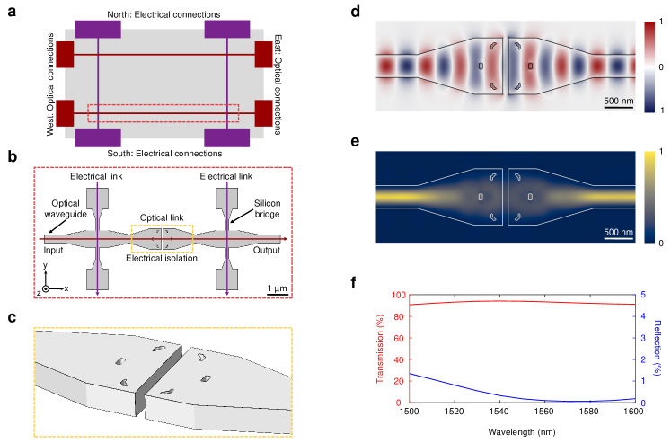
Figure 1a illustrates a generic circuit topology for routing electrons and photons where photons are guided through the optical links, i.e., photonic waveguides. The optical ports are oriented east-west (EW) while the electrical contacts are oriented north-south (NS). Except for the most primitive integrated electronic-photonic ciruits, it is impossible to build such architectures without introducing either multilayer technologies or resorting to circuit topologies that involve crossings of photonic waveguides and electronic wires. The immediately apparent challenge of designing an electronic-photonic circuit crossing (EPCC) is to achieve both high optical transmission and low reflection in the EW direction as well as low electrical resistance in the NS direction. Furthermore, an important additional requirement for generic multiport devices is that the electrical resistance must be very high in the EW direction to avoid short circuits between the electrical leads. A simple solution would be to introduce an isolation trench through the waveguide to provide electrical isolation but this is clearly a sub-optimal solution as it significantly reduces the optical transmission. For example, introducing a gap of in a suspended waveguide results in a transmission of less than and a reflection above over a bandwidth centered at (fig. S1). Alternative approaches relying on parameter-optimized tapering (fig. S2) is also resulting in so poor performance that is detrimental to devices with even a minimum of system-level complexity.
An EPCC solution must ensure proper mode matching across the isolation trench. Due to the coherent nature of the photon scattering and interference, designing such a subwavelength mode-matching EPCC is a complicated and non-intuitive problem. We therefore employ inverse design by topology optimization [21, 22] to develop a compact and scalable device that transmits photons efficiently across the electrical isolation trench. The trench must be wide enough to avoid electric breakdown due to Townsend avalanches and field emission. For our experiments, we consider trenches that provide electrical isolation for a voltage of at least [23], suitable for high-voltage applications including NOEMS. As we are interested in maximizing the transmission across a isolation trench, while at the same time minimizing reflections, we seek to maximize the figure of merit, , where denotes transmission across the isolation trench and the reflection, over a spatial region of that corresponds to the length and width of the design domain. The parameter is added to the denominator to avoid numerical issues as caused by the singularity at as well as to balance the priority to vs such that the optimization algorithm will not sacrifice when . The EPCC is optimized at the wavelengths corresponding to the beginning and the end of the targeted bandwidth, i.e., and , in order to ensure the efficient performance across a bandwidth centered at .
Figure 1b illustrates our solution to the EPCC problem. The photonic waveguide is suspended by silicon bridges designed to provide mechanical support without disturbing the propagating optical mode, while at the same time serving as electrical links in the NS-direction. The central part is shown in Fig. 1c and is generated by topology optimization, which results in excellent transmission. This is evident from the lack of resonances in the electric field (Fig. 1d) and time-averaged power flow (Fig. 1e) of the transverse-electric mode. The calculated transmission and reflection spectra are shown in Fig. 1f and feature a transmission of and a reflection of over a bandwidth as well as a peak transmission of , which is a dramatic improvement compared to the solutions before topology optimization (figs. S1 and S2).
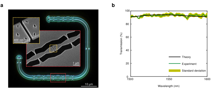
In order to experimentally verify these findings, we fabricate a set of photonic circuits with 0 to 6 EPCCs in series using electron-beam lithography and cryogenic deep reactive ion etching applied to SOI wafers. This enables direct measurement of the insertion loss of a single EPCC using the cut-back method, which separates the coupling losses from propagation losses. Figure 2a shows a dark-field microscope image of such a circuit comprised of 6 EPCCs embedded in a single-mode waveguide, 20 silicon bridges, and two cross-polarized input/output couplers. The position and number of silicon bridges are chosen to provide mechanical stability for maintaining the photonic circuit suspended. Six different sets of each photonic circuit are fabricated on the same chip, which allows us to do ensemble measurements and carefully estimate the standard deviation. Figure 2b compares the experimental transmission spectrum with the numerical calculations and shows excellent agreement.
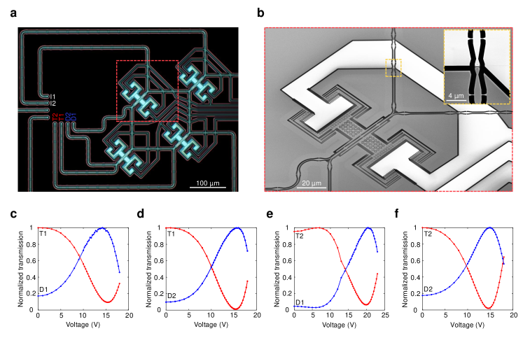
To illustrate the application of the EPCC, we consider a new type of monolithic electro-mechanical photonic add-drop network that integrates EPCCs with nano-electro-mechanical photonic switches in a single lithographic step. Figure 3a shows a dark-field microscope image of the switch network. The network is built on four reconfigurable directional couplers controlled by electrostatic comb-drive actuators (Fig. 3b), which can induce nanoscale displacements [24] to the mechanically compliant waveguides and thereby change the configuration of the switching network. The light coupled to the input () can be transmitted to the corresponding through port () or directed to any of the drop ports and depending on the driving voltage of the activated comb-drive actuator. Figure 3b shows a scanning electron micrograph of one of the switching elements and illustrates how isolation trenches along with the EPCCs are introduced to the device layer of the SOI wafer to route the electrical signals to the comb-drive actuator. The through- and drop-port transmission at is plotted in Fig. 3c-f and show a clear switching behavior for all voltages. This demonstrates central building blocks for programmable [25, 26] or quantum photonic circuits [18] where the full benefit of the EPCC is ultimately harvested in larger networks: Regardless of topology and complexity, advanced electronic-photonic circuits can be fabricated in the same device layer and in a single lithography step.
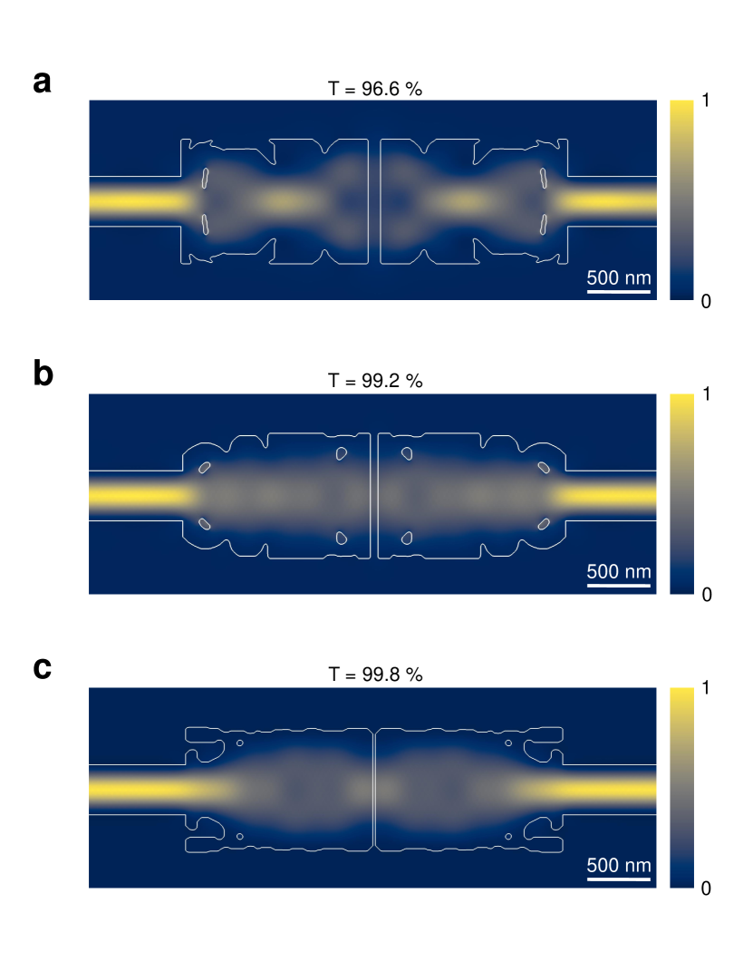
For larger networks, the optical transmission becomes a limiting factor and we therefore design additional EPCCs while relaxing the bandwidth requirement and allowing for smaller but still feasible gaps [27]. Figure 4 shows EPCCs for (a) , (b) , and (c) isolation gaps topology-optimized for maximum transmission at . The transmission increases with decreasing gap size and for a gap of , the peak power transmission reaches a remarkably high value of . Furthermore, it remains above across a bandwidth (fig. S6). Because the overall transmission of circuits with crossings scales as , a power transmission of implies that hundreds of EPCCs in series would result in insertion losses below . This shows that highly complex hybrids of nanoelectronics, nanophotonics, and nanomechanics can be integrated with negligible losses. Our results indicate that even higher transmission is attainable for smaller gaps.
The EPCC opens perspectives for a wide range of new research and technology. For example, isolation trenches are not only efficient electrical isolators, they are also ideal for thermal isolation in nanophotonic devices [19] or mechanical isolation for quantum optomechanics [28], and we envision our technology enabling, e.g., phonon-photon crossings. In addition, our concepts apply directly to other semiconductor platforms such as gallium arsenide or indium phosphide, where they enable independent electrical control of quantum emitters in integrated photonic circuits [14], thus solving a major scaling problem in integrated quantum photonics and enabling unprecedented circuit topologies in integrated photonics. Our experiment probes parameters ideal for low transmission losses and high operating voltages to actuate stiff springs in quasistatic nano-electro-mechanical switching scenarios but EPCCs can be applied immediately to other regimes. For example, local doping of the suspension bridges could reduce resistances, and thus, -times, by orders of magnitude without introducing significant optical losses, which would bring the EPCCs into the realm of CMOS-compatible low-voltage high-speed applications.
References
- Miller [2009] D. A. Miller, Device requirements for optical interconnects to silicon chips, Proc. IEEE 97, 1166 (2009).
- Ayata et al. [2017] M. Ayata, Y. Fedoryshyn, W. Heni, B. Baeuerle, A. Josten, M. Zahner, U. Koch, Y. Salamin, C. Hoessbacher, C. Haffner, D. L. Elder, L. R. Dalton, and J. Leuthold, High-speed plasmonic modulator in a single metal layer, Science 358, 630 (2017).
- Elshaari et al. [2020] A. W. Elshaari, W. Pernice, K. Srinivasan, O. Benson, and V. Zwiller, Hybrid integrated quantum photonic circuits, Nat. Photonics 14, 285 (2020).
- Lodahl et al. [2015] P. Lodahl, S. Mahmoodian, and S. Stobbe, Interfacing single photons and single quantum dots with photonic nanostructures, Rev. Mod. Phys. 87, 347 (2015).
- Waldrop [2016] M. M. Waldrop, The chips are down for Moore’s law, Nature 530, 144 (2016).
- Rogers et al. [2021] C. Rogers, A. Y. Piggott, D. J. Thomson, R. F. Wiser, I. E. Opris, S. A. Fortune, A. J. Compston, A. Gondarenko, F. Meng, X. Chen, G. T. Reed, and R. Nicolaescu, A universal 3D imaging sensor on a silicon photonics platform, Nature 590, 256 (2021).
- Levy et al. [2010] J. S. Levy, A. Gondarenko, M. A. Foster, A. C. Turner-Foster, A. L. Gaeta, and M. Lipson, CMOS-compatible multiple-wavelength oscillator for on-chip optical interconnects, Nat. Photonics 4, 37 (2010).
- Sapra et al. [2020] N. V. Sapra, K. Y. Yang, D. Vercruysse, K. J. Leedle, D. S. Black, R. J. England, L. Su, R. Trivedi, Y. Miao, O. Solgaard, R. L. Byer, and J. Vučković, On-chip integrated laser-driven particle accelerator, Science 367, 79 (2020).
- Midolo et al. [2018] L. Midolo, A. Schliesser, and A. Fiore, Nano-opto-electro-mechanical systems, Nat. Nanotechnol. 13, 11 (2018).
- Haffner et al. [2019] C. Haffner, A. Joerg, M. Doderer, F. Mayor, D. Chelladurai, Y. Fedoryshyn, C. I. Roman, M. Mazur, M. Burla, H. J. Lezec, V. A. Aksyuk, and J. Leuthold, Nano–opto-electro-mechanical switches operated at CMOS-level voltages, Science 366, 860 (2019).
- Miller [2000] D. Miller, Rationale and challenges for optical interconnects to electronic chips, Proc. IEEE. 88, 728 (2000).
- Atabaki et al. [2018] A. H. Atabaki, S. Moazeni, F. Pavanello, H. Gevorgyan, J. Notaros, L. Alloatti, M. T. Wade, C. Sun, S. A. Kruger, H. Meng, and K. Al Qubaisi, Integrating photonics with silicon nanoelectronics for the next generation of systems on a chip, Nature 556, 349 (2018).
- Stojanović et al. [2018] V. Stojanović, R. J. Ram, M. Popović, S. Lin, S. Moazeni, M. Wade, C. Sun, L. Alloatti, A. Atabaki, F. Pavanello, N. Mehta, and P. Bhargava, Monolithic silicon-photonic platforms in state-of-the-art CMOS SOI processes [Invited], Opt. Express 26, 13106 (2018).
- Papon et al. [2019] C. Papon, X. Zhou, H. Thyrrestrup, Z. Liu, S. Stobbe, R. Schott, A. D. Wieck, A. Ludwig, P. Lodahl, and L. Midolo, Nanomechanical single-photon routing, Optica 6, 524 (2019).
- Trocha et al. [2018] P. Trocha, M. Karpov, D. Ganin, M. H. P. Pfeiffer, A. Kordts, S. Wolf, J. Krockenberger, P. Marin-Palomo, C. Weimann, S. Randel, W. Freude, T. J. Kippenberg, and C. Koos, Ultrafast optical ranging using microresonator soliton frequency combs, Science 359, 887 (2018).
- Sabella [2020] R. Sabella, Silicon photonics for 5G and future networks, IEEE J. Sel. Top. Quantum Electron. 26, 8301611 (2020).
- Yang et al. [2021] Z. Yang, T. Albrow-Owen, W. Cai, and T. Hasan, Miniaturization of optical spectrometers, Science 371, 6528 (2021).
- Arrazola et al. [2021] J. M. Arrazola et al., Quantum circuits with many photons on a programmable nanophotonic chip, Nature 591, 54 (2021).
- Souza et al. [2018] M. C. Souza, A. Grieco, N. C. Frateschi, and Y. Fainman, Fourier transform spectrometer on silicon with thermo-optic non-linearity and dispersion correction, Nat. Commun. 9, 665 (2018).
- Seok et al. [2016] T. J. Seok, N. Quack, S. Han, R. S. Muller, and M. C. Wu, Large-scale broadband digital silicon photonic switches with vertical adiabatic couplers, Optica 3, 64 (2016).
- Bendsøe and Sigmund [2013] M. P. Bendsøe and O. Sigmund, Topology optimization: Theory, methods, and applications (Springer Science & Business Media, 2013).
- Christiansen and Sigmund [2021] R. E. Christiansen and O. Sigmund, Inverse design in photonics by topology optimization: tutorial, J. Opt. Soc. Am. B 38, 496 (2021).
- Peschot et al. [2014] A. Peschot, N. Bonifaci, O. Lesaint, C. Valadares, and C. Poulain, Deviations from the paschen’s law at short gap distances from 100 nm to 10 µm in air and nitrogen, Appl. Phys. Lett. 105, 123109 (2014).
- Tsoukalas et al. [2020] K. Tsoukalas, B. Vosoughi Lahijani, and S. Stobbe, Impact of transduction scaling laws on nanoelectromechanical systems, Phys. Rev. Lett. 124, 223902 (2020).
- Bogaerts et al. [2020] W. Bogaerts, D. Pérez, J. Capmany, D. A. B. Miller, J. Poon, D. Englund, F. Morichetti, and A. Melloni, Programmable photonic circuits, Nature 586, 207 (2020).
- Carolan et al. [2015] J. Carolan, C. Harrold, C. Sparrow, E. Martin-López, N. J. Russell, J. W. Silverstone, P. J. Shadbolt, N. Matsuda, M. Oguma, M. Itoh, G. D. Marshall, M. G. Thompson, J. C. F. Matthews, T. Hashimoto, J. L. O’Brien, and A. Laing, Universal linear optics, Science 349, 711 (2015).
- Albrechtsen et al. [2021] M. Albrechtsen, B. Vosoughi Lahijani, R. E. Christiansen, V. T. H. Nguyen, L. N. Casses, S. E. Hansen, N. Stenger, O. Sigmund, H. Jansen, J. Mørk, and S. Stobbe, Nanometer-scale photon confinement inside dielectrics, arXiv:2108.01681 (2021).
- Rossi et al. [2018] M. Rossi, D. Mason, J. Chen, Y. Tsaturyan, and A. Schliesser, Measurement-based quantum control of mechanical motion, Nature 563, 53 (2018).
ACKNOWLEDGMENTS
Funding: We gratefully acknowledge financial support from the Villum Foundation Young Investigator Program (Grant No. 13170), the Danish National Research Foundation (Grant No. DNRF147 - NanoPhoton), Innovation Fund Denmark (Grant No. 0175-00022 - NEXUS), and Independent Research Fund Denmark (Grant No. 0135-00315 - VAFL). Author contributions: B.V.L., M.A., and S.S. conceived the concepts. S.S. supervised the project. R.E.C., B.V.L., and C.A.R. designed the electronic-photonic circuit crossings and performed the numerical calculations. B.V.L., M.A., M.T.S., and S.S. designed the chips. M.A. and C.A.R. fabricated the samples. B.V.L. and M.A. carried out the experiments. B.V.L., M.A., C.A.R., K.T., and S.S. contributed to theory and data analysis. B.V.L. and S.S. wrote the manuscript with contributions and input from all authors. Competing interests: Part of the work is subject to a patent application by M.A., B.V.L., S.S., and R.E.C. The remaining authors declare no competing interests. Data and materials availability: All data are available in the manuscript or the supplementary materials.