Tip-induced excitonic luminescence nanoscopy of an atomically-resolved van der Waals heterostructure
Abstract
Low-temperature scanning tunneling microscopy is used to probe, with atomic-scale spatial resolution, the intrinsic luminescence of a van der Waals heterostructure, made of a transition metal dichalcogenide monolayer stacked onto a few-layer graphene flake supported by an Au(111) substrate. Sharp emission lines arising from neutral, charged and localised excitons are reported. Their intensities and emission energies vary as a function of the nanoscale environment of the van der Waals heterostructure, explaining the variability of the emission properties observed with diffraction-limited approaches. Our work paves the way towards understanding and control of optoelectronic phenomena in moiré superlattices with atomic-scale resolution.
Introduction
Van der Waals (vdW) heterostructures made from stacks of two-dimensional (2D) materials, in particular semiconducting transition metal dichalcogenides (TMDs), are ideal systems for studying fundamental phenomena related to the confinement of tightly bound excitons Wang et al. (2018) and their exploitation in atomically thin optoelectronic devices Mak and Shan (2016); Wilson et al. (2021). The rich physics of excitons, trions (i.e., charged excitons) and more complex many-body states in TMDs and related vdW heterostructures has been addressed through optical spectroscopy Wang et al. (2018); Shree et al. (2021), in particular by recording their micro-photoluminescence (PL) characteristics, with a diffraction-limited spatial resolution of typically . These far-field optical studies have highlighted significant spatial variations in the optical response of a given sample, due to inhomogeneities of the nanoscale environment, including strain gradients Harats et al. (2020), dielectric disorder Raja et al. (2019), as well as to localised defects Tongay et al. (2013a); Chow et al. (2015) and dopants Tongay et al. (2013b). Taking advantage of these subtle structure/property relationships, periodic nanoscale moiré super-potentials resulting from the controlled rotational mismatch between stacked 2D layers have recently been used to tailor exciton physics, with potential outcomes for quantum simulation and quantum technologies Tang et al. (2020); Li et al. (2021); Wilson et al. (2021); Kennes et al. (2021). Understanding of such emergent phenomena requires addressing excitons and their local-environment with a spatial resolution below the moiré wavelength () and the exciton Bohr radius ()Yu et al. (2017); Huang et al. (2022), i.e., two to three orders of magnitude below the optical diffraction limit.
Recently, attempts have been made to address excitons in TMDs with nanoscale resolution Park et al. (2018); Darlington et al. (2020); Bonnet et al. (2021); Pommier et al. (2019); Péchou et al. (2020); Peña Román et al. (2020); Zhang et al. (2022). In particular, tip-enhanced PL studies have provided original ways to control the emission characteristics of TMD monolayers Park et al. (2018) as well as to image nanoscale strain gradients Darlington et al. (2020) in ambient conditions with a resolution of 15 nm. In parallel, atomically-resolved luminescence has been reported on single molecules using scanning tunneling microscopy-induced luminescence (STML)Qiu et al. (2003); Wu et al. (2008); Zhang et al. (2016); Doppagne et al. (2017); Zhang et al. (2017a); Doppagne et al. (2018); Kimura et al. (2019), a method that was recently applied to investigate excitonic emission from TMDs in ambient air Pommier et al. (2019); Péchou et al. (2020); Peña Román et al. (2020). Under these conditions, atomic-scale resolution could not be attained, probably because of atmospheric contamination and lack of mechanical and thermal stability. Attempts to address the excitonic properties of TMDs with STM in ultra-high vacuum (UHV) at cryogenic temperatures have been reported Krane et al. (2016); Schuler et al. (2020), but the luminescence signals were dominated by inelastic transitions between electrodes and TMD states, whereas radiative recombination of excitons and trions was likely quenched by the strong interaction with the supporting metallic substrate Velický et al. (2018). Approaches allowing investigating excitonic emission from vdW heterostructures at the atomic scale are highly desirable, but still lacking.
In this article, we take up this challenge and demonstrate intrinsic excitonic luminescence from a two-dimensional semiconductor with the nanoscale-resolution provided by low-temperature STML. We show that a vdW heterostructrure based on a TMD monolayer, decoupled from an Au(111) crystal by a few-layer graphene flake (FLG) allows preserving its luminescence while ensuring optimal STM imaging of surface atoms and moiré superlattices. Our results provide insights into the mechanisms leading to STM-induced luminescence in vdW heterostructures and further establish STM-based methods as a unique tool to correlate the optical response of low-dimensional systems to their nano- and atomic-scale environment.
Results and discussion
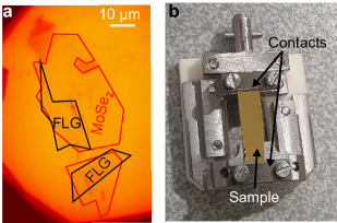
Our measurements were performed on a vdW heterostructure made of a molybdenum diselenide (MoSe2 ) monolayer stacked on top of a few layer () graphene flake (FLG) deposited onto an Au(111) substrate (see Methods and Supplementary Section S1 for more details). Figure 1a, b and c show a schematic representation of the STM-induced luminescence (STML) experiment, as well as an optical image of the MoSe2/FLG/Au(111) heterostructure and an atomically-resolved constant current STM image, respectively. As further discussed below, a STM silver (Ag) tip is used to locally generate excitonic electroluminescence from the MoSe2 monolayer. Here, akin to hexagonal boron nitride (hBN) Dean et al. (2010); Cadiz et al. (2017), the FLG provides a smooth substrate for the TMD, while ensuring efficient electrical conduction. This configuration also makes use of the plasmonic properties of the Ag-tip Au-substrate junction (Fig. 1a), which is known to enhance radiative recombination in STML experiments Rosławska et al. (2022), leading to an optimal configuration to detect excitonic luminescence.
We first report on low temperature PL measurements recorded ex situ using a laser beam of in diameter at various close-lying spots on the sample, indicated in Fig. 1b. The strikingly different PL spectra shown in Fig. 1d suggest sizeable inhomogeneities at the sub-micrometre scale. These inhomogeneities are likely due to the necessary thermal annealing step performed before introducing the sample into the STM chamber (see Methods) and are further resolved using STML, as discussed in Fig. 2 and 3.
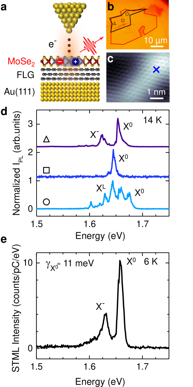
Three types of low temperature PL spectra are identified on the MoSe2/FLG/Au(111) region shown in Fig. 1b (see Supplementary Section 2 for a detailed analysis). First, we observe spectra dominated by a high-energy emission line near 1.65 eV, followed by a lower intensity feature, situated about 30 meV below the main line (top trace in Fig. 1d). Based on well-established literature Ross et al. (2013); Wang et al. (2015), the main and lower energy lines are safely assigned to the bright neutral exciton () and to the negative trion (), respectively. The negatively charged nature of the trion will be discussed in details below. Next, we also observe spectra that only display emission from the line (middle trace in Fig. 1d), as well as considerably more complex spectra, showing a variety of sharper, spatially dependent and spectrally diffusing features assigned to localised excitons Branny et al. (2016) (bottom trace in Fig. 1d). These distinct behaviours are directly related to the quality of the MoSe2/FLG and FLG/Au interfaces. In the event of a tight coupling between flat MoS2 and FLG, we expect an efficient “filtering effect” to take place Lorchat et al. (2020), which yields single line spectra akin to the middle trace in Fig. 1d. This effect stems from complete neutralisation of the MoSe2 layer by FLG, together with efficient PL quenching of long-lived localised excitons through non-radiative energy transfer to the FLG, a decay pathway that affects the short-lived emission to a much lesser extent Lorchat et al. (2020). Hence, the observation of and emission (top trace in Fig. 1d) suggests partial decoupling between the top MoSe2 layer and the FLG/Au(111) underneath. Dominant emission from localised states (bottom trace in Fig. 1d) may stem from the local conformation of the MoSe2 layer to the underlying substrate made rougher by thermal annealing. These observations are consistent with complementary PL measurements on MoSe2 monolayers directly deposited onto a thermally evaporated polycristalline Au film Lorchat et al. (2020).
In such an heterogeneous landscape, STM allows one to probe the topography of a localised area with a resolution down to the atomic scale, making it possible to select regions that are uniform over hundreds of nm2, or individual defects, and eventually address their STML properties. In Fig. 1e, we show a typical STML spectrum recorded with the STM tip localised on top of an atomically-resolved area of the MoSe2/FLG/Au(111) heterostructure shown in Fig. 1c. This spectrum is characterised by a prominent emission line located at 1.659 0.001 eV with a lower-intensity feature at 1.630 0.001 eV. These two emission lines have full-width at half maximum (FWHM) of 11 meV and 14 meV, respectively. Comparison with the PL spectra discussed above allows us to assign the high and low-energy emission lines to and , respectively. These spectra provide by far the sharpest excitonic emission lines achieved in STML measurements on TMDs and are the first example where intrinsic luminescence is obtained with the stability and cleanness required for atomically-resolved imaging of the TMD atomic registry. We conclude that the presence of the FLG interlayer preserves the low-temperature luminescence yield of the supported MoSe2 that would otherwise be massively quenched by non-radiative decay channels to the underlying Au(111) substrate Krane et al. (2016); Peña Román et al. (2020); Velický et al. (2018).
The FWHM fitted from our STML spectra, even for the sharpest example (2.9 meV, see Fig. 2e), still exceeds the homogeneous limit expected in monolayer MoSe2-based vdW heterostructures (eV FWHM for a typical lifetime of 2 ps) Fang et al. (2019). This extra broadening may find its origin in the electronic coupling between TMD and FLG as well as in the excitonic lifetime reduction due to the Purcell effect taking place at the plasmonic tip-sample cavity Rosławska et al. (2022).
We estimate an overall quantum yield of photons/e- (assuming an overall detection efficiency of 10) a value that is orders of magnitude lower than the one reported for single molecules in STML experiments Wu et al. (2008). This rather small emission yield suggests that non-radiative exciton decay plays a significant role here. This behaviour may be assigned to the metallic character of graphene that has been shown to efficiently quench hot excitons prior to their relaxation down to the light cone Lorchat et al. (2020); Robert et al. (2016). Alternatively, the low electroluminescence yield may reflect an intrinsically weak exciton formation probability, a mechanism that is further discussed below.
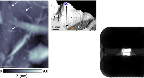
STML can be used to identify and characterize inhomogeneities occurring at the scale of atoms up to a few hundreds of nanometres, and how they affect luminescence properties. To this end, we first recorded a STM image (Fig. 2a) on a typical area of the heterostructure that approximately corresponds to the area covered by a diffraction-limited laser spot. This image displays flat and well-organised areas separated by ripples, folds and protrusions (arrows in Fig. 2(a)) that stem from the conformation of the heterostructure to the underlying Au(111) substrate. These protrusions, typically 1 nm-high – 10 nm-wide, often referred to as nano-bubblesDarlington et al. (2020), correspond to areas where the TMD and the FLG are slightly decoupled, most likely because of remaining organic adsorbates at the interfaces between MoSe2, FLG and Au(111). These adsorbates segregate locally thanks to the so-called self-cleaning mechanism inherent to 2D materials Castellanos-Gomez et al. (2014). This mechanism that separates clean and flat regions from nano- or microscale pockets of residues is favoured by the annealing step. A pseudo-3D image of one of these protrusions located next to a flat area is provided in Fig. 2b.
STML spectra acquired on top of the protrusion, and 5 nm away on the nearby flat region are displayed in Fig. 2c. On the flat area, the spectrum (in orange) is characterised by an line at 1.590 0.001 eV and by the absence of trion emission, as we shall discuss below. On top of the nano-bubble,the emission (in blue) is much brighter (by a factor of ) indicating a reduced quenching by the underlying FLG. Eventually, this spectrum displays an additional peak below the line. The observed redshift (40 meV) is significantly larger than the binding energy (Fig. 1e). This peak is therefore tentatively assigned to excitons localised near defects () Branny et al. (2016). Similarly, the STML spectrum is strongly altered in the vicinity of larger heterogeneities such as ruptures and folds. An example is provided in the STM image of Fig. 2d, where one observes a rupture in the heterostructure (blue cross) next to a flat area (orange cross). Corresponding STML spectra are shown in Fig. 2e. In the flat region, the STML spectrum is again characterised by a single, narrow emission line (2.9 meV FWHM) assigned to . In contrast, the rupture region displays a complex spectrum, where several narrow resonances below the X0 emission appear, probably arising from localised excitons Branny et al. (2016). Interestingly, these lines show widths as narrow as 700 eV. Such sharp and red-shifted lines have been reported in PL measurements of defective and highly strained TMDs, where they were attributed to optically active quantum-dots that behave as single photon sources He et al. (2015); Chakraborty et al. (2015); Koperski et al. (2015); Srivastava et al. (2015); Tonndorf et al. (2015); Branny et al. (2016); Aharonovich et al. (2016); Branny et al. (2017); Palacios-Berraquero et al. (2017). Time-correlated photon counting measurements Merino et al. (2015); Zhang et al. (2017b), which are beyond the scope of the present study, would be necessary to ascertain the single-photon emission from these centres. Overall, the data in Fig. 2 indicate that PL spectra spatially average emission features from nanoscale regions having distinct spectral responses and emission yields, a complexity that we are able to resolve using our STML approach.
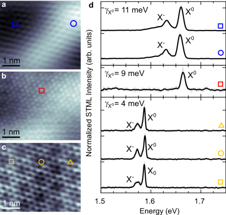
As a next step, we evaluate how the atomic-scale landscape affects excitonic emission from the MoSe2 monolayer. In Fig. 3a-c, we show atomically-resolved STM images of three distinct flat regions of the heterostructure, separated by several micrometres from one another. STML spectra (Fig. 3d) have been acquired in each region for tip positions marked by colored symbols in Fig. 3a-c. In Fig. 3a the STM image reveals the atomic structure of the TMD as well as bright and dark regions indicating smooth height modulation over several nanometres. Here, the STML spectra do not appear to be affected by these modulations, and are characterised by the typical and emission lines. In Fig. 3b and c, we distinguish a moiré pattern superimposed on the atomic structure, suggesting a better quality of the MoSe2/FLG interface than in Fig. 3a. This hypothesis is supported by the reduction of the excitonic linewidth from 11 meV (Fig. 3a) to 9 meV (Fig. 3b) and 4 meV (Fig. 3c), respectively. This linewidth narrowing can be assigned to reduced dephasing due to a more homogeneous environment. This higher quality interface may also lead to a more efficient static charge redistribution from the TMD to the FLG flake Lorchat et al. (2020); Hill et al. (2017), explaining the absence of trions in the STML spectrum acquired in Fig. 3b. Noteworthy, within a given nanoscale area, the STML spectra do not depend on the position of the tip with respect to the moiré pattern, as revealed in Fig. 3c.
However, in region (c) two emission lines, separated by only 20 meV appear. The most prominent line is strongly redshifted by 70 meV with respect to the line in region (a). Here, an interpretation in terms of defect-induced emission can be ruled out as no atomic defects are imaged in region (c) and we tentatively assign this line to a screened . Note that a small redshift of typically 10 meV has already been reported in TMD/monolayer graphene (1LG) and arises from the imperfect cancellation of two effects: screening-induced reduction of the electronic bandgap and of the exciton binding energy Lorchat et al. (2020); Raja et al. (2017). The unusually large shift of 70 meV observed here could arise from the excellent coupling between the MoSe2/FLG heterostructure and the Au(111) substrate, illustrated by the clear observation of a moiré pattern. This tightly coupled stack may favor charge transfer from Au(111) to the MoSe2 layer as well as charge localization assisted by the moiré superpotential, hence enabling trion formation. In keeping with this scenario, the faint line located only 20 meV below could arise from a strongly screened trion () with a binding energy reduced by about 10 meV and 5 meV, compared to a bare MoSe2 monolayer Ross et al. (2013) and to a MoSe2/1LG heterostructure Lorchat et al. (2020), respectively. In contrast, the absence of emission from trions in region (b) is likely a consequence of the partial decoupling between the coupled MoSe2/FLG heterostructure and the underlying Au(111) substrate, a situation that prevents substrate mediated charge transfer to MoSe2 and trion formation. The distinct signals reported for regions (a), (b) and (c) that enable atomically-resolved STM imaging, therefore hint towards a key role of the MoSe2/FLG and FLG/Au(111) interfaces.
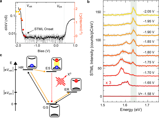
Finally, we jointly address the dependence of the tunnel current and STML spectra with the tip-sample bias at the same sample spot. The exciton binding energy, can in principle be estimated from the difference between the local electronic gap inferred from scanning tunnelling spectroscopy (STS) measurements and the optical gap determined from the energy. Figure 4a and b display a differential conductance () spectrum and set of STML spectra recorded with increasing bias voltage, respectively. An electronic gap of eV is deduced from the spectrum (see Supplementary Section 3 for details), with onsets of the valence and conductance bands at V and V respectively, indicating a weak doping. This doping allows us to identify the trion introduced in Fig. 1c and discussed in Fig. 2 and 3 as negatively charged. The STML spectra in Fig. 4b reveal an emission energy of 1.637 eV, leading to an energy difference of meV that is close to the value estimated by Ugeda et al. on a similar system using a combination of STS and PL Ugeda et al. (2014). This value is, however, much larger than state-of-the-art optical measurements of that converge towards values of 220 meV in hBN-capped monolayer MoSe2 Goryca et al. (2019) and 150 meV in monolayer MoSe2/1LG heterostructures Lorchat et al. (2020). Our data therefore demonstrate that the inconsistency between determinations of based on the difference between the STS gap and the optical gap versus all-optical measurements does not stem from spatial inhomogenities, as both electronic and optical measurements are local in our approach. We believe that this discrepancy rather originates from the fact that STS measurements poorly resolve electronic states with large in-plane momentum. This phenomenon ultimately leads to an overestimation of the electronic bandgap in STS studies since states near the point contribute more to the STS spectrum than those at the edges of the Brillouin zone ( and points), which define the direct electronic gap in TMD monolayers and from which wavefunctions are formed Zhang et al. (2015).
The comparison between STS and STML spectra provides key information regarding the STM-induced exciton formation mechanism. First, no STML signal could be observed under positive . Second, from Fig. 4b, one can deduce an emission onset at . Reporting the integrated intensity of the line as a function of in the spectrum (color-coded dots in Fig. 4a), one can see that the light emission onset matches well with the onset of the TMD electronic resonance, suggesting that hole injection from the tip is a preliminary step towards excitonic luminescence from the TMD. In Fig. 4c, we propose a simple scheme to explain the luminescence excitation mechanism. This scheme is inspired by a many-body approach developed to interpret STML data of molecules Miwa et al. (2019). Originally in its ground state (GS), the system can be approximated as a two-level system, where the low-energy level is occupied by an electron and the high energy one is empty. GS is here used as the origin of the energy scale on the left of the diagram. At a positive voltage 0.49 V, an electron can tunnel from the tip to the TMD (orange arrow) which is driven into a negatively charged (electron) resonance, denoted ER. This state is only transiently populated as the TMD can be efficiently driven back to GS by tunneling of the extra electron to the FLG/Au(111) substrate (black arrow). We can therefore associate the V feature in the spectrum of Fig. 4a to the GS ER transition. The same reasoning applies for a negative voltage of that corresponds to a transient positively charged (hole) resonance, denoted HR. Here, since , neutralization by electron transfer from the substrate can lead to the formation of an excited state (ES) in the MoSe2 monolayer that may rapidly relax as an optically active exciton (), whose radiative recombination (ES GS, red dotted line) is detected at 1.637 eV. Noteworthy, the STML line is accompanied by lower energy sideband, redshifted by about 40-50 meV and that we assign to STML from . In contrast to , the onset for emission occurs at (see Fig. 4b). As cannot be generated at this voltage, we deduce that are not generated from neutral excitons diffusing to defective areas of the sample, but instead formed directly at the tunneling junction. Their direct excitation may therefore involve in-gap localised electronic states of defects (not identified in the spectrum) or direct energy transfer from inelastic electrons. Further studies are needed to conclude on this point.
In conclusion, we have demonstrated STM-induced excitonic luminescence nanoscopy of an atomically-resolved van der Waals heterostructure. Our work directly reveals how the nanoscale environment influences the emission characteristics, leading to sizeable excitonic energy shifts and the emergence of emission features from charged and localised excitons on areas separated only by a few nanometres. Hyperspectral mapping of the STML response of atomically-resolved van der Waals heterostructures is still necessary to establish whether STM-induced luminescence imaging reaches sub-nanometre resolution in an extended 2D system, as it does in molecules Chen et al. (2010); Zhang et al. (2016); Doppagne et al. (2017); Doležal et al. (2021); Rosławska et al. (2022), or whether exciton diffusion Kulig et al. (2018) in TMD monolayers needs to be taken into account.
Further STML investigations could enable important advances in quantum materials science. First, STML offers exciting opportunities to unveil near-field charge and energy transfer Froehlicher et al. (2018); Bradac et al. (2021) and proximity effects Huang et al. (2020); Zutic et al. (2019) in vdW heterostructures with unprecedented accuracy, offering natural outcomes in photonics, opto-electronics and nano-electronics. Second, STML is an ideal tool to investigate correlated electronic phases Tang et al. (2020); Li et al. (2021); Wilson et al. (2021) and excitons in twist-engineered vdW heterostructures, starting with moiré-trapped interlayer excitons Seyler et al. (2019); Baek et al. (2020) and trions Liu et al. (2021) in TMD heterobilayers. Last but not least, STML can be combined with tip-enhanced photoluminescence spectroscopy Imada et al. (2021) to reach a holistic picture of exciton physics in van der Waals materials at the atomic scale.
Methods
Sample fabrication. The measurements were performed on a vdW heterostructure made using a dry transfer method described in Ref. Castellanos-Gomez et al., 2014. In brief, large-area monolayer MoSe2 and FLG were mechanically exfoliated from their bulk crystals on top of a thin film of polydimethylsiloxane (PDMS). This polymer is used as a temporary substrate in order to fabricate the vdW heterostructure. Its transparency allows for a precise alignment of the layers during the fabrication process. The FLG was then transferred onto a commercial Au(111) thin film grown on mica and the MoSe2 monolayer was afterwards stacked on top of it. The sample was then integrated onto a STM-compatible sample holder, allowing contacting the substrate from two sides (see Supplementary Section 1). The sample was annealed at C for 24 h under ultra-high vacuum to reduce surface contamination prior STM measurements.
PL characterization. The PL response of our sample was studied in vacuum ( mbar) at a temperature of 14 K in an optical cryostat coupled to a home-built confocal microscopy setup as in Ref. Lorchat et al., 2020. A linearly polarised continuous-wave laser beam at a wavelength of 532 nm (2.33 eV) with an intensity of 30 at the sample was used for all measurements. The PL signal was collected in a backscattering geometry and dispersed onto a liquid-nitrogen cooled CCD array using a 500 mm monochromator equipped with a 150 grooves/mm grating.
STM and STML measurements. STM-based measurements were performed in a low temperature (6 K) Unisoku STM operating in ultrahigh vacuum and adapted to optical measurements. A first lens (numerical aperture of 0.55), mounted on a three axis piezo controller, is used to collect and collimate the light emitted at the tip-sample junction. This light is then redirected outside of the vacuum chamber through successive windows and viewports. Afterwards, it is refocused on an optical fiber, itself connected to a spectrometer, and eventually detected using a nitrogen-cooled CCD camera. Three different gratings were used, yielding spectral resolutions ranging from 0.6 nm down to 0.06 nm. Silver (Ag) STM tips were used to optimise the plasmonic response of the junction and tested on a separate Ag(111) sample to maximise the radiative recombination rate at the tip-sample junction. The STS spectrum shown in Fig. 4a was acquired at constant height with a current setpoint pA and a modulation voltage mV.
Data analysis All PL and STML spectra presented in this work present both raw (light gray) and the smoothed data (solid colored line). Unless specified in the text, all spectra were fitted using Voigt profiles.
Acknowledgments
We thank Michael Chong, Benjamin Doppagne, Guillaume Froehlicher, Arnaud Gloppe, Eric Le Moal, Etienne Lorchat and Tomáš Neuman for fruitful discussions. We are grateful to the IPCMS mechanical workshop, in particular Halit Sumar, and Virginie Speisser, Michelangelo Romeo and the STnano clean room staff for technical support. This project has received funding from the European Research Council (ERC) under the European Union’s Horizon 2020 research and innovation program (grant agreement No 771850) and the European Union’s Horizon 2020 research and innovation program under the Marie Skłodowska-Curie grant agreement No 894434. We acknowledge financial support from the Agence Nationale de la Recherche under grant ATOEMS ANR-20-CE24-0010. This work of the Interdisciplinary Thematic Institute QMat, as part of the ITI 2021 2028 program of the University of Strasbourg, CNRS and Inserm, was supported by IdEx Unistra (ANR 10 IDEX 0002), and by SFRI STRAT’US project (ANR 20 SFRI 0012) and EUR QMAT ANR-17-EURE-0024 under the framework of the French Investments for the Future Program. S.B. acknowledges support from the Indo-French Centre for the Promotion of Advanced Research (CEFIPRA) and from the Institut Universitaire de France (IUF).
References
- Wang et al. (2018) Gang Wang, Alexey Chernikov, Mikhail M. Glazov, Tony F. Heinz, Xavier Marie, Thierry Amand, and Bernhard Urbaszek, “Colloquium: Excitons in atomically thin transition metal dichalcogenides,” Rev. Mod. Phys. 90, 021001 (2018).
- Mak and Shan (2016) Kin Fai Mak and Jie Shan, “Photonics and optoelectronics of 2D semiconductor transition metal dichalcogenides,” Nat. Photonics 10, 216–226 (2016).
- Wilson et al. (2021) Nathan P. Wilson, Wang Yao, Jie Shan, and Xiaodong Xu, “Excitons and emergent quantum phenomena in stacked 2D semiconductors,” Nature 599, 383–392 (2021).
- Shree et al. (2021) Shivangi Shree, Ioannis Paradisanos, Xavier Marie, Cedric Robert, and Bernhard Urbaszek, “Guide to optical spectroscopy of layered semiconductors,” Nature Reviews Physics 3, 39–54 (2021).
- Harats et al. (2020) Moshe G. Harats, Jan N. Kirchhof, Mengxiong Qiao, Kyrylo Greben, and Kirill I. Bolotin, “Dynamics and efficient conversion of excitons to trions in non-uniformly strained monolayer WS2,” Nature Photonics 14, 324–329 (2020).
- Raja et al. (2019) Archana Raja, Lutz Waldecker, Jonas Zipfel, Yeongsu Cho, Samuel Brem, Jonas D. Ziegler, Marvin Kulig, Takashi Taniguchi, Kenji Watanabe, Ermin Malic, Tony F. Heinz, Timothy C. Berkelbach, and Alexey Chernikov, “Dielectric disorder in two-dimensional materials,” Nature Nanotechnology 14, 832–837 (2019).
- Tongay et al. (2013a) Sefaattin Tongay, Joonki Suh, Can Ataca, Wen Fan, Alexander Luce, Jeong Seuk Kang, Jonathan Liu, Changhyun Ko, Rajamani Raghunathanan, Jian Zhou, Frank Ogletree, Jingbo Li, Jeffrey C. Grossman, and Junqiao Wu, “Defects activated photoluminescence in two-dimensional semiconductors: interplay between bound, charged and free excitons,” Scientific Reports 3, 2657 (2013a).
- Chow et al. (2015) Philippe K. Chow, Robin B. Jacobs-Gedrim, Jian Gao, Toh-Ming Lu, Bin Yu, Humberto Terrones, and Nikhil Koratkar, “Defect-induced photoluminescence in monolayer semiconducting transition metal dichalcogenides,” ACS Nano 9, 1520–1527 (2015).
- Tongay et al. (2013b) Sefaattin Tongay, Jian Zhou, Can Ataca, Jonathan Liu, Jeong Seuk Kang, Tyler S Matthews, Long You, Jingbo Li, Jeffrey C Grossman, and Junqiao Wu, “Broad-range modulation of light emission in two-dimensional semiconductors by molecular physisorption gating,” Nano Letters 13, 2831–2836 (2013b).
- Tang et al. (2020) Yanhao Tang, Lizhong Li, Tingxin Li, Yang Xu, Song Liu, Katayun Barmak, Kenji Watanabe, Takashi Taniguchi, Allan H. MacDonald, Jie Shan, and Kin Fai Mak, “Simulation of hubbard model physics in WSe2/WS2 moiré superlattices,” Nature 579, 353–358 (2020).
- Li et al. (2021) Hongyuan Li, Shaowei Li, Emma C. Regan, Danqing Wang, Wenyu Zhao, Salman Kahn, Kentaro Yumigeta, Mark Blei, Takashi Taniguchi, Kenji Watanabe, Sefaattin Tongay, Alex Zettl, Michael F. Crommie, and Feng Wang, “Imaging two-dimensional generalized wigner crystals,” Nature 597, 650–654 (2021).
- Kennes et al. (2021) Dante M. Kennes, Martin Claassen, Lede Xian, Antoine Georges, Andrew J. Millis, James Hone, Cory R. Dean, D. N. Basov, Abhay N. Pasupathy, and Angel Rubio, “Moiré heterostructures as a condensed-matter quantum simulator,” Nature Physics 17, 155–163 (2021).
- Yu et al. (2017) Hongyi Yu, Gui-Bin Liu, Jianju Tang, Xiaodong Xu, and Wang Yao, “Moiré excitons: From programmable quantum emitter arrays to spin-orbit-coupled artificial lattices,” Science Advances 3, e1701696 (2017).
- Huang et al. (2022) Di Huang, Junho Choi, Chih-Kang Shih, and Xiaoqin Li, “Excitons in semiconductor moiré superlattices,” Nature Nanotechnology 17, 227–238 (2022).
- Park et al. (2018) Kyoung-Duck Park, Tao Jiang, Genevieve Clark, Xiaodong Xu, and Markus B. Raschke, “Radiative control of dark excitons at room temperature by nano-optical antenna-tip purcell effect,” Nature Nanotechnology 13, 59–64 (2018).
- Darlington et al. (2020) Thomas P. Darlington, Christian Carmesin, Matthias Florian, Emanuil Yanev, Obafunso Ajayi, Jenny Ardelean, Daniel A. Rhodes, Augusto Ghiotto, Andrey Krayev, Kenji Watanabe, Takashi Taniguchi, Jeffrey W. Kysar, Abhay N. Pasupathy, James C. Hone, Frank Jahnke, Nicholas J. Borys, and P. James Schuck, “Imaging strain-localized excitons in nanoscale bubbles of monolayer WSe2 at room temperature,” Nature Nanotechnology 15, 854–860 (2020).
- Bonnet et al. (2021) Noémie Bonnet, Hae Yeon Lee, Fuhui Shao, Steffi Y. Woo, Jean-Denis Blazit, Kenji Watanabe, Takashi Taniguchi, Alberto Zobelli, Odile Stéphan, Mathieu Kociak, Silvija Gradecak, and Luiz H. G. Tizei, “Nanoscale modification of WS2 trion emission by its local electromagnetic environment,” Nano Letters 21, 10178–10185 (2021).
- Pommier et al. (2019) Delphine Pommier, Rémi Bretel, Luis E. Parra López, Florentin Fabre, Andrew Mayne, Elizabeth Boer-Duchemin, Gérald Dujardin, Guillaume Schull, Stéphane Berciaud, and Eric Le Moal, “Scanning tunneling microscope-induced excitonic luminescence of a two-dimensional semiconductor,” Physical Review Letters 123, 027402 (2019).
- Péchou et al. (2020) Renaud Péchou, Shuai Jia, Joel Rigor, Olivier Guillermet, Grégory Seine, Jun Lou, Nicolas Large, Adnen Mlayah, and Roland Coratger, “Plasmonic-induced luminescence of MoSe2 monolayers in a scanning tunneling microscope,” ACS photonics 7, 3061–3070 (2020).
- Peña Román et al. (2020) Ricardo Javier Peña Román, Yves Auad, Lucas Grasso, Fernando Alvarez, Ingrid David Barcelos, and Luiz Fernando Zagonel, “Tunneling-current-induced local excitonic luminescence in p-doped WSe2 monolayers,” Nanoscale 12, 13460–13470 (2020).
- Zhang et al. (2022) Shuai Zhang, Baichang Li, Xinzhong Chen, Francesco L. Ruta, Yinming Shao, Aaron J. Sternbach, A. S. McLeod, Zhiyuan Sun, Lin Xiong, S. L. Moore, Xinyi Xu, Wenjing Wu, Sara Shabani, Lin Zhou, Zhiying Wang, Fabian Mooshammer, Essance Ray, Nathan Wilson, P. J. Schuck, C. R. Dean, A. N. Pasupathy, Michal Lipson, Xiaodong Xu, Xiaoyang Zhu, A. J. Millis, Mengkun Liu, James C. Hone, and D. N. Basov, “Nano-spectroscopy of excitons in atomically thin transition metal dichalcogenides,” Nature Communications 13, 542 (2022).
- Qiu et al. (2003) X. H. Qiu, G. V. Nazin, and W. Ho, “Vibrationally resolved fluorescence excited with submolecular precision,” Science 299, 542–546 (2003).
- Wu et al. (2008) S. W. Wu, G. V. Nazin, and W. Ho, “Intramolecular photon emission from a single molecule in a scanning tunneling microscope,” Physical Review B 77, 205430 (2008).
- Zhang et al. (2016) Yang Zhang, Yang Luo, Yao Zhang, Yun-Jie Yu, Yan-Min Kuang, Li Zhang, Qiu-Shi Meng, Yi Luo, Jin-Long Yang, Zhen-Chao Dong, and J. G. Hou, “Visualizing coherent intermolecular dipole–dipole coupling in real space,” Nature 531, 623–627 (2016).
- Doppagne et al. (2017) Benjamin Doppagne, Michael C. Chong, Etienne Lorchat, Stéphane Berciaud, Michelangelo Romeo, Hervé Bulou, Alex Boeglin, Fabrice Scheurer, and Guillaume Schull, “Vibronic spectroscopy with submolecular resolution from STM-induced electroluminescence,” Physical Review Letters 118, 127401 (2017).
- Zhang et al. (2017a) Li Zhang, Yun-Jie Yu, Liu-Guo Chen, Yang Luo, Ben Yang, Fan-Fang Kong, Gong Chen, Yang Zhang, Qiang Zhang, Yi Luo, Jin-Long Yang, Zhen-Chao Dong, and J. G. Hou, “Electrically driven single-photon emission from an isolated single molecule,” Nature Communications 8, 580 (2017a).
- Doppagne et al. (2018) Benjamin Doppagne, Michael C. Chong, Hervé Bulou, Alex Boeglin, Fabrice Scheurer, and Guillaume Schull, “Electrofluorochromism at the single-molecule level,” Science 361, 251–255 (2018).
- Kimura et al. (2019) Kensuke Kimura, Kuniyuki Miwa, Hiroshi Imada, Miyabi Imai-Imada, Shota Kawahara, Jun Takeya, Maki Kawai, Michael Galperin, and Yousoo Kim, “Selective triplet exciton formation in a single molecule,” Nature 570, 210–213 (2019).
- Krane et al. (2016) Nils Krane, Christian Lotze, Julia M. Lager, Gaël Reecht, and Katharina J. Franke, “Electronic structure and luminescence of quasi-freestanding MoS2 nanopatches on Au(111),” Nano Letters 16, 5163–5168 (2016).
- Schuler et al. (2020) Bruno Schuler, Katherine A. Cochrane, Christoph Kastl, Edward S. Barnard, Edward Wong, Nicholas J. Borys, Adam M. Schwartzberg, D. Frank Ogletree, F. Javier García de Abajo, and Alexander Weber-Bargioni, “Electrically driven photon emission from individual atomic defects in monolayer WS2,” Science Advances 6, eabb5988 (2020).
- Velický et al. (2018) Matej Velický, Gavin E. Donnelly, William R. Hendren, Stephen McFarland, Declan Scullion, William J. I. DeBenedetti, Gabriela Calinao Correa, Yimo Han, Andrew J. Wain, Melissa A. Hines, David A. Muller, Kostya S. Novoselov, Héctor D. Abruña, Robert M. Bowman, Elton J. G. Santos, and Fumin Huang, “Mechanism of gold-assisted exfoliation of centimeter-sized transition-metal dichalcogenide monolayers,” ACS Nano 12, 10463–10472 (2018).
- Dean et al. (2010) C. R. Dean, A. F. Young, I. Meric, C. Lee, L. Wang, S. Sorgenfrei, K. Watanabe, T. Taniguchi, P. Kim, K. L. Shepard, and J. Hone, “Boron nitride substrates for high-quality graphene electronics,” Nature Nanotechnology 5, 722–726 (2010).
- Cadiz et al. (2017) F. Cadiz, E. Courtade, C. Robert, G. Wang, Y. Shen, H. Cai, T. Taniguchi, K. Watanabe, H. Carrere, D. Lagarde, M. Manca, T. Amand, P. Renucci, S. Tongay, X. Marie, and B. Urbaszek, “Excitonic linewidth approaching the homogeneous limit in MoS2-based van der Waals heterostructures,” Phys. Rev. X 7, 021026 (2017).
- Rosławska et al. (2022) Anna Rosławska, Tomáš Neuman, Benjamin Doppagne, Andrei G. Borisov, Michelangelo Romeo, Fabrice Scheurer, Javier Aizpurua, and Guillaume Schull, “Mapping Lamb, Stark, and Purcell effects at a chromophore-picocavity junction with hyper-resolved fluorescence microscopy,” Phys. Rev. X 12, 011012 (2022).
- Ross et al. (2013) Jason S. Ross, Sanfeng Wu, Hongyi Yu, Nirmal J. Ghimire, Aaron M. Jones, Grant Aivazian, Jiaqiang Yan, David G. Mandrus, Di Xiao, Wang Yao, and Xiaodong Xu, “Electrical control of neutral and charged excitons in a monolayer semiconductor,” Nature Communications 4, 1474 (2013).
- Wang et al. (2015) G. Wang, E. Palleau, T. Amand, S. Tongay, X. Marie, and B. Urbaszek, “Polarization and time-resolved photoluminescence spectroscopy of excitons in MoSe2 monolayers,” Applied Physics Letters 106, 112101 (2015).
- Branny et al. (2016) Artur Branny, Gang Wang, Santosh Kumar, Cedric Robert, Benjamin Lassagne, Xavier Marie, Brian D. Gerardot, and Bernhard Urbaszek, “Discrete quantum dot like emitters in monolayer MoSe2: Spatial mapping, magneto-optics, and charge tuning,” Applied Physics Letters 108, 142101 (2016).
- Lorchat et al. (2020) Etienne Lorchat, Luis E. Parra López, Cédric Robert, Delphine Lagarde, Guillaume Froehlicher, Takashi Taniguchi, Kenji Watanabe, Xavier Marie, and Stéphane Berciaud, “Filtering the photoluminescence spectra of atomically thin semiconductors with graphene,” Nature Nanotechnology 15, 283–288 (2020).
- Fang et al. (2019) H. H. Fang, B. Han, C. Robert, M. A. Semina, D. Lagarde, E. Courtade, T. Taniguchi, K. Watanabe, T. Amand, B. Urbaszek, M. M. Glazov, and X. Marie, “Control of the exciton radiative lifetime in van der Waals heterostructures,” Physical Review Letters 123, 067401 (2019).
- Robert et al. (2016) C. Robert, D. Lagarde, F. Cadiz, G. Wang, B. Lassagne, T. Amand, A. Balocchi, P. Renucci, S. Tongay, B. Urbaszek, and X. Marie, “Exciton radiative lifetime in transition metal dichalcogenide monolayers,” Physical Review B 93, 205423 (2016).
- Castellanos-Gomez et al. (2014) Andres Castellanos-Gomez, Michele Buscema, Rianda Molenaar, Vibhor Singh, Laurens Janssen, Herre S. J. van der Zant, and Gary A. Steele, “Deterministic transfer of two-dimensional materials by all-dry viscoelastic stamping,” 2D Materials 1, 011002 (2014).
- He et al. (2015) Yu-Ming He, Genevieve Clark, John R. Schaibley, Yu He, Ming-Cheng Chen, Yu-Jia Wei, Xing Ding, Qiang Zhang, Wang Yao, Xiaodong Xu, Chao-Yang Lu, and Jian-Wei Pan, “Single quantum emitters in monolayer semiconductors,” Nature Nanotechnology 10, 497–502 (2015).
- Chakraborty et al. (2015) Chitraleema Chakraborty, Laura Kinnischtzke, Kenneth M. Goodfellow, Ryan Beams, and A. Nick Vamivakas, “Voltage-controlled quantum light from an atomically thin semiconductor,” Nature Nanotechnology 10, 507–511 (2015).
- Koperski et al. (2015) M. Koperski, K. Nogajewski, A. Arora, V. Cherkez, P. Mallet, J.-Y. Veuillen, J. Marcus, P. Kossacki, and M. Potemski, “Single photon emitters in exfoliated WSe2 structures,” Nature Nanotechnology 10, 503–506 (2015).
- Srivastava et al. (2015) Ajit Srivastava, Meinrad Sidler, Adrien V Allain, Dominik S Lembke, Andras Kis, and Atac Imamoğlu, “Valley zeeman effect in elementary optical excitations of monolayer WSe2,” Nature Physics 11, 141 (2015).
- Tonndorf et al. (2015) Philipp Tonndorf, Robert Schmidt, Robert Schneider, Johannes Kern, Michele Buscema, Gary A. Steele, Andres Castellanos-Gomez, Herre S. J. van der Zant, Steffen Michaelis de Vasconcellos, and Rudolf Bratschitsch, “Single-photon emission from localized excitons in an atomically thin semiconductor,” Optica 2, 347–352 (2015).
- Aharonovich et al. (2016) Igor Aharonovich, Dirk Englund, and Milos Toth, “Solid-state single-photon emitters,” Nature Photonics 10, 631–641 (2016).
- Branny et al. (2017) Artur Branny, Santosh Kumar, Raphaël Proux, and Brian D. Gerardot, “Deterministic strain-induced arrays of quantum emitters in a two-dimensional semiconductor,” Nature Communications 8, 15053 (2017).
- Palacios-Berraquero et al. (2017) Carmen Palacios-Berraquero, Dhiren M. Kara, Alejandro R.-P. Montblanch, Matteo Barbone, Pawel Latawiec, Duhee Yoon, Anna K. Ott, Marko Loncar, Andrea C. Ferrari, and Mete Atatüre, “Large-scale quantum-emitter arrays in atomically thin semiconductors,” Nature Communications 8, 15093 (2017).
- Merino et al. (2015) P. Merino, C. Große, A. Rosławska, K. Kuhnke, and K. Kern, “Exciton dynamics of C60-based single-photon emitters explored by Hanbury Brown–Twiss scanning tunnelling microscopy,” Nature Communications 6, 8461 (2015).
- Zhang et al. (2017b) Li Zhang, Yun-Jie Yu, Liu-Guo Chen, Yang Luo, Ben Yang, Fan-Fang Kong, Gong Chen, Yang Zhang, Qiang Zhang, Yi Luo, Jin-Long Yang, Zhen-Chao Dong, and J. G. Hou, “Electrically driven single-photon emission from an isolated single molecule,” Nature Communications 8, 580 (2017b).
- Hill et al. (2017) Heather M. Hill, Albert F. Rigosi, Archana Raja, Alexey Chernikov, Cyrielle Roquelet, and Tony F. Heinz, “Exciton broadening in WS2/graphene heterostructures,” Physical Review B 96, 205401 (2017).
- Raja et al. (2017) Archana Raja, Andrey Chaves, Jaeeun Yu, Ghidewon Arefe, Heather M. Hill, Albert F. Rigosi, Timothy C. Berkelbach, Philipp Nagler, Christian Schüller, Tobias Korn, Colin Nuckolls, James Hone, Louis E. Brus, Tony F. Heinz, David R. Reichman, and Alexey Chernikov, “Coulomb engineering of the bandgap and excitons in two-dimensional materials,” Nature Communications 8, 15251 (2017).
- Ugeda et al. (2014) Miguel M. Ugeda, Aaron J. Bradley, Su-Fei Shi, Felipe H. da Jornada, Yi Zhang, Diana Y. Qiu, Wei Ruan, Sung-Kwan Mo, Zahid Hussain, Zhi-Xun Shen, Feng Wang, Steven G. Louie, and Michael F. Crommie, “Giant bandgap renormalization and excitonic effects in a monolayer transition metal dichalcogenide semiconductor,” Nature Materials 13, 1091–1095 (2014).
- Goryca et al. (2019) M. Goryca, J. Li, A. V. Stier, T. Taniguchi, K. Watanabe, E. Courtade, S. Shree, C. Robert, B. Urbaszek, X. Marie, and S. A. Crooker, “Revealing exciton masses and dielectric properties of monolayer semiconductors with high magnetic fields,” Nature Communications 10, 4172 (2019).
- Zhang et al. (2015) Chendong Zhang, Yuxuan Chen, Amber Johnson, Ming-Yang Li, Lain-Jong Li, Patrick C. Mende, Randall M. Feenstra, and Chih-Kang Shih, “Probing critical point energies of transition metal dichalcogenides: Surprising indirect gap of single layer WSe2,” Nano Letters 15, 6494–6500 (2015).
- Miwa et al. (2019) Kuniyuki Miwa, Hiroshi Imada, Miyabi Imai-Imada, Kensuke Kimura, Michael Galperin, and Yousoo Kim, “Many-body state description of single-molecule electroluminescence driven by a scanning tunneling microscope,” Nano Letters 19, 2803–2811 (2019).
- Chen et al. (2010) Chi Chen, Ping Chu, C. A. Bobisch, D. L. Mills, and W. Ho, “Viewing the interior of a single molecule: Vibronically resolved photon imaging at submolecular resolution,” Physical Review Letters 105, 217402 (2010).
- Doležal et al. (2021) J. Doležal, S. Canola, P. Merino, and M. Švec, “Exciton-trion conversion dynamics in a single molecule,” ACS Nano 15, 7694–7699 (2021).
- Kulig et al. (2018) Marvin Kulig, Jonas Zipfel, Philipp Nagler, Sofia Blanter, Christian Schüller, Tobias Korn, Nicola Paradiso, Mikhail M. Glazov, and Alexey Chernikov, “Exciton diffusion and halo effects in monolayer semiconductors,” Physical Review Letters 120, 207401 (2018).
- Froehlicher et al. (2018) Guillaume Froehlicher, Etienne Lorchat, and Stéphane Berciaud, “Charge versus energy transfer in atomically thin graphene-transition metal dichalcogenide van der Waals heterostructures,” Phys. Rev. X 8, 011007 (2018).
- Bradac et al. (2021) Carlo Bradac, Zai-Quan Xu, and Igor Aharonovich, “Quantum energy and charge transfer at two-dimensional interfaces,” Nano Letters 21, 1193–1204 (2021).
- Huang et al. (2020) Bevin Huang, Michael A. McGuire, Andrew F. May, Di Xiao, Pablo Jarillo-Herrero, and Xiaodong Xu, “Emergent phenomena and proximity effects in two-dimensional magnets and heterostructures,” Nature Materials 19, 1276–1289 (2020).
- Zutic et al. (2019) Igor Zutic, Alex Matos-Abiague, Benedikt Scharf, Hanan Dery, and Kirill Belashchenko, “Proximitized materials,” Materials Today 22, 85–107 (2019).
- Seyler et al. (2019) Kyle L. Seyler, Pasqual Rivera, Hongyi Yu, Nathan P. Wilson, Essance L. Ray, David G. Mandrus, Jiaqiang Yan, Wang Yao, and Xiaodong Xu, “Signatures of moiré-trapped valley excitons in MoSe2/WSe2 heterobilayers,” Nature 567, 66–70 (2019).
- Baek et al. (2020) H. Baek, M. Brotons-Gisbert, Z.X. Koong, A. Campbell, M. Rambach, K. Watanabe, T. Taniguchi, and B.D. Gerardot, “Highly energy-tunable quantum light from moiré-trapped excitons,” Science advances 6, eaba8526 (2020).
- Liu et al. (2021) Erfu Liu, Elyse Barré, Jeremiah van Baren, Matthew Wilson, Takashi Taniguchi, Kenji Watanabe, Yong-Tao Cui, Nathaniel M. Gabor, Tony F. Heinz, Yia-Chung Chang, and Chun Hung Lui, “Signatures of moiré trions in WSe2/MoSe2 heterobilayers,” Nature 594, 46–50 (2021).
- Imada et al. (2021) Hiroshi Imada, Miyabi Imai-Imada, Kuniyuki Miwa, Hidemasa Yamane, Takeshi Iwasa, Yusuke Tanaka, Naoyuki Toriumi, Kensuke Kimura, Nobuhiko Yokoshi, Atsuya Muranaka, Masanobu Uchiyama, Tetsuya Taketsugu, Yuichiro K. Kato, Hajime Ishihara, and Yousoo Kim, “Single-molecule laser nanospectroscopy with micro-electron volt energy resolution,” Science 373, 95–98 (2021).
- Grzeszczyk et al. (2020) M. Grzeszczyk, M. R. Molas, K. Nogajewski, M. Bartoš, A. Bogucki, C. Faugeras, P. Kossacki, A. Babiński, and M. Potemski, “The effect of metallic substrates on the optical properties of monolayer MoSe2,” Scientific Reports 10, 4981 (2020).
Supplementary Information for:
Tip-induced excitonic luminescence nanoscopy of an atomically-resolved van der Waals heterostructure
S1 Sample architecture
The sample consists of a monolayer of MoSe2 stacked on top of a few () layer graphene flake (FLG). The layers were isolated by mechanical exfoliation from bulk crystals and subsequent deposition onto polydimethylsiloxane (PDMS) films. After optical identification of individual layers, the stacking was performed in a homemade stamping station following the dry transfer method described in Ref. Castellanos-Gomez et al. (2014).To ensure compatibility with our STM setup, we used, as a substrate, a commercial thin Au(111) film grown on mica. An optical image of the sample is shown in Fig. S1a. Finally, the sample was integrated into a STM-compatible sample holder, which allows us to contact the substrate from two sides. The final configuration of the sample is shown in Fig. S1b.
S2 Micro-photoluminescence (PL) characterization at 14 K
Following the fabrication, the sample is rapidly introduced in a preparation chamber and annealed for 24 h at 200 under ultra high vacuum (UHV) conditions. Although this step is crucial to perform STM measurements, it can significantly modify the optical properties of the monolayer Lorchat et al. (2020); Peña Román et al. (2020). The rise in temperature enhances contaminant diffusion at the different interfaces, resulting in a spatially-dependent coupling between the component layers and between the heterostructure and the substrate itself. These variations would then modify nanoscale landscape and ultimately determine the optical properties of the heterostructure. At room temperature, it has been observed that the annealing of mechanically exfoliated TMD on Au(111) can lead to a drastic quenching of the PL and STML signals Peña Román et al. (2020). At cryogenic temperatures, a wide variety of spectra have been reported in TMD/Au heterostructures. From ”typical” spectra akin to the ones observed on monolayer TMD deposited onto non-metallic substrates, to spectra composed of multiple resonances and dominated by dielectric screening and quenching Grzeszczyk et al. (2020); Lorchat et al. (2020). In the case of extremely clean TMD/metal interfaces, such as the ones obtained using epitaxial growth, a complete quenching of the luminescence has been reported Krane et al. (2016); Schuler et al. (2020). This points towards the interface quality as the main driver of the optical properties of the heterostructure.
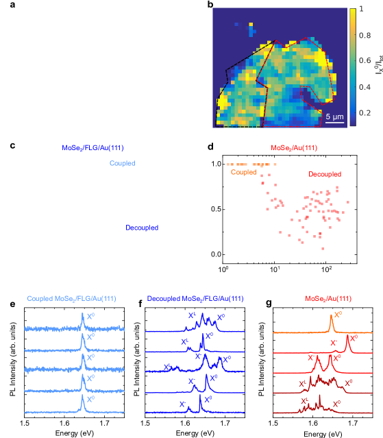
In our case, the self-cleaning mechanism clusters contaminants together at the MoSe2/FLG interface. This ensures the presence of locally contaminant-free areas as can be seen in Fig. 2a in the main text. As a result, the nanoscopic landscape of the sample is composed of different “patches” of homogeneous areas displaying varying degrees of coupling, strain and screening. This heterogeneity has a direct impact on the PL spectra, which spatially average excitonic recombination over a diffraction-limited area. Figure S2a shows a hyperspectral map of the total integrated PL intensity () of the MoSe2/FLG/Au(111) heterostructure. We observe PL signal variations of one order of magnitude between coupled (dim areas) and decoupled areas (bright areas) in both MoSe2/FLG/Au(111) and MoSe2/Au(111) surfaces. This is a direct signature of the local interface quality between the components. In the case of MoSe2/FLG, there are two interfaces that may play a role: the MoSe2/FLG interface regulating exciton transfer from MoSe2 to graphene and the FLG/Au(111) interface, which can further contribute to luminescence quenching and dielectric screening. We can illustrate this by plotting, in Fig. S2b, the ratio between the integrated intensity of the neutral exciton () emission () and . Qualitatively, We observe that the dimmest areas (low ) tend to display near unity ratios. To substantiate this observation, we have plotted the correlation between the observed ratio and for spectra taken from coupled and decoupled areas of the heterostructure (Fig. S2c-d). In both regions, MoSe2/FLG/Au(111) and MoSe2/Au(111), a correlation between large ratios and correspondingly low is revealed. This is consistent with a scenario where the layers that compose the heterostructure are well coupled and the emission arises solely from , as observed in samples encapsulated in hexagonal Boron Nitride (hBN) Lorchat et al. (2020). In inhomogeneous areas, the presence of contaminants and bubbles contributes to exciton localization, resulting in extrinsic, low energy features in the PL spectra, which reduce the overall ratio.
Typical PL spectra recorded on the positions marked in Fig. S2a are shown in Fig. S2e-g. The spectra are characteristic of the main areas of the sample (also summarised in Fig. 1d: coupled MoSe2/FLG/Au(111) (light blue), decoupled MoSe2/FLG/Au(111) (blue), coupled MoSe2/Au(111) (orange), decoupled MoSe2/Au(111) (red) and MoSe2/Au(111) in the vicinity of bubbles (dark red). In coupled areas (Fig. S2e and g), single-line PL spectra are observed, as previously reported in hBN-capped TMD/graphene heterostructures Lorchat et al. (2020). On the other hand, decoupled areas display multiple low-energy peaks arising from neutral, charged and localised excitons (, and respectively) as shown in Fig. S2f,g. The number of peaks and their positions are spatially dependent and are a direct signature of the homogeneity of the probed area. Nevertheless, one can recover ”typical” spectra composed of two peaks ( and ). Interestingly, we observe redshifts of the excitonic emission as large as 40 meV within decoupled regions (bottom spectra in Fig. S2f and red spectra in Fig S2g). We speculate that these redshifts are due to a combination of strain and screening from the Au(111) substrate.
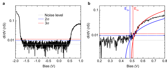
S3 Determination of the electronic gap
To determine the onset of the bands in the differential conductance spectra (see Fig. 4a in the main text), we used a similar procedure as in Ref. Ugeda et al., 2014. This procedure is illustrated in Fig. S3 and can be summarised as follows:
-
•
First, we plot the spectrum on a semi-logarithmic scale (Fig. S3a). A rigid vertical offset was applied to avoid running into negative values.
-
•
To estimate the noise level of the measured conductance, we compute the average value (gray dashed line in Fig. S3a) and the standard deviation of the noise inside the gap.
-
•
We defined two thresholds from which we consider that the signal is sufficiently different from the noise floor. These correspond to and ( being the standard deviation) above the average noise. These thresholds are represented by the blue and red dashed lines in Fig. S3a, respectively.
-
•
Finally, we used linear fits of the bands within a range of and with . was chosen so that the Pearson coefficient of the fits is not smaller than 0.95.
-
•
The onset of the bands is then defined as the intersection between the linear fit and the floor level for each threshold. We then calculate the average of both values.
-
•
These values are marked with the dashed vertical lines in Fig. S3b.
Using this procedure, we could determine an electronic gap of eV all over the sampled region.