Tunable nano-plasmonic photodetectors
I. Introduction
Active elements in modern integrated electronic circuits have reached sizes of only a few tens of nanometers [1], thanks to the short de Broglie wavelength of the conduction electrons. Optical elements, on the other hand, are limited by diffraction effects, leading to much larger device sizes typically beyond the scale of the photon wavelength [4, 11]. Yet it is desirable to integrate electronic and photonic elements, since light is widely employed as signal carrier in modern telecommunication applications [20]. This in particular includes photodetectors, which convert optical into electrical signals. However, shrinking photodetectors below the diffraction limit is not easily possible without loss in efficiency. First of all, reducing the thickness of the detector leads to decreasing light absorption in its active material [11]. This especially applies for silicon, due to its indirect bandgap, but also to other materials, like few-layer transition-metal dichalcogenides, which are promising for modern photonic applications and narrow-band photodetectors, due to their comparatively strong absorption at their exciton transition energies [27, 19]. Secondly, if the lateral size is reduced below the diffraction limit, the absorption in the device will decrease due to the mismatch between the detector cross section and the area of the incoming light field. Finally, electrical connections have to be attached to the active material, which can lead to shadowing of the detection-area, further reducing the device efficiency [8, 17].
All of these problems can be circumvented by employing electrically-connected plasmonic nanoantennas as light collecting elements, since they provide significant antenna gain, i.e. they channel light from an effective cross section that is larger than their geometrical footprint [22]. This leads to more efficient utilization of the incoming light even for small lateral sizes and at low thicknesses. In addition, the metallic antenna itself can be used as electrode, reducing the shadow effect imposed by electrical connections [8]. Also, plasmonic nanoantennas can be used directly as source of hot electrons and holes that are created inside the antenna material upon absorption of light [21]. By combining the antennas with a semiconducting material, these hot carriers will contribute to a photocurrent via the internal photoeffect (IPE). This approach has been used for photodetectors with a broadband response in the visible (VIS) and near infrared (NIR) regime [6, 24, 28], independent of the bandgap of the used semiconductor (SC), while the resonant behavior of plasmonic nanoantennas has allowed to selectively enhance the detection of a defined wavelength range, which can be tuned via the antenna geometry [12, 9, 16]. Moreover electronic responsivity switching [28] and polarization detection [9, 16] have been reported for plasmonic IPE detectors. However, to achieve reasonable photocurrents, large arrays of nanostructures had to be used so far [10].
Here we show that the IPE in a single nanoantenna device can be utilized for photodetection at the diffraction limit by combining electrically connected gold nanoantennas with titaniumoxide ( \chTiO_x ) as semiconducting material. This material stack allows a broadband VIS/NIR response while the antenna geometry determines the specific absorption wavelength. Further, we are able to electrically select this wavelength and determine the polarization angle of linearly polarized photons by employing different antenna geometries. Our results are promising for ultra-small photodetectors with potential application, e.g., in high-resolution laser beam profiling.
II. Results and discussion
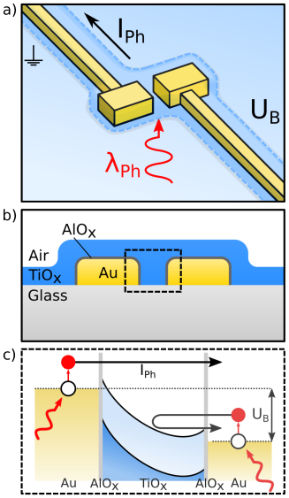
In the simplest case, our device consist of a single dimer antenna on a glass substrate, like shown in figure 1 a), electrically connected via two wires and coated with a semiconducting material to facilitate IPE. We structure the antenna from a mono-crystalline gold flake [15] via focused ion beam milling and conformally coat it with \chTiO_x in an atomic layer deposition process. The thickness of the \chTiO_x layer is chosen to fill the gap between the two arms of the antenna.
Since the direct growth of \chTiO_x on gold structures led to ohmic contacts, we introduced a thin interfacial layer of aluminumoxide (\chAlO_x) for interface passivation, which drastically lowers the dark current [7]. With this additional layer we observe a Schottky-Barrier (SB) of eV, determined from temperature dependent dark-current measurements.
Figure 1 c) shows the energy band diagram of the device with applied bias voltage . This metal-semiconductor-metal (MSM) structure features two SBs, one at each antenna arm, leading to low dark current at moderate bias (see SI).
Photocurrent measurements were performed with excitation-wavelengths between 500-900 nm, which cannot directly lift electrons above the bandgap within the \chTiO_x layer [3, 23]. However, hot carriers are excited within the metallic antenna arms and may be injected into the SC via the IPE [30]. Due to the separation of holes and electrons at the SB, the electron flow is directed outwards, so from gold to the SC, while the electrons are subsequently collected by the other antenna arm. Therefore, the photocurrent is a superposition of the contributions from both antenna-arms, with opposing current polarity, leading to a zero net-current for symmetric devices. But this symmetry can be broken by applying a bias Voltage , resulting in a detectable photocurrent.
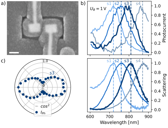
To proof the capability of this design to create very small photodetectors, we fabricated the symmetric dimer antenna displayed in the scanning electron micrograph (SEM) in figure 2 a) with a total length of 210 nm including the \chTiO_x layer. The size of the antenna is thus smaller than half of the shortest wavelength used during our measurements (500 nm).
The bright areas in the image correspond to the gold of our antenna while the light gray areas represent the \chTiO_x coating. The dark rectangular frame around the antenna is a trench resulting from the ion-milling process and does not have a significant influence on our measurements.
The photocurrent for this antenna was measured at =1 V with tunable monochromatic light from a supercontinuum laser (see SI). The resulting spectrum (s3 in figure 2 b) features a clear peak around 800 nm that agrees well with the resonance wavelength in the scattering measurement.
By changing the height and length of the antenna, the resonance can be precisely controlled over a wide spectral range, which is demonstrated by the four scattering spectra, from different antennas, featuring distinct peaks between 600-900 nm. Longer resonance wavelengths were achieved by increasing the aspect ratio of the antenna arms. The photocurrent peaks of all antennas coincide with the scattering resonances, showing that the color-selectivity of our detectors can be tuned via the antenna-dimensions.
The electrical connection wire also features a resonance in the scattering and photocurrent spectrum below 600 nm. This contribution is similar for all discussed antennas. For clarity, only the resonances of the dimers are shown. A full photocurrent spectrum can be found the in the SI.
The peaks in the photocurrent spectrum can be explained by the increased absorption at the plasmonic resonance, which results in a high rate of hot carriers around this spectral position [12]. This already shows that the antenna has a large influence on the properties of the detector. As a further consequence, the polarization pattern of the detector is defined by the antenna geometry as well. This is evident from the polarization dependent photoresponse depicted in figure 2 c), which can be approximately described by , with being the angle of polarization of the incident light relative to the antenna axis (x-direction in figure 2 a). The obtained two-lobed pattern, recorded at the resonance wavelength of the antenna, is characteristic for a dipolar antenna [22] and in agreement with previous reports [12]. Note that the data was corrected for a decay of the photocurrent over time. Details on this can be found in the SI.
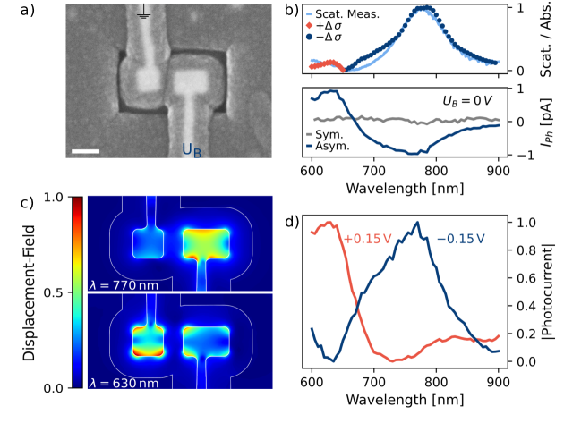
Besides the static tuning of the detector via the geometry, our concept also allows a dynamic switching of the color-response by applying a voltage. To this end, the asymmetric antenna in figure 3 a) is employed, which consist of two arms of different length, leading to two resonances in the device. While the longer arm contribution is clearly visible in the scattering spectra in figure 3 b), the short arm resonance is hardly visible due to its small size and the thus reduced scattering efficiency. We therefore performed FEM simulations, to prove the existence of the second resonance, taking the dimensions from the SEM image for our model. As seen from the displacement field plots in figure 3 c), the results indeed show two modes, at 630 nm and 770 nm respectively, with one antenna arm excited predominantly in either case.
As mentioned before, the photocurrent of a symmetric antenna is zero without applied bias voltage, which is visible in the gray curve in figure 3 b). However, for the case of the asymmetric dimer, both arms contribute currents with non-equal amplitude, depending on the excitation wavelength. For example at 630 nm, the short arm contributes more hot carriers as it is on resonance at this wavelength, while the long arm contributes more current at 770 nm. This leads to a non-zero net photocurrent with opposite polarity at the two resonances (see blue curve in the bottom plot of figure 3 b).
For comparison, we simulated the absorption in each arm separately, denoted as and , which is proportional to the hot carrier generation inside the respective arm. Therefore the difference resembles the net-photocurrent at zero bias. For comparability with the scattering, the absolute value is added to the top plot in figure 3 b), while the sign is color encoded. Although this simple model can predict the spectral positions of the peaks, it neglects important effects, like the wavelength dependent injection rate of hot carriers [12] or the scattering of hot carriers inside the metal [21]. To fully describe the photocurrent amplitude, a more extensive model is necessary, which is beyond the scope of this work.
To use the asymmetric antenna for dynamic color switching, a bias voltage is applied. This induces a potential barrier, which suppresses the hot carriers from one of the two arms [26, 28], as depicted in figure 1 c), reducing its contribution to the net current. This way, the carriers originating from the other antenna arm, on the higher electrical potential, are the main contributors to the photocurrent, and consequently, this arm defines the spectral response of the detector. Therefore, by switching the sign of , we can switch between the two resonances of the asymmetric antenna, which clearly changes the color response of the device (figure 3 d).
To completely suppress the photocurrent peak at a specific wavelength, the applied bias needs to be chosen carefully. The simulations in 3 c) show that at, say, 770 nm the excitation is spread over both arms, while one is clearly dominant. So, while the main part of the light is absorbed in the long arm, a small fraction is still absorbed in the short arm. Consequently, at sufficiently high bias, the short arm defines the photocurrent at 770 nm, although it is not at resonance, because the long rod´s hot electrons are blocked by the potential barrier. The optimal voltage, in our case , is therefore reached when the photocurrents of both arms cancel out at one resonance (the unwanted one). Choosing other values of can be used to tune the relative amplitude of the photocurrent peaks.
We now show that our plasmonic photodetector concept also allows to detect the polarization angle of linearly polarized light within a sub-diffractional device. The polarization pattern in figure 2 c) already shows that the photocurrent of the dimer antenna depends on , so, in principle, this can be used as a simple polarization detector already. If the power of the incoming light is constant and the angular dependence of the photocurrent is known, we can deduce the polarization angle by measuring . However, for the simple case of the dimer, depends on and . Thus, for variable , the polarization angle cannot be deduced from alone.
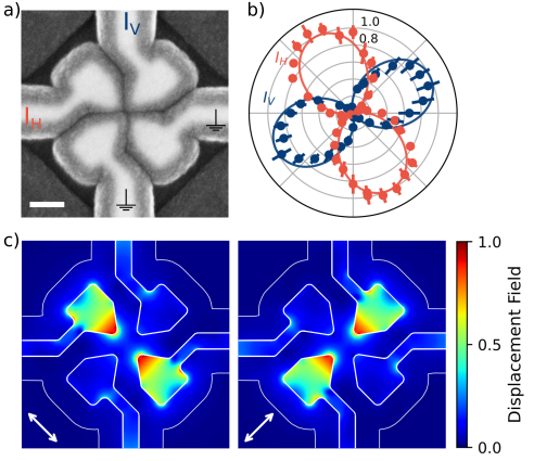
To overcome this problem, the antenna design depicted in figure 4 a) can be employed. This cross antenna consists of two dimers that are rotated by 90° with respect to each other [2], while the current through the antenna arms can be measured separately via the connection wires. The currents through the two dimers are denoted as and respectively (cf. figure 4 a). The resulting polarization patterns at the resonance wavelength are shown in figure 4 b). These two separate patterns can be described well by and respectively, which indicates an independent excitation of both dimers. The phase shift results from the overall rotation of the cross.
This independence is supported by FEM simulations for the cross antenna: The displacement-field plots in figure 4 c) were computed for two orthogonal polarization directions of the incoming light. In both cases the excitation of the dimer perpendicular to the polarization is negligible.
To measure we now use both photocurrents and , which again depend on the power of the incoming light and its polarization angle. However, the total current through the cross changes with power but does not depend on the polarization angle. Thus, by normalizing by , we arrive at a quantity that does depend on the polarization angle only, assuming that the amplitude of both photocurrent-patterns is the same for both dimers. Therefore, only needs to be measured once, at a constant light power, substantially reducing the necessary calibration effort for the cross antenna. As an experimental proof, we measured the polarization pattern for different powers of the excitation laser (see SI) and observed no significant changes in the normalized photocurrent, while the absolute values increased with higher powers. This shows that the cross antenna can be used as an intensity-invariant polarization detector.
Due to the four-fold symmetry, the cross antenna cannot uniquely resolve the angle of polarization. But this problem can be overcome by using an antenna with three-fold symmetry, like shown in the SI. The antenna presented there can resolve the polarization angle unambiguously, however at the cost of higher measurement complexity.
The antennas discussed in this work were fabricated to feature resonances in the range between 600-900 nm, which was limited by our excitation source, towards long wavelengths, and by the increasing absorption of gold below 600 nm. But in principle this wavelength range can be easily extended to the infrared by further increasing the aspect ratio of the antennas [22], in theory up to the SB height[12], which in our case is 1.0 eV. Plasmonic photodetectors at blue wavelengths are also feasible by employing different materials, like aluminum or silver [13].
A bigger limitation, in terms of possible applications, is the detection efficiency which is rather low compared to standard photodetectors based on silicon. We calculate the detection efficiency by dividing the photocurrent by the total incoming power of our laser light, corrected by the size of the laser spot and the antenna absorption cross section. See SI for details. With this we estimate an external quantum efficiency electrons per photon.
To a certain degree this efficiency is influenced by the thin \chAlO_x layer, but since it is comparable to other reports [12], the layer´s direct impact on seems to be rather insignificant, due to the small thickness of only 0.5 nm. More importantly, the injection of hot carriers into the semiconductor is believed to be the biggest limitation for plasmonic IPE detectors [21], although covering the antenna with the SC should slightly increase injection probability, compared to placing it on a flat SC surface [14].
In the future, this injection might be improved by the so-called "plasmon-induced interfacial charge-transfer transition", which features internal quantum efficiency of [29, 5, 18, 25]. Another approach to increase the detection efficiency could be via an integrated gain mechanism, like demonstrated for an IPE detector based on \chMoS2 with a reported photogain of [28].
In conclusion, we showed, that plasmonic IPE devices can be scaled down to a single antenna level, enabling detectors with sizes well below the wavelength of the detected light. In addition we demonstrated that these detectors can exhibit complex functionality like dynamic color switching and polarization detection, while keeping the small device footprint. This renders our concept promising for small scale photodetectors, especially for applications where high resolution demands are combined with high light intensity, like, for example, the profiling of focused laser beams.
References
- [1] International roadmap for devices and systems - more moore. Technical report, 2021.
- [2] Paolo Biagioni, Matteo Savoini, Jer-Shing Huang, Lamberto Duò, Marco Finazzi, and Bert Hecht. Near-field polarization shaping by a near-resonant plasmonic cross antenna. Physical Review B, 80(15), 2009.
- [3] Robert C. Devlin, Mohammadreza Khorasaninejad, Wei Ting Chen, Jaewon Oh, and Federico Capasso. Broadband high-efficiency dielectric metasurfaces for the visible spectrum. Proceedings of the National Academy of Sciences, 113(38):10473–10478, 2016.
- [4] E. R. Fossum and D. B. Hondongwa. A review of the pinned photodiode for CCD and CMOS image sensors. IEEE Journal of the Electron Devices Society, 2(3):33–43, 2014.
- [5] Akihiro Furube, Luchao Du, Kohjiro Hara, Ryuzi Katoh, and Masanori Tachiya. Ultrafast plasmon-induced electron transfer from gold nanodots into TiO nanoparticles. Journal of the American Chemical Society, 129(48):14852–14853, 2007.
- [6] Xu Dong Gao, Guang Tao Fei, Shao Hui Xu, Bin Nian Zhong, Hao Miao Ouyang, Xin Hua Li, and Li De Zhang. Porous ag/TiO2-schottky-diode based plasmonic hot-electron photodetector with high detectivity and fast response. Nanophotonics, 8(7):1247–1254, 2019.
- [7] F. Pelayo García de Arquer, Agustín Mihi, and Gerasimos Konstantatos. Large-area plasmonic-crystal–hot-electron-based photodetectors. ACS Photonics, 2(7):950–957, 2015.
- [8] J. Hetterich, G. Bastian, N. A. Gippius, S. G. Tikhodeev, G. von Plessen, and U. Lemmer. Optimized design of plasmonic MSM photodetector. IEEE Journal of Quantum Electronics, 43(10):855–859, 2007.
- [9] Y. Hou, H. Liang, A. Tang, X. Du, and Z. Mei. Hot-electron photocurrent detection of near-infrared light based on ZnO. Applied Physics Letters, 118(6):063501, 2021.
- [10] Jian-An Huang and Lin-Bao Luo. Low-dimensional plasmonic photodetectors: Recent progress and future opportunities. Advanced Optical Materials, 6(8):1701282, 2018.
- [11] HyunChul Kim, Jongeun Park, Insung Joe, Doowon Kwon, Joo Hyoung Kim, Dongsuk Cho, Taehun Lee, Changkyu Lee, Haeyong Park, Soojin Hong, Chongkwang Chang, Jingyun Kim, Hanjin Lim, Youngsun Oh, Yitae Kim, Seungjoo Nah, Sangill Jung, Jaekyu Lee, JungChak Ahn, Hyeongsun Hong, Kyupil Lee, and Ho-Kyu Kang. A 1/2.65in 44mpixel CMOS image sensor with 0.7µm pixels fabricated in advanced full-depth deep-trench isolation technology. In 2020 IEEE International Solid- State Circuits Conference - (ISSCC), pages 104–106, 2020.
- [12] M. W. Knight, H. Sobhani, P. Nordlander, and N. J. Halas. Photodetection with active optical antennas. Science, 332(6030):702–704, 2011.
- [13] Mark W. Knight, Nicholas S. King, Lifei Liu, Henry O. Everitt, Peter Nordlander, and Naomi J. Halas. Aluminum for plasmonics. ACS Nano, 8(1):834–840, 2014.
- [14] Mark W. Knight, Yumin Wang, Alexander S. Urban, Ali Sobhani, Bob Y. Zheng, Peter Nordlander, and Naomi J. Halas. Embedding plasmonic nanostructure diodes enhances hot electron emission. Nano Letters, 13(4):1687–1692, 2013.
- [15] Enno Krauss, René Kullock, Xiaofei Wu, Peter Geisler, Nils Lundt, Martin Kamp, and Bert Hecht. Controlled growth of high-aspect-ratio single-crystalline gold platelets. Crystal Growth & Design, 18(3):1297–1302, 2018.
- [16] Wei Li, J. Zachary Coppens, Lucas V. Besteiro, Wenyi Wang, O. Alexander Govorov, and Jason Valentine. Circularly polarized light detection with hot electrons in chiral plasmonic metamaterials. Nature Communications, page 7, 2015.
- [17] Chu-Hsuan Lin and Chee Wee Liu. Metal-insulator-semiconductor photodetectors. Sensors, 10(10):8797–8826, 2010.
- [18] Run Long and Oleg V Prezhdo. Instantaneous generation of charge-separated state on TiO2 surface sensitized with plasmonic nanoparticles. Journal of the American Chemical Society, 136(11):4343–4354, 2014.
- [19] Kin Fai Mak and Jie Shan. Photonics and optoelectronics of 2d semiconductor transition metal dichalcogenides. Nature Photonics, 10(4):216–226, 2016.
- [20] Fedor Mitschke. Fiber Optics: Physics and Technology. Springer Berlin Heidelberg, 2nd ed. 2016 edition, 2016.
- [21] Prineha Narang, Ravishankar Sundararaman, and Harry A. Atwater. Plasmonic hot carrier dynamics in solid-state and chemical systems for energy conversion. Nanophotonics, 5(1):96–111, 2016.
- [22] Lukas Novotny and Bert Hecht. Principles of Nano-Optics. Cambridge University Press, 2 edition, 2012.
- [23] J. Pascual, J. Camassel, and H. Mathieu. Fine structure in the intrinsic absorption edge of \chTiO2. Physical Review B, 18(10):5606–5614, 1978.
- [24] Giulia Tagliabue, Joseph S. DuChene, Adela Habib, Ravishankar Sundararaman, and Harry A. Atwater. Hot-hole versus hot-electron transport at cu/GaN heterojunction interfaces. ACS Nano, 14(5):5788–5797, 2020.
- [25] Shijing Tan, Adam Argondizzo, Jindong Ren, Liming Liu, Jin Zhao, and Hrvoje Petek. Plasmonic coupling at a metal/semiconductor interface. Nature Photonics, 11(12):806–812, 2017.
- [26] Fuming Wang and Nicholas A. Melosh. Power-independent wavelength determination by hot carrier collection in metal-insulator-metal devices. Nature Communications, 4(1):1711, 2013.
- [27] Qing Hua Wang, Kourosh Kalantar-Zadeh, Andras Kis, Jonathan N. Coleman, and Michael S. Strano. Electronics and optoelectronics of two-dimensional transition metal dichalcogenides. Nature Nanotechnology, 7(11):699–712, 2012.
- [28] Wenyi Wang, Andrey Klots, Dhiraj Prasai, Yuanmu Yang, Kirill I. Bolotin, and Jason Valentine. Hot electron-based near-infrared photodetection using bilayer \chMoS2. Nano Letters, 15(11):7440–7444, 2015.
- [29] K. Wu, J. Chen, J. R. McBride, and T. Lian. Efficient hot-electron transfer by a plasmon-induced interfacial charge-transfer transition. Science, 349(6248):632–635, 2015.
- [30] Bob Y. Zheng, Hangqi Zhao, Alejandro Manjavacas, Michael McClain, Peter Nordlander, and Naomi J. Halas. Distinguishing between plasmon-induced and photoexcited carriers in a device geometry. Nature Communications, 6(1):7797, 2015.