contributed equally to this paper
Infrared nanoplasmonic properties of hyperdoped embedded Si nanocrystals in the few electrons regime
Abstract
Using Localized Surface Plasmon Resonance (LSPR) as an optical probe we demonstrate the presence of free carriers in phosphorus doped silicon nanocrystals (SiNCs) embedded in a silica matrix. In small SiNCs, with radius ranging from 2.6 to 5.5 nm, the infrared spectroscopy study coupled to numerical simulations allows us to determine the number of electrically active phosphorus atoms with a precision of a few atoms. We demonstrate that LSP resonances can be supported with only about 10 free electrons per nanocrystal, confirming theoretical predictions and probing the limit of the collective nature of plasmons. We reveal a phenomenon, unique to embedded nanocrystals, with the appearance of an avoided crossing behavior linked to the hybridization between the localized surface plasmon in the doped nanocrystals and the silica matrix phonon modes. Finally, a careful analysis of the scattering time dependence versus carrier density in the small size regime allows us to detect the appearance of a new scattering process at high dopant concentration.
keywords:
Hyper doped silicium, Localized Surface Plasmon ResonanceLocalized surface plasmon resonances (LSPR), the collective oscillations of free carriers at metal surfaces, have been studied for decades due to their ability to fundamentally alter light-matter interactions and the resulting remarkable applications in: enhanced spectroscopy 1, sensing 2, optical devices, and photovoltaics 3. For a long time, plasmonics-based technology relied heavily on noble metal nanostructures due to their intense LSPR in the visible range 4. Things have begun to change recently, with the observation of LSPR in doped semiconductors. The new form of control provided by the tunability of carrier density in semiconductors, combined with the resulting expansion of plasmonics into the Infrared spectral range (not easily reached with metals), has fueled the search for novel plasmonic materials with improved crystalline quality, integrability, tunability, and potentially lower losses 5, 6.
However the real paradigm shift came with the observation of LSPR in very small semiconducting nanostructures and nanocrystals 7, 8, 9, 10, 11. Because the LSPR frequency becomes more sensitive to changes in the number of free carriers as the size of the nanocrystal decreases, with electro-optic sensitivity going as (r being the radius of the NC), it is possible to detect the addition of a very small number of carriers to a nanocrystal. In this context, LSPRs have emerged as an optical probe (contactless) with unprecedented sensitivity to processes involving carrier dynamics, that would otherwise be difficult to access. Furthermore, the concept of plasmon supported by a small number of carriers raises fundamental questions that go beyond material science issues, such as the minimum number of charge carriers required to sustain a plasmon resonance, the effect of confinement on the plasmon resonance, and the validity of the Drude model in such conditions.
In this article we investigate the plasmonic properties of phosphorus-doped Si nanocrystals (SiNCs) embedded in SiO2. We demonstrate that SiNCs can be massively doped by combining Low Energy Ion Implantation and Rapid Thermal Annealing (RTA), with measured LSPR wavelength ranging from 4 to 7 m depending on the P implantation dose. To determine the carrier density and electronic scattering time for all experimental doses, we use homemade numerical simulations based on the Green Dyadic Method (GDM), taking into account the complex multilayered dielectric environment of our samples. The simulation allowed us to put into light an hybridization between the LSPR and the optical phonon modes of the silica matrix. We were able to determine the variation of the phosphorus activation rate and pinpoint a lower limit to the number of activated carriers required to support plasmonic resonances by combining these results with atomically resolved 3D mapping. Finally, we demonstrate three distinct phenomena that drive the electronic scattering processes in SiNCs.
1 Results.
1.1 SiNCs fabrication and doping.
A 200 nm thick thermal silica layer on top of a silicon substrate is implanted with Si ions at an energy of 8 keV and a dose of 21016 cm-2. An intermediate RTA is performed for 60 seconds at 1050oC in N2 with the goal of phase separation and SiNCs formation. After the synthesis of SiNCs, dopant impurities are introduced into the SiNCs to decouple equilibrium properties from kinetic effects 12. Phosphorus is implanted in 5 doses at 7 keV to match the projected Si range. The ratio of the P and Si doses ranges from 5 to 15 . Following P implantation, the samples undergo a new annealing at 1050oC for 60 seconds dedicated to dopant activation. As a last step, a forming gas (FG) annealing at N2+10 H2 was used to passivate dangling bonds at the SiNCs/matrix interface 13.
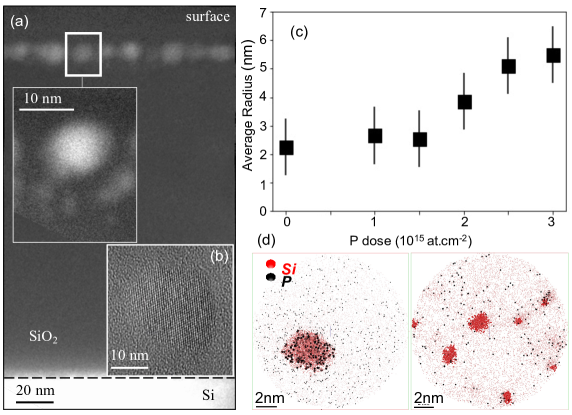
Figure 1(a) shows a low magnification Energy Filtered TEM (EFTEM) image of the SiNCs after doping. They are distributed along a 20 nm-thick band located at 4 nm from the surface. The doped SiNCs show a sharp and bimodal size distribution (see SI Fig. S1), with the largest SiNCs located at the profile projected range (15 nm) and small NCs located deeper in the profile tail. Figure 1(b) a high resolution image clearly shows that the doped SiNCs are spherical and remain crystalline after doping, with the same lattice parameter as bulk Si. At doses up to 1.51015 cm-2, the average NC diameter remains constant for both small (2.8 nm) NCs located in the profile tail and large (5 nm) NCs formed at the maximum of the implantation profile. On the contrary, at higher doses, the average diameter of the big NCs increases with the P dose, reaching up to twice the size of the low dose regime (see Fig. 1(c)). The increase in P concentration has no effect on the size of the small SiNCs. This enhanced NC growth with P concentration has previously been observed in the literature for SiNCs in a silica matrix prepared using various techniques 14, 15, 16. The hypothesis of P doping softening silica matrices has been proposed, resulting in longer diffusion length of Si atoms during annealing, and larger particles 16. Enhanced diffusion by implanted P atoms has also been proposed as a possible explanation for the favored SiNCs phase separation in the presence of P 14. A careful examination of atomically resolved 3D images obtained by laser-assisted Atom Probe Tomogrphy (ATP), shown in Figure 1(d) reveals the precise location of the dopant. The majority of P atoms, black dots on the figure, are well-concentrated inside the big SiNCs (see left panel), with a homogeneous distribution and no accumulation of dopant at the surface. These findings, are consistent with theoretical calculations 17, 18 and previous observations for similar systems 19, 20, 21. The position of P in the core of the SiNCs contradicts self-purification theories but is consistent with the well-known macroscopic behavior of these dopants at bulk Si/SiO2 interfaces, where segregation is in favor of silicon for phosphorus at thermal equilibrium 22. Small NCs contain very few, if no, P atoms, which is not surprising as they are located deeper inside the SiO2 matrix in the profile tail of the P implantation profile (see right panel Fig. 1(d)).
Scanning Transmission Electron Microscopy-Energy Dispersive X-Ray Spectroscopy (STEM-EDX) was used to determine the P content of SiNCs. The phosphorus Cliff-Lorimer coefficient has been quantitatively calibrated on a reference sample (P implantation in bulk Si) 23 . The P concentration in big SiNCs ranges from 3.2 to 6.3 1021 cm-3 (see Fig. 4(b)), whereas it is negligible and close to the detection limit in the small SiNCs and in the matrix. The high P concentration of the large SiNCs is consistent with previous studies 19, 24, 20 that conclude that doping SiNCs in SiO2 corresponds to a thermodynamically advantageous configuration. The measured P concentrations are up to 6 times higher than the solid solubility of P in bulk silicon at 1050oC (1021 cm-3) 25, implying that solubility in Si nanostructures has increased. 24, 20
1.2 SiNCs Plasmonic properties.
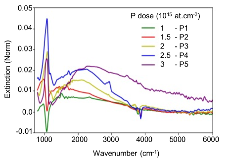
To determine the effect of the implanted phosphorus on the electronic properties of the SiNCs we performed Fourier Transform Infrared (FTIR) Spectroscopy at room temperature, in vacuum. This technique is an all-optical, non destructive and very sensitive method for active dopant concentration measurement in semiconductor bulk and nanostructures 6. Figure 2 shows the normalized extinction spectra recorded for the different implanted doses (P1 to P5). T. The extinction spectra are normalized using undoped SiNCs (P0) sample as a reference. This normalization procedure reduces the optical signature of the thermal silica layer as well as the likelihood of seeing interference patterns in the spectra. Two interesting features can be noticed in all five extinction curves: (i) A relatively sharp feature that appears at low frequency (around 1050 cm-1) and can be attributed to the multiple SiO2 phonon modes that are not completely removed by normalization 26, 27. (ii) A broad peak that shifts progressively higher in frequency as the P dose, thus the free carrier density, increases. This maximum of extinction is most likely related to the excitation of a localized surface plasmon in doped SiNCs. The amplitude of the plasmon mode is quite small, as expected for such small NC, reaching 2 for the highest dose (P5) and falling to 0.5 for the lowest dose (P1). Nonetheless, it is plainly visible.
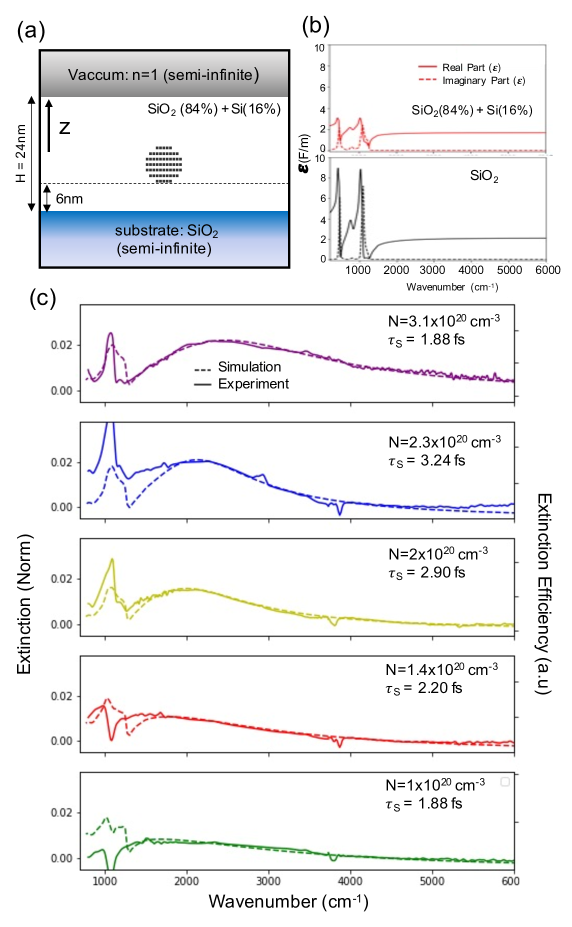
To confirm the plasmonic nature of the observed modification of extinction we model our experimental results using numerical simulations based on the Green Dyadic Method (GDM) with our homemade simulation toolkit “pyGDM” 28, 29. This method, which is based on nanostructure volume discretization, allows us to simulate the complex multilayered geometry of our samples, as shown in Figure 1(a). Figure 3 (a) depicts a schematic of the simulated geometry, with the NC represented by a doped silicon sphere. The Drude-Lorentz model is used to describe the dielectric function of the doped Si layer:
| (1) |
where = the Drude weight, is the electronic scattering rate and the dielectric function of intrinsic Si taken from Ref 30. In this expression, is the electron effective mass in Si, the elementary charge, the free carrier concentration. For each P dose the radius of the sphere is chosen to be the average radius of the large SiNCs (Figure 1(c)) in the bimodal size-distribution (see supplementary information, Figure S1). The doped Si sphere is then placed inside a 24 nm thick silicon rich SiO2 layer. The small NCs contained in this layer are undoped and thus do not contribute directly to the observed plasmonic properties, nevertheless they are made of pure silicon and present a dielectric function drastically different from the rest of the silica matrix. To accurately describe the complex dielectric environment of this layer we use the Maxwell Garnett mixing formula. It has been developed to approximate a complex electromagnetic medium such as a colloidal solution of gold micro-particles and gives an effective permittivity in terms of the permittivities and volume fractions of the individual constituents of the complex medium 31, 32:
| (2) |
With f the volume fraction of Si inclusions. In our calculation we fix f to 16, based on STEM-EDX measurement, the resulting dielectric function is displayed in Figure 3(b) (top panel). Finally this layer is sandwiched between a SiO2 substrate (see dielectric function in Figure 3(b) (bottom panel) and a vacuum cladding. The extinction efficiencies of individual doped SiNC in the simulated environment are then calculated using the Lippmann-Schwinger equation.
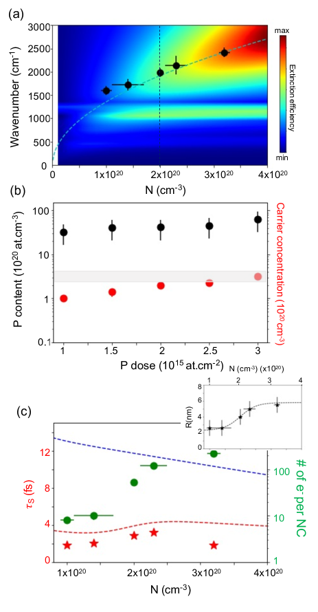
Figure 3(c) depicts the best fit we obtained for all P implanted doses. Note that as we calculate the extinction of one single NC, the simulation is not expected to reproduce the extinction absolute amplitude. All simulated curves in Figure 3(c) are by consequence normalized to the experimental LSPR amplitude. The fitting parameters are the carrier density and scattering time , with all other parameters held constant. For all samples, the simulated extinctions reproduce the LSPR signature very well. The theoretical description of the phonon-related extinction is satisfactory but not perfect. This result is not entirely unexpected given that the Maxwell Garnett model we used to simulate the Si rich silica layer (see equation 2) assumes isotropic composites i.e. with equivalent nanoparticle densities in all directions in space equivalent. However the undoped SiNCs inside the silica matrix are not uniformly distributed around the doped NC (see inset Figure 1 (a)). Nevertheless, the quality of the fitting procedure is a strong indication that the approximation is quite good (as a reference Figure S3 in supplementary shows the same simulations using ).
Figure 4 (a) depicts the maximum of extinction versus (black dots) extracted from Figure 3(c). As a reference, we plot in dashed line, on the same graph, the expected LSPR energy (Mie resonance) for a spherical NC 35:
| (3) |
where , the average dielectric function of the surrounding environment, is taken to be = 2.3 far from any phonon mode. One can see that at high carrier density the experimental points follow the expected square root dependence for plasmon resonances, but start deviating from it at low carrier density. To understand this discrepancy we calculated the frequency dependent extinction versus carrier density with a constant sphere radius of nm and constant scattering time fs, shown as the superimposed color map on the figure. This simulation indicates clearly that this deviation is mainly due to a hybridization between phonons of silica and the LSPR resulting in an avoided crossing 36, 37. The very good description of the experimental results we obtained here, while using a single value of NC’s radius ( nm) for all carrier densities, discard possible explanations linked to the NC’s size, in agreement with theoretical prediction that estimate that no quantization effects should be observed for Si-NCs with 38. Using the carrier density and average volume of the NC in our samples, we can calculate the average number of electrons (equal to the number of activated P atoms) in each NC contributing to the plasmon resonances. We deduced these values with a precision of few electrons and they range from more than 100 electrons for larger NCs (higher P dose) down to approximately ten electrons for small NCs (lower P dose, see green circles in Fig. 4(c)). Due to the collective nature of the plasmonic resonance the question of the minimum number of required electrons is of fundamental nature, our work is confirming the theoretical prediction made in 38 that estimated a minimum of 10 electrons for the plasmonic mode to emerge. This value is quite similar to what has been observed in metallic clusters (Hg) which display plasmon-like features with 11 electrons. 39 To go further and evaluate the potential of these systems as IR plasmonic materials, we provide in SI a detailed evaluation of the achievable GPI in these systems (see Figure S5). 40
It is worth noting here that the degree of optical field confinement (where is the SiNC diameter and the optical index of ) observed in those samples is extremely high, ranging from 250 for P5 up to 800 for P1. This is significantly higher than what can be obtained with noble metals and even better than what has previously been observed in hyper doped Si based plasmonic metasurfaces 6.
In Figure 4(b) the carrier density (red circles) is plotted as a function of the P implanted dose. One can clearly see that this value reaches the electrical solubility of P in bulk Si at C (grey rectangle) 33. Beyond this value, the additional P atoms likely form small electrically inactive clusters. The activation rate, defined as the ratio of the carrier density to the total number of P atoms inserted inside the SiNCs measured in STEM-EDX ranges between 3 and 5 . This activation ratio is more than one to two orders of magnitude higher than that previously measured on freestanding 41 or silica embedded 42 P doped SiNCs of the same size. However, this activation efficiency is lower than that measured on Si nanostructures obtained through top down processing of hyperdoped Si overlayers, where the activation process occurs at the bulk state and is optimized by non-equilibrium melt laser annealing 6.
Figure 4 (c) shows the scattering time versus the extracted carrier density. For similar carrier density, the scattering time observed in SiNCs (red stars in Figure 4(c)) is smaller than that observed in continuous Si layers (blue dashed line extracted from 34). Furthermore, (N) exhibits a non-monotonic dependence, increasing with at low density and decreasing at high density. To explain both observations, we must consider the effects of NC size on scattering time. As the diameter of the NC becomes smaller than the electron mean free path, electrons collide with the spherical NC surface at an average rate of , where is the Fermi velocity in Si 43. To account for the observed dependence of , we must consider two competing effects: (i) In silicon (bulk), the scattering time decreases with increasing carrier density, as described in Ref34 (see dashed blue line on figure 4(c)), (ii) the size of the NC in our system is a function of the P content and therefore of the carrier density, with an increasing function displayed in inset of Figure 4 (c). As a result, the effective collision time is N dependent 44:
| (4) |
with . The resulting is plotted as a red dashed line in Figure 4(c), and it accurately describes both the absolute values and the variation of the measured scattering time without the use of any adjusting parameters. It is now interesting to note that exhibits a larger deviation from the predicted behavior. For this sample the inactive dopant concentration (difference between the total P concentration measured by STEM-EDX and the carrier density measured by FTIR), is multiplied by 1.5 (see supplementary Fig. S4). Hence, more and more of the implanted phosphorus begins aggregating and forms electrically inactive clusters of a few atoms, degrading the electronic scattering rate inside the SiNCs.
In conclusion, we achieved massively doped SiNCs embedded in a silica matrix by combining Low Energy Ion Implantation and Rapid Thermal Annealing. We demonstrated that such embedded nanostructures can support localized surface plasmon resonances that are controlled by the silicon free carrier density. Despite a significant mismatch between the wavelength (4-7 m) and the Si-NC diameter (nm), the LSPR allows a strong interaction with IR light, resulting in an increase in extinction of up to 2 at the resonance. We investigated the optical properties of a single nanocrystal in a complex dielectric environment using numerical simulations. We observed a deviation from the expected square root dependance of the LSPR with the carrier density that we attributed to a coupling between the plasmon mode and the infrared phonons of the surrounding silica matrix. We demonstrated that 10 free electrons inside NC are sufficient to produce LSPR. Finally, because the diameter of our NC is smaller than the electron mean free path, we show that the scattering time dependence with carrier density in such NCs differs significantly from what is observed in bulk or larger Si nanostructures, and we were able to detect evidence of P aggregate formation.
2 Methods
2.0.1 Thermal Annealing
Rapid Thermal Annealing was carried out in a nitrogen atmosphere at a temperature of 1050o for 60 seconds. Halogen lamps allow to reach the targeted temperature with a speed of 20 oC/s for up, and 10 oC/s for down ramps. Forming gas annealing has been done using a H2/N2 mixture. This annealing process is dedicated to the passivation of the interface states between SiNCs and silica matrix . In this work, forming gas annealing using an RTA furnace was performed on pieces of samples at 500 o for 900 seconds with a gas mixture of 10 H2 + 90 N2.
2.0.2 Simulations
The Green Dyadic Method (GDM) is based on a volume discretization of the nanostructure and numerical solving of Maxwell’s equations in the frequency domain. From the Lippmann-Schwinger equation:
| (5) |
the time Fourier transform of the local electric field is self-consistently obtained at any location, as a function of the incident electric field . The field propagator allows to compute the extinction and scattering efficiencies as well as the near- and far-field radiation patterns of an individual doped Si-ND.45 The discretization step is small in order to accurately describe the spherical shape and optical properties of the NC. For the small SiNC observed at low P concentration (r=2.6 nm), we use a minimum of 150 dipoles on a hexagonal mesh and up to 600 dipoles for the high doses (r=5.5 nm) (see black squares in Fig. 3 (a)).
References
- Kneipp et al. 1997 Kneipp, K.; Wang, Y.; Kneipp, H.; Perelman, L. T.; Itzkan, I.; Dasari, R. R.; Feld, M. S. Single Molecule Detection Using Surface-Enhanced Raman Scattering (SERS). Physical Review Letters 1997, 78, 1667–1670, Publisher: American Physical Society
- Larsson Elin M. et al. 2009 Larsson Elin M.,; Langhammer Christoph,; Zorić Igor,; Kasemo Bengt, Nanoplasmonic Probes of Catalytic Reactions. Science 2009, 326, 1091–1094, Publisher: American Association for the Advancement of Science
- Atwater and Polman 2010 Atwater, H. A.; Polman, A. Plasmonics for improved photovoltaic devices. Nature Materials 2010, 9, 205–213
- Link and El-Sayed 1999 Link, S.; El-Sayed, M. A. Size and Temperature Dependence of the Plasmon Absorption of Colloidal Gold Nanoparticles. The Journal of Physical Chemistry B 1999, 103, 4212–4217, Publisher: American Chemical Society
- Naik et al. 2013 Naik, G. V.; Shalaev, V. M.; Boltasseva, A. Alternative Plasmonic Materials: Beyond Gold and Silver. Advanced Materials 2013, 25, 3264–3294
- Poumirol et al. 2021 Poumirol, J.-M.; Majorel, C.; Chery, N.; Girard, C.; Wiecha, P. R.; Mallet, N.; Monflier, R.; Larrieu, G.; Cristiano, F.; Royet, A.-S.; Alba, P. A.; Kerdiles, S.; Paillard, V.; Bonafos, C. Hyper-Doped Silicon Nanoantennas and Metasurfaces for Tunable Infrared Plasmonics. ACS Photonics 2021, 8, 1393–1399
- Zhou et al. 2015 Zhou, S.; Pi, X.; Ni, Z.; Ding, Y.; Jiang, Y.; Jin, C.; Delerue, C.; Yang, D.; Nozaki, T. Comparative Study on the Localized Surface Plasmon Resonance of Boron- and Phosphorus-Doped Silicon Nanocrystals. ACS Nano 2015, 9, 378–386
- Luther et al. 2011 Luther, J. M.; Jain, P. K.; Ewers, T.; Alivisatos, A. P. Localized surface plasmon resonances arising from free carriers in doped quantum dots. Nature Materials 2011, 10, 361–366
- Hunter et al. 2020 Hunter, K. I.; Bedford, N.; Schramke, K.; Kortshagen, U. R. Probing Dopant Locations in Silicon Nanocrystals via High Energy X-ray Diffraction and Reverse Monte Carlo Simulation. Nano Letters 2020, 20, 852–859, Publisher: American Chemical Society
- Kramer et al. 2015 Kramer, N. J.; Schramke, K. S.; Kortshagen, U. R. Plasmonic Properties of Silicon Nanocrystals Doped with Boron and Phosphorus. Nano Letters 2015, 15, 5597–5603
- Rowe et al. 2013 Rowe, D. J.; Jeong, J. S.; Mkhoyan, K. A.; Kortshagen, U. R. Phosphorus-Doped Silicon Nanocrystals Exhibiting Mid-Infrared Localized Surface Plasmon Resonance. Nano Letters 2013, 13, 1317–1322
- Arduca and Perego 2017 Arduca, E.; Perego, M. Doping of silicon nanocrystals. Advanced doping methods in semiconductor devices and nanostructures 2017, 62, 156–170
- Fernandez et al. 2002 Fernandez, B.; Lopez, M.; Garcia, C.; Perez-Rodriguez, A.; Morante, J. R.; Bonafos, C.; Carrada, M.; A. Claverie, A. Influence of average size and interface passivation on the spectral emission of Si nanocrystals embedded in SiO2. Journal of Applied Physics 2002, 91, 798–807, Publisher: American Institute of Physics
- Hao et al. 2009 Hao, X.; Cho, E.-C.; Scardera, G.; Bellet-Amalric, E.; Bellet, D.; Shen, Y.; Huang, S.; Huang, Y.; Conibeer, G.; Green, M. Effects of phosphorus doping on structural and optical properties of silicon nanocrystals in a SiO2 matrix. Thin Solid Films 2009, 517, 5646–5652
- Yang et al. 2017 Yang, T. C.-J.; Nomoto, K.; Puthen-Veettil, B.; Lin, Z.; Wu, L.; Zhang, T.; Jia, X.; Conibeer, G.; Perez-Wurfl, I. Properties of silicon nanocrystals with boron and phosphorus doping fabricated via silicon rich oxide and silicon dioxide bilayers. Materials Research Express 2017, 4, 075004, Publisher: IOP Publishing
- Fujii et al. 2003 Fujii, M.; Toshikiyo, K.; Takase, Y.; Yamaguchi, Y.; Hayashi, S. Below bulk-band-gap photoluminescence at room temperature from heavily P- and B-doped Si nanocrystals. Journal of Applied Physics 2003, 94, 1990–1995
- Guerra and Ossicini 2014 Guerra, R.; Ossicini, S. Preferential Positioning of Dopants and Co-Dopants in Embedded and Freestanding Si Nanocrystals. Journal of the American Chemical Society 2014, 136, 4404–4409, Publisher: American Chemical Society
- Garcia-Castello et al. 2015 Garcia-Castello, N.; Illera, S.; Prades, J. D.; Ossicini, S.; Cirera, A.; Guerra, R. Energetics and carrier transport in doped Si/SiO2 quantum dots. Nanoscale 2015, 7, 12564–12571, Publisher: The Royal Society of Chemistry
- Khelifi et al. 2013 Khelifi, R.; Mathiot, D.; Gupta, R.; Muller, D.; Roussel, M.; Duguay, S. Efficient n-type doping of Si nanocrystals embedded in SiO2 by ion beam synthesis. Applied Physics Letters 2013, 102, 013116, Publisher: American Institute of Physics
- Demoulin et al. 2019 Demoulin, R.; Roussel, M.; Duguay, S.; Muller, D.; Mathiot, D.; Pareige, P.; Talbot, E. Atomic-Scale Characterization of N-Doped Si Nanocrystals Embedded in SiO2 by Atom Probe Tomography. The Journal of Physical Chemistry C 2019, 123, 7381–7389, Publisher: American Chemical Society
- Nomoto et al. 2016 Nomoto, K.; Sugimoto, H.; Breen, A.; Ceguerra, A. V.; Kanno, T.; Ringer, S. P.; Wurfl, I. P.; Conibeer, G.; Fujii, M. Atom Probe Tomography Analysis of Boron and/or Phosphorus Distribution in Doped Silicon Nanocrystals. The Journal of Physical Chemistry C 2016, 120, 17845–17852, Publisher: American Chemical Society
- Sakamoto et al. 1987 Sakamoto, K.; Nishi, K.; Ichikawa, F.; Ushio, S. Segregation and transport coefficients of impurities at the Si/SiO2 interface. Journal of Applied Physics 1987, 61, 1553–1555, Publisher: American Institute of Physics
- Chery et al. 2022 Chery, N.; Zhang, M.; Monflier, R.; Mallet, N.; Seine, G.; Paillard, V.; Poumirol, J. M.; Larrieu, G.; Royet, A. S.; Kerdilès, S.; Acosta-Alba, P.; Perego, M.; Bonafos, C.; Cristiano, F. Study of recrystallization and activation processes in thin and highly doped silicon-on-insulator layers by nanosecond laser thermal annealing. Journal of Applied Physics 2022, 131, 065301
- Perego et al. 2015 Perego, M.; Seguini, G.; Arduca, E.; Frascaroli, J.; De Salvador, D.; Mastromatteo, M.; Carnera, A.; Nicotra, G.; Scuderi, M.; Spinella, C.; Impellizzeri, G.; Lenardi, C.; Napolitani, E. Thermodynamic stability of high phosphorus concentration in silicon nanostructures. Nanoscale 2015, 7, 14469–14475, Publisher: The Royal Society of Chemistry
- Olesinski et al. 1985 Olesinski, R. W.; Kanani, N.; Abbaschian, G. J. The P-Si (Phosphorus-Silicon) system. Bulletin of Alloy Phase Diagrams 1985, 6, 130–133
- Malitson 1965 Malitson, I. H. Interspecimen Comparison of the Refractive Index of Fused Silica*,†. Journal of the Optical Society of America 1965, 55, 1205–1209, Publisher: OSA
- Kitamura et al. 2007 Kitamura, R.; Pilon, L.; Jonasz, M. Optical constants of silica glass from extreme ultraviolet to far infrared at near room temperature. Applied Optics 2007, 46, 8118
- Wiecha 2018 Wiecha, P. R. pyGDM—A Python Toolkit for Full-Field Electro-Dynamical Simulations and Evolutionary Optimization of Nanostructures. Computer Physics Communications 2018, 233, 167–192
- Majorel et al. 2019 Majorel, C.; Paillard, V.; Patoux, A.; Wiecha, P. R.; Cuche, A.; Arbouet, A.; Bonafos, C.; Girard, C. Theory of plasmonic properties of hyper-doped silicon nanostructures. Optics Communications 2019, 453, 124336
- Chandler-Horowitz and Amirtharaj 2005 Chandler-Horowitz, D.; Amirtharaj, P. M. High-accuracy, midinfrared refractive index values of silicon. Journal of Applied Physics 2005, 97, 123526
- Markel 2016 Markel, V. A. Introduction to the Maxwell Garnett approximation: tutorial. Journal of the Optical Society of America A 2016, 33, 1244
- Garnett and Larmor 1904 Garnett, J. C. M.; Larmor, J. XII. Colours in metal glasses and in metallic films. Philosophical Transactions of the Royal Society of London. Series A, Containing Papers of a Mathematical or Physical Character 1904, 203, 385–420, Publisher: Royal Society
- Pichler 2004 Pichler, P. In Intrinsic Point Defects, Impurities, and Their Diffusion in Silicon; Selberherr, S., Ed.; Computational Microelectronics; Springer Vienna: Vienna, 2004
- Masetti et al. 1983 Masetti, G.; Severi, M.; Solmi, S. Modeling of carrier mobility against carrier concentration in arsenic-, phosphorus-, and boron-doped silicon. IEEE Transactions on Electron Devices 1983, 30, 764–769
- Maier 2007 Maier, S. Plasmonics: Fundamentals and applications., springer ed.; 2007; p 67
- Marty et al. 2013 Marty, R.; Mlayah, A.; Arbouet, A.; Girard, C.; Tripathy, S. Plasphonics : local hybridization of plasmons and phonons. Optics Express 2013, 21, 4551
- Abstreiter et al. 1984 Abstreiter, G.; Cardona, M.; Pinczuk, A. Cardona M., Güntherodt G. (eds) Light Scattering in Solids IV., springer berlin, heidelberg. ed.; 1984; Vol. 54
- Pi and Delerue 2013 Pi, X.; Delerue, C. Tight-Binding Calculations of the Optical Response of Optimally P-Doped Si Nanocrystals: A Model for Localized Surface Plasmon Resonance. Physical Review Letters 2013, 111, 177402, Publisher: American Physical Society
- Haberland et al. 1992 Haberland, H.; B, v.; Yufeng, J.; Kolar, T. Transition to plasmonlike absorption in small Hg clusters. Physical review letters 1992, 69, 3212–3215
- Zhang et al. 2017 Zhang, R.; Bursi, L.; Cox, J. D.; Cui, Y.; Krauter, C. M.; Alabastri, A.; Manjavacas, A.; Calzolari, A.; Corni, S.; Molinari, E.; Carter, E. A.; García de Abajo, F. J.; Zhang, H.; Nordlander, P. How To Identify Plasmons from the Optical Response of Nanostructures. ACS Nano 2017, 11, 7321–7335, Publisher: American Chemical Society
- Gresback et al. 2014 Gresback, R.; Kramer, N. J.; Ding, Y.; Chen, T.; Kortshagen, U. R.; Nozaki, T. Controlled Doping of Silicon Nanocrystals Investigated by Solution-Processed Field Effect Transistors. ACS Nano 2014, 8, 5650–5656
- Gutsch et al. 2015 Gutsch, S.; Laube, J.; Hiller, D.; Bock, W.; Wahl, M.; Kopnarski, M.; Gnaser, H.; Puthen-Veettil, B.; Zacharias, M. Electronic properties of phosphorus doped silicon nanocrystals embedded in SiO2. Applied Physics Letters 2015, 106, 113103, Publisher: American Institute of Physics
- Flytzanis et al. 1991 Flytzanis, C.; Hache, F.; Klein, M.; Ricard, D.; Roussignol, P. In Progress in Optics; Wolf, E., Ed.; Elsevier, 1991; Vol. 29; pp 321–411
- 44 The quantum mechanical calculation gives: where with . The factor is usually found very close to unity. see Kreibig, U. Electronic properties of small silver particles: the optical constants and their temperature dependence. Journal of Physics F: Metal Physics 1974, 4, 999–1014, Publisher: IOP Publishing, Kawabata, A.; Kubo, R. Electronic Properties of Fine Metallic Particles. II. Plasma Resonance Absorption. Journal of the Physical Society of Japan 1966, 21, 1765– 1772, Publisher: The Physical Society of Japan and Flytzanis, C.; Hache, F.; Klein, M.; Ricard, D.; Rous- signol, P. In Progress in Optics; Wolf, E., Ed.; Elsevier, 1991; Vol. 29; pp 321–411.
- Girard et al. 2008 Girard, C.; Dujardin, E.; Baffou, G.; Quidant, R. Shaping and manipulation of light fields with bottom-up plasmonic structures. New Journal of Physics 2008, 10, 105016
3 Acknowledgements
This work was partly funded by ANR DONNA (ANR-18-CE09-0034) and from the International Emerging Action from CNRS-DONNA . The authors thank the China Scholarship Council (201801810118) and l’Institut National de Physique of CNRS for funding. We thank Jérémie Teyssier and Dirk Van der Marel from UniGe for providing the IR spectrometer. The authors acknowledge the CALMIP computing facility (grant P12167) and Jean-Christophe Marrot and Eric Imbernon from the LAAS-CNRS micro and nanotechnologies platform, a member of the French RENATECH network for phosphorus implantations.
4 Author contributions
C.B, and F.G planned the experiments. M.Z, and J.-M.P. carried out measurements. P.W, A.A and J.-M.P performed simulations. All authors discussed the data and contributed to writing the paper.
5 Data availability
All relevant data are available from the corresponding author upon request.