Temperature induced giant shift of phonon energy in epitaxial boron nitride layers
Abstract
The recent progress in the growth of large-area boron nitride epilayers opens up new possibilities for future applications. However, it remains largely unclear how weakly attached two-dimensional BN layers interact with their substrate and how their properties are influenced by defects. In this work, we investigate hBN layers grown by Metal Organic Vapor Phase Epitaxy (MOVPE) using Fourier-transform Infrared (FTIR) spectroscopy in the temperature range of 160-540 K. Our measurements reveal strong differences in the character of layer-substrate interaction for as-grown and delaminated epitaxial layers. A much weaker interaction of as-grown layers is explained by wrinkles formation that reduces strain at the layer-substrate interface, which for layers transferred to other substrates occurs only in a limited temperature range. The most striking result is the observation of a giant increase in the phonon energy of up to cm-1 in a narrow temperature range. We show that the amplitude and temperature range of the anomaly is strongly modified by UV light illumination. The observed giant effect is explained in terms of strain generation resulting from charge redistribution between shallow traps and different defects, which can be interpreted as a result of strong electron-phonon coupling in hBN. The observed narrow temperature range of the anomaly indicates that the effect may be further enhanced for example by electrostrictive effects, expected for sp2 boron nitride.
I INTRODUCTION
Hexagonal boron nitride (hBN) is a wide bandgap layered material [1] with strong sp2 covalent bonds in-plane and weak van der Waals bonds between adjacent layers [2]. An additional asset of hBN is the high thermal and chemical stability [3, 4, 5, 6]. These properties make hBN an important component in many novel van der Waals heterostructures [7, 8, 9, 10] or as an encapsulating layer that increases the durability of other less durable materials such as perovskites [11] or transition metal dichalcogenides [12, 13].
However, the effective usage of many systems and microdevices in everyday life is dependent on the possibility to be scaled up. The solution for this problem are epitaxial techniques which enable few-inch area layer growth. In case of hBN the structural and optical quality of the epitaxial layers is still inferior to those of better-studied flakes exfoliated from the bulk crystal. The difference between epitaxial and bulk hBN is also observed in the interaction with other materials [14, 15]. Hence, in order to combine epitaxial hBN layers with other materials it is important to understand the different properties of defects in epitaxial hBN and the mechanisms of their creation as well as the rules that govern interactions between epitaxial hBN and other materials.
In this work, we present hBN phonon energy-temperature dependences measured with Fourier-transform infrared (FTIR) spectroscopy. We measured delaminated and as-grown epitaxial layers. For as-grown samples characteristic wrinkles are created during cooling after growth, because of the relaxation of the accumulated strain energy caused by the negative thermal expansion coefficient of hBN [16]. We revealed a significant reduction in the layer-substrate interaction, which is a consequence of wrinkles creation. In addition, we observe an anomalous, giant upshift of phonon energy that occurs in a narrow temperature range. This effect is explained in terms of charge redistribution of hBN defects. The observed effects highlight that defects in hBN play not only an important role for electrical conductivity, mid-gap photoluminescence or single photon emission, but can also strongly affect the phonon modes in a complex manner.
II METHODS
II.1 Samples
The boron nitride samples used in this work were obtained with Metal Organic Vapor Phase Epitaxy (MOVPE) using an Aixtron CCS 32” system. Two-inch sapphire wafers were used as substrates, and ammonia and triethylboron (TEB) were used as precursors of nitrogen and boron, respectively. In most processes, hydrogen was used as a carrier gas, but a few samples were obtained using a nitrogen atmosphere. Thin epitaxial boron nitride samples (from atomic monolayer to 70 nm), oriented parallel to the sapphire surface, were obtained by three growth regimes: Continuous Flow Growth [17, 18], Flow Modulation Epitaxy [18, 19] and Two-stage Epitaxy [20]. Due to a pre-growth nitridation step a thin AlN layer is formed at the sapphire/hBN interface. For measurements, we prepared mm pieces of investigated hBN layers. We are aware that our samples may consist of boron and nitrogen atoms bonded with sp2 bonding in different phases such as hexagonal (hBN), rhombohedral (rBN), turbostratic (tBN), Bernal stacking (bBN) [20, 21]. However, to simplify the notation in the present work, we will use hBN having in mind all layered boron nitride phases.
For temperature-dependent FTIR measurements, we chose a 41 nm thick hBN layer grown in Flow Modulation Epitaxy regime and a 20 nm thick hBN layer grown in Two-stage Epitaxy regime. The thicker layer was also delaminated and deposited onto a new sapphire substrate to obtain information about the layer-substrate interaction. The delamination procedure is already described in the literature [22, 18].
II.2 Experimental details
X-ray measurements were performed using a Panalytical X’pert diffractometer equipped with a Cu sealed X-ray tube and a parallel beam Bragg X-ray mirror. For all samples, X-ray reflectometry (XRR) measurements were taken ( scans). To obtain the thickness of the hBN layer from the XRR measurements, the PANalytical X’Pert Reflectivity software package was used. This program makes use of the recursive Parratt formalism for reflectivity [23, 24, 25]. In the fitting procedure, the thickness, density, and roughness of the hBN and AlN layers were taken into account, as well as the roughness of the sapphire substrate. It should be pointed out that in the calculations only a one-dimensional model is considered.
A Thermo Scientific Nicolet Continum Infrared Microscope with a 32x Schwarzschild infinity corrected objective (NA 0.65) was used for FTIR reflection measurements. All samples presented were measured at 3 points approximately 3 mm apart with an illuminated area of 7070 m. The spectra were collected in the range of 650 to 4000 cm-1 with a resolution of 0.964 cm-1 for samples thinner than 4 nm and 0.482 cm-1 for the rest of the samples. The light beam was perpendicular to the surface of the sample.
A Linkam THMS350EV cryostat was used for temperature dependence measurements. The real temperature value was measured with a thermocouple soldered to the sample surface with indium. The calibration allowed for a range of possible temperatures between 157-538 K. Before each temperature-dependent measurement, the sample was measured at room temperature on 6 different locations to be sure that the sample is isotropic.
For UV sample irradiation, we used an EQ-99X LDLS lamp emitting light in the range 170-2500 nm.
II.3 Characterization method
To characterize hBN layers, we simulate the whole FTIR spectrum. To do so, we assume that the material is a medium composed of harmonic damped oscillators. This allows us to introduce Dynamic Dielectric Function (DDF). In the function there are parameters such as oscillator self-energy and its damping parameter which provide us with information about the phonon properties in the material. In our analysis method, we consider a thin layer on a thick substrate, also described by its DDF. This approach also allows to describe heterostrucutres that consist of several layers or materials. It is possible because of the phase difference analysis that comes from the interference of light beams reflecting on the subsequent interfaces. This method allows to obtain information about the thickness of the layer and interface roughness considered for nm. All the details about the characterization method are available in the Supplementary Materials.
| Sample | (cm-1) | (cm-1) | (nm) | (cm-1) | (cm-1) |
|---|---|---|---|---|---|
| 1367.69 | 22.60 | 8.47 | 917.45 | 37.18 | |
| 1367.15 | 20.25 | 15.66 | 917.58 | 38.75 | |
| 1368.66 | 22.40 | 60.28 | 918.69 | 33.72 |
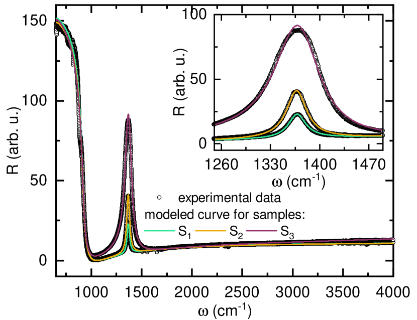
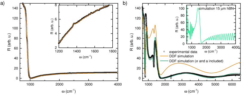
In FIG. 1 we present an exemplary spectrum modelling for three different samples. The samples were grown using three different growth conditions that resulted in different material properties (i.e. strain, amount of defects, thickness). The modelling works well for each of the samples. The values of the modelled parameters are presented in TAB. 1. The peak position at about 1367 cm-1 corresponds to the phonon mode of sp2 hybridized boron nitride [26]. The high quality is manifested by the values of the parameter for the mode, which are relatively small compared to the values reported for epitaxial layers [18, 27, 28, 29]. The inset in FIG. 1 shows that the peak intensity directly depends on the thickness of hBN. The high reflectivity below 1000 cm-1 is connected to the presence of sapphire substrate [30]. One can see that the modeled curves in FIG. 1 describe experimental data almost entirely. All important features of the spectrum are reproduced and the values in TAB. 1 are very precisely determined with relative error values for and for and . This precision enables to detect smallest deviations in strain, quality and thickness of epitaxial layers. Furthermore, due to modeling parameters related to sapphire (, ), one can monitor the quality of the substrate on which hBN was grown or deposited.
The principal advantage of the described method over the very basic peak Lorentzian fitting is the access to the physical properties of the sample, even if the sample structure is complex. The absorption shape modified by the damping parameter which influences the peak position or layer thickness is out of range for simple fitting. The thickness results coming from our method are in very good agreement with the results obtained with XRR for the samples in the range 2-70 nm (see Supplementary Materials FIG. S1). The method can be applied for samples in the thickness range from a single atomic layer to several m (see Supplementary Materials FIG. S2).
III RESULTS AND DISCUSSION
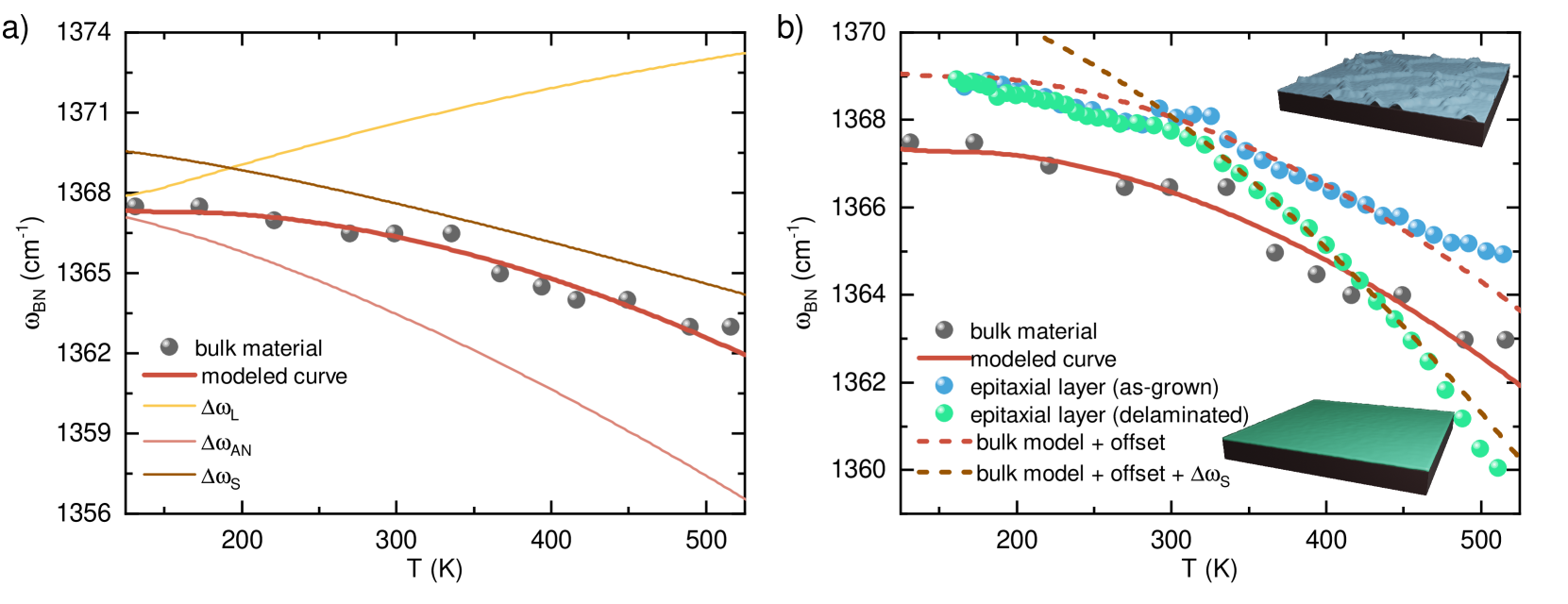
Since the phonon energy is a good indicator for strain [28], we investigated as-grown and delaminated samples. Due to the delamination process, both samples should exhibit different layer-substrate interactions. The interactions change with temperature because of the difference in the thermal expansion coefficients of the layer and the substrate. As we provided a reliable method for the identification of the phonon energy of hBN, it is possible to analyze the temperature dependencies of the lattice vibrations of the epitaxial layers . As we present in FIG. 2, the phonon energy for as-grown and delaminated layers follows different trends. To be able to extract information about layer-substrate interactions, we need to know what influences this dependency. It is governed by 4 dominant factors: the undisturbed phonon energy at 0 K , the lattice constant change (thermal expansion) , the anharmonic phonon decay , the layer-substrate interaction caused by the difference in thermal expansion coefficients of layer and substrate:
| (1) |
Taking the hBN thermal expansion coefficient provided by Yates et al. [16], and using it for the Density Functional Theory (DFT) calculations as presented by Cusco et al. [32], one can obtain the energy change due to the thermal expansion coefficient:
| (2) |
According to DFT calculations, the phonon has two dominant decay paths: three-phonon process and four-phonon process [31]. Both give the following contribution to [33]:
| (3) | |||||
where - constants are related to three- and four-phonon processes respectively, ( - Planck constant, - speed of light, - Boltzman constant, - phonon energy). In Eq. 3 we assumed that in both three- and four-phonon processes, there is the same energy decay product. This assumption is justified since in both decays the produced lower energy phonons are along the - line in the dispersion relation, which is flat. The change related to the layer interaction with the substrate can be described with the following formula:
| (4) |
where is the thermal expansion coefficient for sapphire and BN, is the hBN Grüneisen parameter and is the temperature at which the layer on the substrate is relaxed. For the as-grown layer, it is the growth temperature, and for the delaminated layer it is room temperature. All the described contributions of dependency are plotted in FIG. 2a.
Using the model that does not include the layer-substrate interaction, we can fit the line that follows experimental data for bulk material reported by Segura et al. [31]. This gives the following values of parameters: cm-1, cm-1, cm-1 and K. It corresponds to the decay to two phonons of energies 257 cm-1 and 1119 cm-1 in the three-phonon process, two phonons of energy 257 cm-1 and one phonon of energy 862 cm-1 in four-phonon process. These results are in good agreement with the literature values [26, 32].
In FIG. 2b we present the dependence of for the epitaxial layers. Both sets of results were collected for samples grown in the same MOVPE process. However, one of them was delaminated and transferred to a new sapphire substrate. The method used for delamination and transfer is as described in the literature [22]. The blue spheres related to the as-grown sample follow the same trend as the data for bulk material, which illustrates a dark red dashed line. The line is drawn by adding a constant offset to the modeled curve for bulk hBN. The shift towards higher energies is due to a higher amount of defects in the epitaxial layer, which leads to additional strain. This additional effect does not allow for reliable parameters modeling because of an unknown temperature-dependent behaviour of defects. It is suggested that the defect contribution should be linear [28]. Adding a further linear or quadratic term to the model would strongly influence other parameters which at this point are in good agreement with the literature values. We later show that defects indeed play an important role and that the assumption of a linear defect contribution is not always justified. For this reason, we provide only qualitative results.
The green spheres related to the delaminated sample exhibit a more significant decrease in phonon energy with increasing temperature. This decrease is most likely caused by a stronger layer-substrate interaction, as suggested by the brown dashed line which was created by adding term to the dark red dashed line. To cover the experimental data in a as wide as possible range, we assumed the hBN Grüneisen parameter cm-1/%. This value is over two times lower than reported for hBN before [34]. The main reason for the change of layer-substrate interaction before and after delamination is the presence and lack of characteristic wrinkles. They are created during the cooling of the material after the growth process and can be removed in the delamination process [22]. The results presented in FIG. 2b imply that in the as-grown layer, the wrinkles can compensate for the layer-substrate strain. Consequently, the blue spheres run parallel to the modeled curve for the bulk material, as the dark red dashed line suggests. The strain in the case of the as-grown epitaxial layer is eliminated by excess material stored in the wrinkles. The same behaviour is observed for the delaminated layer below room temperature at which the delamination process occurred. When cooling the relaxed delaminated layer, the wrinkles can be created and compensate for the layer-substrate strain. Consequently, the trend below room temperature is similar for both delaminated and as-grown layers. Equally, the effect of the decrease in phonon energy related to contribution for as-grown layers could be observed at much higher temperatures, which are closer to the growth temperature at which the wrinkles should disappear.

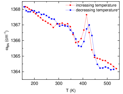
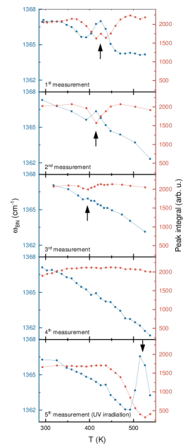
The most striking result that emerges from our measurements is a giant, anomalous shift of the phonon energy which we observed for some samples. In FIG. 3 we present the dependence for a 20 nm thick layer grown in the Two-stage Epitaxy regime. One can notice an anomalous increase of phonon energy at 425 K for the 1st measurement. This increase cannot be explained by the presented model. When performing consecutive temperature-dependent measurements, the anomaly softens and its maximum slightly moves towards lower temperatures as presented for 2nd and 3rd measurement. In the 4th temperature run, no anomalous phonon behaviour is observed. To make sure that the effect is not an artifact of our data analysis method, we performed basic peak Lorentzian fitting on the measured data set. In this approach, the anomaly is still observed at the same temperatures (see Supplementary Materials).
We also observed the described anomalous behavior of dependence for other samples grown under different regimes under NH3-rich conditions before and after the delamination process (see Supplementary Materials). The anomaly occurrence for different samples implies that the phonon upshift is not an accidental effect related to one specific sample, but can be reproduced when a special set of growth parameters is applied. The observation of the effect occurrence for both as-grown and delaminated layers proves that it does not come from the substrate or thin AlN layer on Al2O3-hBN interface but it is attributed to the hBN layer itself.
In the following measurements presented in FIG. 3, there is a more steep decrease in energy with increasing temperature. The same effect is observed when we compare the results for as-grown and delaminated layers in FIG. 2b. In this case, it is most likely related to changes in the layer wrinkle pattern. As the result suggests, the wrinkle pattern can be changed for temperatures much lower than the growth temperature. Wrinkles rearrangement leads to an increase in the layer-substrate interaction contribution what is observed in the energy downshift for higher temperatures, as suggested by the brown curve in FIG. 2a.
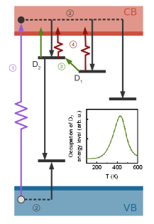
Once the anomaly vanishes after consecutive temperature runs, we can restore it by UV irradiation. The anomaly measured after UV irradiation in the 5th run is much stronger and appears at higher temperature as presented in FIG. 3. The increase in phonon energy is cm-1. We propose the mechanism presented in FIG. 4 to explain the observed phenomenon. When the sample is exposed to UV light, electrons from the valence band are transferred to the conduction band (CB) (\raisebox{-0.9pt}{1}⃝). Then they can be trapped on a shallow defect just below the conduction band (\raisebox{-0.9pt}{2}⃝). Here, we assume that defect energy level is less than 1 eV below the conduction band, which has high degeneracy. The state can be filled during the growth process as well. These kinds of traps can store carriers for a significant time [35]. If the material has an additional defect state in between state and the CB, we can change the occupation probability of all three states during the measurement by changing the temperature (\raisebox{-0.9pt}{3}⃝). For a specific temperature, the occupation of the defect state reaches the maximum value. The change in electrical state of leads to the expansion of the defect. Consequently, an inhomogeneous compressive strain is introduced. For such conditions, the phonon energy increases. This dependence between the electric state of the defect and the phonon energy suggests the presence of a strong electron-phonon coupling in those epitaxial hBN, in particular as comparing to the bulk material [35]. A further temperature increase transfers electrons to the conduction band. Because the traps are situated close to the conduction band, they can be refilled with electrons. Then the anomalous effect is repeated for the next temperature-dependent measurement until we empty most of the shallow traps, and electrons occupy deeper donor levels. Further evidence for the presented mechanism is provided by the fact that the anomaly is observed in both directions, for an increase as well as for a consecutive decrease in temperature (see Supplementary Materials). We do not exclude that the presented mechanism could be occurring symmetrically for the valence band and acceptor states.
The defects properties in hBN are complicated and not fully understood. For this reason, it is hard to pinpoint defects and . However, we have candidates that meet the described criteria. It has been reported that the energy levels of are shallow traps placed below the conduction band in hBN [36, 37, 38, 39, 40]. At very high temperature during the growth process, oxygen atoms diffuse and desorp from the Al2O3 substrate [41]. Consequently, the substrate can be a source of oxygen atoms in the hBN layer that replace nitrogen atoms. Such a defect has a low formation energy [36], so it should be present in all high-temperature grown epitaxial layers. The defect is therefore a good candidate for the defect.
The studied hBN layer was grown in the Two-stage Epitaxy regime in NH3 rich conditions [20] which supports the creation of [36]. in 1- and 2- charge states increases the distortion between nitrogen atoms [36] which leads to lattice compressive strain in vicinity of the defect. Moreover, has an energy similar to that of the defect and the complex [36]. Therefore, we speculate that the defect can be a negatively charged boron vacancy.
The anomaly presented in FIG. 3 occurs in a narrower range of temperatures in comparison to the simulation in the inset in FIG. 4. That suggests that there are other effects that enhance the anomalous phonon energy behaviour. Such an effect could be the piezoelectric response of boron nitride which is observed for different phases of sp2-BN [42, 43, 44]. Such non-centrosymetric phases, which exhibit piezoelectricity, are present in epitaxial boron nitride layers [21]. Moreover, there is evidence of a strong electrostrictive effect in boron nitride nanotubes [45, 46]. Electrostriction depends quadratically on the electric field. Therefore, the reverse of the field does not reverse the direction of strain. Consequently, the strain does not disappear when considering diferent randomly arranged BN grains. The deformation related to the electrostrictive effect is much greater compared to traditional piezoceramics [46]. Consequently, the electric field induced by charge redistribution on defect states would significantly influence the phonon energy change as observed in the experiment.
IV CONCLUSIONS
In this work, we studied the thermal response of the phonon mode in boron nitride epitaxial layers using Fourier-transform infrared spectroscopy. The developed FTIR spectra analysis provided reliable information about the physical properties of epitaxial layers which are in good agreement with the X-ray reflectometry results. Both methods are complementary. However, our method allows to analyze a wide range of samples, from a single atomic monolayer to a few tens of m. The upper thickness limit depends on the quality of the sample. We can also obtain information about surface roughness or material porosity. The method can be easily extended to other materials and structures.
In our study, we investigated as-grown as well as delaminated layers. The results of temperature-dependent measurements emphasize the importance of layer wrinkles in the layer-substrate interaction. The wrinkles significantly reduce the strain on the interface. Consequently, the behaviour of the epitaxial layer is similar to that of the bulk material.
Furthermore, we observed strong electron-phonon coupling, which can lead to a phonon energy increase up to 6 cm-1. This anomalous behaviour vanishes after sample heating and cooling cycles. Importantly, the process can be enhanced by UV irradiation. This effect can be explained by the presence of defects (, ) close to the conduction band. The exact nature of such defects is still unknown. However, we speculate that these defects could be and or their complexes. By increasing the occupation of the upper energy state, we introduce an inhomogeneous compressive strain which leads to an anomalous increase in phonon energy. Most likely, the observed anomaly is enhanced by other effects such as piezoelectricity and electrostriction. However, more research is needed to investigate the exact properties of shallow impurity states and their influence on the properties of hBN.
Acknowledgements.
This work was supported by the National Science Centre, Poland, under the decisions 2019/33/B/ST5/02766 and 2020/39/D/ST7/02811.References
- Zunger et al. [1976] A. Zunger, A. Katzir, and A. Halperin, Optical properties of hexagonal boron nitride, Physical Review B 13, 5560 (1976).
- Ohba et al. [2001] N. Ohba, K. Miwa, N. Nagasako, and A. Fukumoto, First-principles study on structural, dielectric, and dynamical properties for three BN polytypes, Physical Review B 63, 10.1103/physrevb.63.115207 (2001).
- Viana et al. [2020] G. E. D. Viana, A. M. Silva, F. U. da C. Barros, F. J. A. M. da Silva, E. W. S. Caetano, J. J. S. Melo, and A. Macedo-Filho, Thermal stability and electronic properties of boron nitride nanoflakes, Journal of Molecular Modeling 26, 10.1007/s00894-020-4321-z (2020).
- Chen et al. [2004] Y. Chen, J. Zou, S. J. Campbell, and G. L. Caer, Boron nitride nanotubes: Pronounced resistance to oxidation, Applied Physics Letters 84, 2430 (2004).
- Kostoglou et al. [2015] N. Kostoglou, K. Polychronopoulou, and C. Rebholz, Thermal and chemical stability of hexagonal boron nitride (h-BN) nanoplatelets, Vacuum 112, 42 (2015).
- Sevik et al. [2011] C. Sevik, A. Kinaci, J. B. Haskins, and T. Çağın, Characterization of thermal transport in low-dimensional boron nitride nanostructures, Physical Review B 84, 10.1103/physrevb.84.085409 (2011).
- Jadczak et al. [2021] J. Jadczak, J. Kutrowska-Girzycka, J. J. Schindler, J. Debus, K. Watanabe, T. Taniguchi, C.-H. Ho, and L. Bryja, Investigations of electron-electron and interlayer electron-phonon coupling in van der waals hBN/WSe2/hBN heterostructures by photoluminescence excitation experiments, Materials 14, 399 (2021).
- Prazdnichnykh et al. [2021] A. I. Prazdnichnykh, M. M. Glazov, L. Ren, C. Robert, B. Urbaszek, and X. Marie, Control of the exciton valley dynamics in atomically thin semiconductors by tailoring the environment, Physical Review B 103, 10.1103/physrevb.103.085302 (2021).
- Li et al. [2017] C. Li, P. Zhou, and D. W. Zhang, Devices and applications of van der waals heterostructures, Journal of Semiconductors 38, 031005 (2017).
- Binder et al. [2017] J. Binder, F. Withers, M. R. Molas, C. Faugeras, K. Nogajewski, K. Watanabe, T. Taniguchi, A. Kozikov, A. K. Geim, K. S. Novoselov, and M. Potemski, Sub-bandgap voltage electroluminescence and magneto-oscillations in a WSe2 light-emitting van der waals heterostructure, Nano Letters 17, 1425 (2017).
- Seitz et al. [2019] M. Seitz, P. Gant, A. Castellanos-Gomez, and F. Prins, Long-term stabilization of two-dimensional perovskites by encapsulation with hexagonal boron nitride, Nanomaterials 9, 1120 (2019).
- Lee et al. [2015] G.-H. Lee, X. Cui, Y. D. Kim, G. Arefe, X. Zhang, C.-H. Lee, F. Ye, K. Watanabe, T. Taniguchi, P. Kim, and J. Hone, Highly stable, dual-gated MoS2 transistors encapsulated by hexagonal boron nitride with gate-controllable contact, resistance, and threshold voltage, ACS Nano 9, 7019 (2015).
- Ahn et al. [2016] S. Ahn, G. Kim, P. K. Nayak, S. I. Yoon, H. Lim, H.-J. Shin, and H. S. Shin, Prevention of transition metal dichalcogenide photodegradation by encapsulation with h-BN layers, ACS Nano 10, 8973 (2016).
- Ludwiczak et al. [2021] K. Ludwiczak, A. K. Dąbrowska, J. Binder, M. Tokarczyk, J. Iwański, B. Kurowska, J. Turczyński, G. Kowalski, R. Bożek, R. Stępniewski, W. Pacuski, and A. Wysmołek, Heteroepitaxial growth of high optical quality, wafer-scale van der waals heterostrucutres, ACS Applied Materials & Interfaces 13, 47904 (2021).
- Pacuski et al. [2020] W. Pacuski, M. Grzeszczyk, K. Nogajewski, A. Bogucki, K. Oreszczuk, J. Kucharek, K. E. Połczyńska, B. Seredyński, A. Rodek, R. Bożek, T. Taniguchi, K. Watanabe, S. Kret, J. Sadowski, T. Kazimierczuk, M. Potemski, and P. Kossacki, Narrow excitonic lines and large-scale homogeneity of transition-metal dichalcogenide monolayers grown by molecular beam epitaxy on hexagonal boron nitride, Nano Letters 20, 3058 (2020).
- Yates et al. [1975] B. Yates, M. J. Overy, and O. Pirgon, The anisotropic thermal expansion of boron nitride, Philosophical Magazine 32, 847 (1975).
- Pakuła et al. [2019] K. Pakuła, A. Dąbrowska, M. Tokarczyk, R. Bożek, J. Binder, G. Kowalski, A. Wysmołek, and R. Stępniewski, Fundamental mechanisms of hbn growth by movpe (2019), arXiv:1906.05319 .
- Chugh et al. [2018] D. Chugh, J. Wong-Leung, L. Li, M. Lysevych, H. H. Tan, and C. Jagadish, Flow modulation epitaxy of hexagonal boron nitride, 2D Materials 5, 045018 (2018).
- Kobayashi et al. [2008] Y. Kobayashi, T. Akasaka, and T. Makimoto, Hexagonal boron nitride grown by movpe, Journal of Crystal Growth 310, 5048 (2008).
- Dąbrowska et al. [2020] A. K. Dąbrowska, M. Tokarczyk, G. Kowalski, J. Binder, R. Bożek, J. Borysiuk, R. Stępniewski, and A. Wysmołek, Two stage epitaxial growth of wafer-size multilayer h-BN by metal-organic vapor phase epitaxy – a homoepitaxial approach, 2D Materials 8, 015017 (2020).
- Moret et al. [2021] M. Moret, A. Rousseau, P. Valvin, S. Sharma, L. Souqui, H. Pedersen, H. Högberg, G. Cassabois, J. Li, J. H. Edgar, and B. Gil, Rhombohedral and turbostratic boron nitride: X-ray diffraction and photoluminescence signatures, Applied Physics Letters 119, 262102 (2021).
- Iwański et al. [2021] J. Iwański, A. Dąbrowska, M. Tokarczyk, J. Binder, R. Stępniewski, and A. Wysmołek, Delamination of large area layers of hexagonal boron nitride grown by MOVPE, Acta Physica Polonica A 139, 457 (2021).
- Parratt [1954] L. G. Parratt, Surface studies of solids by total reflection of x-rays, Physical Review 95, 359 (1954).
- Fewster [2003] P. Fewster, X-ray scattering from semiconductors (Imperial College Press, London, 2003) p. 83.
- Fewster [1996] P. F. Fewster, X-ray analysis of thin films and multilayers, Reports on Progress in Physics 59, 1339 (1996).
- Geick et al. [1966] R. Geick, C. H. Perry, and G. Rupprecht, Normal modes in hexagonal boron nitride, Physical Review 146, 543 (1966).
- Caban et al. [2020] P. Caban, P. Michalowski, I. Wlasny, J. Gaca, M. Wojcik, P. Ciepielewski, D. Teklinska, and J. Baranowski, Carbon incorporation in boron nitride grown by MOCVD under n2 flow, Journal of Alloys and Compounds 815, 152364 (2020).
- Bera et al. [2020] K. Bera, A. Roy, D. Chugh, J. Wong-Leung, H. H. Tan, and C. Jagadish, Role of defects and grain boundaries in the thermal response of wafer-scale hBN films, Nanotechnology 32, 075702 (2020).
- Wang et al. [2021] G. Wang, J. Chen, J. Meng, Z. Yin, J. Jiang, Y. Tian, J. Li, J. Wu, P. Jin, and X. Zhang, Direct growth of hexagonal boron nitride films on dielectric sapphire substrates by pulsed laser deposition for optoelectronic applications, Fundamental Research 1, 677 (2021).
- Lee et al. [2014] S. Lee, S. Ng, H. A. Hassan, Z. Hassan, and T. Dumelow, Crystal orientation dependence of polarized infrared reflectance response of hexagonal sapphire crystal, Optical Materials 37, 773 (2014).
- Segura et al. [2020] A. Segura, R. Cuscó, T. Taniguchi, K. Watanabe, and L. Artús, Long lifetime of the e1u in-plane infrared-active modes of h -BN, Physical Review B 101, 10.1103/physrevb.101.235203 (2020).
- Cuscó et al. [2016] R. Cuscó, B. Gil, G. Cassabois, and L. Artús, Temperature dependence of raman-active phonons and anharmonic interactions in layered hexagonal BN, Physical Review B 94, 10.1103/physrevb.94.155435 (2016).
- Balkanski et al. [1983] M. Balkanski, R. F. Wallis, and E. Haro, Anharmonic effects in light scattering due to optical phonons in silicon, Physical Review B 28, 1928 (1983).
- Androulidakis et al. [2018] C. Androulidakis, E. N. Koukaras, M. Poss, K. Papagelis, C. Galiotis, and S. Tawfick, Strained hexagonal boron nitride: Phonon shift and grüneisen parameter, Physical Review B 97, 10.1103/physrevb.97.241414 (2018).
- Wlasny et al. [2019] I. Wlasny, K. Pakula, R. Stepniewski, W. Strupinski, I. Pasternak, J. M. Baranowski, and A. Wysmolek, Sts observations of deep defects within laser-illuminated graphene/movpe-h-bn heterostructures, Applied Physics Letters 114, 102103 (2019), https://doi.org/10.1063/1.5081487 .
- Weston et al. [2018] L. Weston, D. Wickramaratne, M. Mackoit, A. Alkauskas, and C. G. V. de Walle, Native point defects and impurities in hexagonal boron nitride, Physical Review B 97, 10.1103/physrevb.97.214104 (2018).
- Katzir et al. [1975] A. Katzir, J. T. Suss, A. Zunger, and A. Halperin, Point defects in hexagonal boron nitride. i. EPR, thermoluminescence, and thermally-stimulated-current measurements, Physical Review B 11, 2370 (1975).
- Vokhmintsev et al. [2017] A. Vokhmintsev, M. Minin, and I. Weinstein, Estimation of thermoluminescence kinetic parameters in h-BN by different techniques, Radiation Measurements 106, 55 (2017).
- Vokhmintsev et al. [2019] A. Vokhmintsev, I. Weinstein, and D. Zamyatin, Electron-phonon interactions in subband excited photoluminescence of hexagonal boron nitride, Journal of Luminescence 208, 363 (2019).
- Vokhmintsev and Weinstein [2021] A. Vokhmintsev and I. Weinstein, Temperature effects in 3.9 eV photoluminescence of hexagonal boron nitride under band-to-band and subband excitation within 7–1100–k range, Journal of Luminescence 230, 117623 (2021).
- Matsuoka and Kangawa [2018] T. Matsuoka and Y. Kangawa, eds., Epitaxial Growth of III-Nitride Compounds (Springer International Publishing, 2018) pp. 199–214.
- Kundalwal et al. [2021] S. Kundalwal, V. Choyal, V. Choyal, S. Nevhal, and N. Luhadiya, Enhancement of piezoelectric and flexoelectric response of boron nitride sheet superlattices via interface and defect engineering, Physica E: Low-dimensional Systems and Nanostructures 127, 114563 (2021).
- Michel and Verberck [2011] K. H. Michel and B. Verberck, Phonon dispersions and piezoelectricity in bulk and multilayers of hexagonal boron nitride, Physical Review B 83, 10.1103/physrevb.83.115328 (2011).
- Brazhe and Dolgov [2020] R. A. Brazhe and D. A. Dolgov, Transverse piezo- and pyroelectric effects in 2d nanoallotropes of boron nitride caused by the ripple formation, Physics of the Solid State 62, 1421 (2020).
- Kang et al. [2015] J. H. Kang, G. Sauti, C. Park, V. I. Yamakov, K. E. Wise, S. E. Lowther, C. C. Fay, S. A. Thibeault, and R. G. Bryant, Multifunctional electroactive nanocomposites based on piezoelectric boron nitride nanotubes, ACS Nano 9, 11942 (2015).
- Dai et al. [2009] Y. Dai, W. Guo, Z. Zhang, B. Zhou, and C. Tang, Electric-field-induced deformation in boron nitride nanotubes, Journal of Physics D: Applied Physics 42, 085403 (2009).
- Malitson [1962] I. H. Malitson, Refraction and dispersion of synthetic sapphire, Journal of the Optical Society of America 52, 1377 (1962).
- Knittl [1976] Z. Knittl, Optics of thin films; an optical multilayer theory (Wiley, London,New York, 1976) pp. 46–51.
- Chubarov et al. [2018] M. Chubarov, H. Högberg, A. Henry, and H. Pedersen, Review article: Challenge in determining the crystal structure of epitaxial 0001 oriented sp2-BN films, Journal of Vacuum Science & Technology A: Vacuum, Surfaces, and Films 36, 030801 (2018).
Supplementary materials
FTIR spectra analysis method
To simulate the whole FTIR spectrum, we assume that the medium is composed of harmonic damped oscillators. Then Dynamic Dielectric Function (DDF) for hBN is given by [26]:
| (5) |
where , cm-2, cm-2, and are the frequencies of the normal modes and respectively and are the corresponding damping parameters. For sapphire dielectric function is described as follows [30]:
| (6) |
where and are the frequencies of longitudinal and transverse optic normal modes in sapphire, and are their damping parameters. is given by the formula [47]:
| (7) |
The values of the parameters connected to sapphire are taken from the papers by Lee et al. [30] and Malitson [47]. In the next step, we assume that incident light is reflected from air-hBN and hBN-Al2O3 interfaces and the light transmitted into the sapphire is fully absorbed and does not interact with the beam reflected on the interfaces. The light beams reflected from the following interfaces interfere with each other. That leads to the formula for the reflection coefficient for the structure of a thin layer grown on the sapphire substrate [48].
| (8) | |||
| (9) |
where is the optical path difference for light that penetrates the hBN layer, - thickness of the hBN layer and , are complex refractive indices of hBN and sapphire described by the square root of their dielectric functions (). Finally, by calculating the square of the absolute value of the reflection coefficient, it is possible to simulate the reflectivity curve of the analyzed structure (, where is a normalization factor).
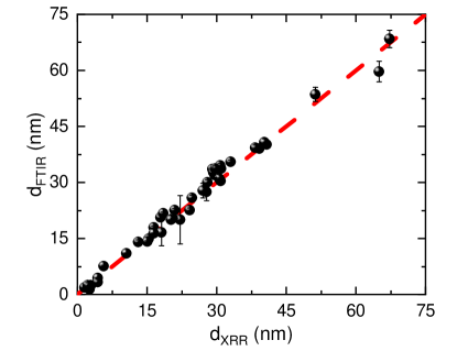
To verify the propriety of the results coming from the described FTIR spectra analysis method, we compared them with the results obtained with an independent measurement technique, which is X-ray reflectometry. The values of hBN thickness for the samples in range nm obtained from FTIR () and XRR () measurements are plotted in FIG. S1. The values presented are the average of values coming from the 3 measured areas. The error bars are their standard deviation. The uncertainty of the fitted values is about 1 nm. The points lie on the dashed line described by the formula . This indicates a very good agreement between both methods over a wide range of sample thickness.
The next step in the introduction of the method is to define its limitations. In FIG. S2a we present the spectrum for the thinnest measured sample. The peak related to the mode in hBN is barely visible. Implementation of our method revealed nm. This value is slightly lower than the thickness of the hBN monolayer [49]. This is because the measured area of m is not fully covered by the hBN layer. However, the data presented in FIG. S2a proves that our method has no lower limitations in the context of sp2-BN detection and enables atomic monolayer characterization.
The spectrum for the thickest measured layer is presented in FIG. S2b. For this sample, we measured spectra in the range up to 6500 cm-1 for better observation of characteristic oscillations related to interference within the hBN layer. Due to the roughness and porosity of thick epitaxial layers, we cannot use our model to describe the experimental data. However, we can introduce some amendments to the model. To take into account the roughness , we change the expression for the reflection coefficient as follows:
| (10) |
To consider the porosity of the material, we use a simple model in which we decrease the dielectric function with the parameter .
| (11) |
When Eq. 10-11 are introduced it is possible to model a curve which describes the experimental data much better as presented in FIG. S2b. The fitting procedure revealed the thickness of the hBN layer nm, surface roughness nm, porosity . The simulation presented in FIG. S2b inset suggests that using our method it would be possible to analyze crystals that are tens of micrometers thick. All this shows high universality of our method, which allows analyzing layers in the range from single atomic layers up to several m.
Simulation of temperature dependence of defect occupation
We assume a three-level energy model (). The highest energy level is the conduction band, which is represented by its high degeneracy . The middle energy level can be degenerated as well (). Occupation is governed by the Boltzmann distribution. We allow only thermal electron excitation. Then the occupation for the following energy levels will be given by:
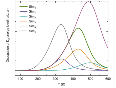
where -temperature, -Boltzmann constant, -energy distance between states and . For the case of analyzed defects in hBN: eV, [36, 39]. FIG. S3 presents the results of simulations with different sets of modeled parameters. The values of the parameters for each simulation are presented in TAB. S1. One can observe the simulated peak movement and its intensity change while changing parameters. The curve and parameters related to Sim0 correspond to the simulation presented in the main text in FIG. 4.
| Simulation | (eV) | (eV) | ||
|---|---|---|---|---|
| Sim0 | 0.158 | 0.573 | 2 | |
| Sim1 | 0.158 | 0.400 | 2 | |
| Sim2 | 0.250 | 0.573 | 2 | |
| Sim3 | 0.158 | 0.573 | 1 | |
| Sim4 | 0.158 | 0.573 | 2 | |
| Sim5 | 0.100 | 0.400 | 1 |
Anomaly observed for different samples

| Sample | Growth mode | (∘C) | NH3 flow (ccm) | TEB flow (ccm) | (nm) |
|---|---|---|---|---|---|
| FME | 1295 | 4000 | 15 | 10.7 | |
| CFG | 1315 | 4000 | 10 | 5.2 | |
| Two-stage | 1309/1300 | 4000 | 10/15 | 15.4 | |
| Two-stage | 1305/1300 | 4000 | 10/15 | 36.8 | |
| Two-stage | 1295/1285 | 4000 | 10/15 | 8.5 | |
| Two-stage | 1295/1285 | 4000 | 10/15 | 8.0 |