SSurvey Sources
IEEEexample:BSTcontrol \bstctlcite[@auxoutS]IEEEexample:BSTcontrol \setbiblabelwidth1000
IEEEexample:BSTcontrol
DISS. ETH NO. 27894
ENABLING EFFECTIVE ERROR MITIGATION
IN MEMORY CHIPS
THAT USE ON-DIE ERROR-CORRECTING CODES
A thesis submitted to attain the degree of
DOCTOR OF SCIENCES of ETH ZÜRICH
(Dr. sc. ETH Zürich)
presented by
MINESH PATEL
born on 22 October 1992
citizen of the United States of America
accepted on the recommendation of
Prof. Dr. Onur Mutlu, examiner
Prof. Dr. Mattan Erez, co-examiner
Prof. Dr. Moinuddin Qureshi, co-examiner
Dr. Vilas Sridharan, co-examiner
Dr. Christian Weis, co-examiner
2021
Minesh Patel: Enabling Effective Error Mitigation in Memory Chips That Use On-Die Error-Correcting Codes, © 2021
To my loving parents, Alpa and Hamen, and my sister, Shreya.
Acknowledgments
This thesis is the culmination of six years of effort throughout my graduate studies, and a vast number of individuals contributed either directly or indirectly. These acknowledgments comprise my reflections on their influence herein.
First and foremost, I thank my adviser, Onur Mutlu, for shaping me into the individual I am today. Through his supervision, the environment he has built in SAFARI, and the trust he has put in me, I have acquired the expertise, tools, and mindset I need to better understand myself, my goals, and my work. Although I cannot know how or where I will apply these skills in the future, I am certain that they will be central to my continued development as a researcher, scientist, and engineer.
I thank my committee members, Mattan Erez, Moinuddin Qureshi, Vilas Sridharan, and Christian Weis, for supervising this thesis. Your feedback is integral to improving both the thesis and its constituent works, and I look forward to seeing the impact this work has due to our collective efforts.
I thank the many anonymous peer reviewers who vetted my work across many conference submissions to ISCA, MICRO, HPCA, ASPLOS, and DSN. They provided the external expert feedback necessary to identify and address the weaknesses of the works, allowing us to improve their scientific value and resulting impact.
I am grateful for the SAFARI group members who helped and supported me along the way, both in a working and social capacity. At its foundation, the Ph.D. has been a lonely journey. However, you all minimized the impact of that isolation, turning an otherwise independent process into something much, much more. In particular, I thank Jeremie Kim for his time and energy as a friend, sounding board, confidant, roommate, and generally someone who was always willing to listen. I thank Amirali Boroumand and Saugata Ghose, who helped guide me through my first days in the Ph.D. with their friendship and support. I thank the others I interacted with during my time at CMU, including Nandita Vijaykumar, Vivek Seshadri, Samira Khan, Rachata Ausavarungnirun, Hongyi Xin, Yang Li, Kevin Chang, Kevin Hsieh, Yixin Luo, and Donghyuk Lee for their advice and support during my early years. Similarly, I thank those I got to know at ETH, including Hasan Hassan, Giray Yağlıkçı, Geraldo Franciso de Oliveira, Taha Shahroodi, Nastaran Hajinazar, Roknoddin Azizi, Can Fırtına, Nika Mansouri-Ghiasi, Konstantinos Kanellopoulos, Rahul Bera, Jisung Park, Arash Tavakkol, Lois Orosa, Juan Gomez-Luna, and many others for their support, both in the context of friendship and research. I would also like to extend a special thank you to Max Rumpf and Arvid Gollwitzer for helping me with translating my abstract into German.
Durign my time at CMU and ETH, I met many wonderful people who helped me adjust and enjoy my time outside of lab. At CMU, I thank my roommate, Dipanjan Saha, whose friendship was essential to surviving my sojourn into the winter wonderland that is Pittsburgh; Vignesh Balaji, with whom I shared the experience of the Ph.D. life like no other; and Madhav Iyengar, who supported me with his constant friendship. At ETH, I thank my roommate, Dominik Christe, and the Systems Group members, including Johannes de Fine Licht, Kaan Kara, David Sidler, and Ghislain Fourny, who helped me adjust to life in Zürich and ETH.
I thank my internship mentors, including Tyler Huberty, Stephan Meier, Jared Zerbe, Heonjae Ha, Seung Lee, Griffin Branham, Taehyun Kim from Apple and Stefan Saroiu and Alec Wolman from Microsoft Research for guiding me in both my work at the company and my research in general. I am glad to have worked with them and have my perspectives broadened.
I am eternally grateful for my family and friends from back home, whose uncompromising support and encouragement was essential for me to make it this far in my own journey. I thank Philip Li, Thejas Prasad, Rohan Mutalik, Chirag Sakhuja, Nikhil Joglekar, Karthik Sethuraman, Alex Hsu, Kevin Pham, Kevin Chen, Nikhil Dixit, Chris Roberts, Sean Shen, Nathan Kwan, Sudha Verma, and the many others who helped me through the more difficult times. In many ways, I believe that these individuals took the same journey with me, side-by-side, in spirit.
I thank all the industrial partners who provided funding to support this work: Microsoft, Intel, Google, IBM, Facebook, Qualcomm, VMware, NVIDIA, Samsung, Alibaba, Huawei.
Finally, my most important thank you goes to my parents, Alpa and Hamen Patel, and my sister, Shreya Patel, for their love, support, and encouragement throughout my journey to advance the state-of-the-art. Scientific contribution is difficult, and its success is grounded on the foundation you provided me with through your own efforts and dedication. I am endlessly grateful for the opportunities I have had, and I thank you all, in addition to my cousins, aunts, uncles, and other family members who stood by me, for making this possible.
Abstract
Improvements in main memory storage density are primarily driven by process technology shrinkage (i.e., technology scaling), which negatively impacts reliability by exacerbating various circuit-level error mechanisms. To compensate for growing error rates, both memory manufacturers and consumers develop and incorporate error-mitigation mechanisms that improve manufacturing yield and allow system designers to meet reliability targets. Developing effective error mitigation techniques requires understanding the errors’ characteristics (e.g., worst-case behavior, statistical properties). Unfortunately, we observe that proprietary on-die Error-Correcting Codes (ECC) used in modern memory chips introduce new challenges to efficient error mitigation by obfuscating CPU-visible error characteristics in an unpredictable, ECC-dependent manner.
In this dissertation, we experimentally study memory errors, examine how on-die ECC obfuscates their statistical characteristics, and develop new testing techniques to overcome the obfuscation through four key steps. First, we experimentally study DRAM data-retention error characteristics to understand the challenges inherent in understanding and mitigating memory errors that are related to technology scaling. Second, we study how on-die ECC affects these characteristics to develop Error Inference (EIN), a new statistical inference methodology for inferring key details of the on-die ECC mechanism and the raw errors that it obfuscates. Third, we examine the on-die ECC mechanism in detail to understand exactly how on-die ECC obfuscates raw bit error patterns. Using this knowledge, we introduce Bit Exact ECC Recovery (BEER), a new testing methodology that exploits uncorrectable error patterns to (1) reverse-engineer the exact on-die ECC implementation used in a given memory chip and (2) identify the bit-exact locations of the raw bit errors responsible for a set of errors that are observed after on-die ECC correction. Fourth, we study how on-die ECC impacts error profiling and show that on-die ECC introduces three key challenges that negatively impact profiling practicality and effectiveness. To overcome these challenges, we introduce Hybrid Active-Reactive Profiling (HARP), a new error profiling strategy that uses simple modifications to the on-die ECC mechanism to quickly and effectively identify bits at risk of error. Finally, we conclude by discussing the critical need for transparency in DRAM reliability characteristics in order to enable DRAM consumers to better understand and adapt commodity DRAM chips to their system-specific needs.
This dissertation builds a detailed understanding of how on-die ECC obfuscates the statistical properties of main memory error mechanisms using a combination of real-chip experiments and statistical analyses. Our results show that the error characteristics that on-die ECC obfuscates can be recovered using new memory testing techniques that exploit the interaction between on-die ECC and the statistical characteristics of memory error mechanisms to expose physical cell behavior. We hope and believe that the analysis, techniques, and results we present in this dissertation will enable the community to better understand and tackle current and future reliability challenges as well as adapt commodity memory to new advantageous applications.
Zusammenfassung
Verbesserungen in der Arbeitsspeicherdichte werden in erster Linie durch die Miniaturisierung der Prozesstechnologie (d.h. Technologieskalierung) vorangetrieben. Diese Verkleinerung wirkt sich jedoch negativ auf die Zuverlässigkeit aus, da sie verschiedene Fehlerarten auf Schaltkreisebene verstärkt. Um diesen steigenden Fehlerraten entgegenzuwirken, entwickeln sowohl die Speicherhersteller als auch die Verbraucher Fehlerminderungstechniken, die die Fertigungsausbeute verbessern und es den Systementwicklern ermöglichen, ihre Zuverlässigkeitsziele zu erreichen. Die Entwicklung von effektiven Fehlerminderungstechniken erfordert jedoch ein genaues Verständnis der Fehlereigenschaften (z. B. Worst-Case-Verhalten, statistische Eigenschaften). Leider stellen wir fest, dass die in modernen Speicherchips eingesetzten proprietären On-Die Error-Correcting Codes (ECC) die Fehlereigenschaften auf unvorhersehbare und ECC-abhängige Weise verschleiern und somit effiziente Fehlerminderung erschweren.
In dieser Dissertation untersuchen wir Speicherfehler experimentell und betrachten, wie On-Die ECC ihre statistischen Eigenschaften verschleiert und entwickeln neue Testverfahren, um diese Verschleierung in vier Schritten zu überwinden. Um die Herausforderungen zu verstehen, die mit der Miniaturisierung zusammenhängen, untersuchen wir zunächst die DRAM-Datenerhaltungsfehlereigenschaften experimentell. Zweitens untersuchen wir, wie sich On-Die ECC auf diese Eigenschaften auswirkt und entwickeln Error Inference (EIN), eine neue statistische Inferenzmethode, mit der sich wichtige Details des On-Die ECC-Mechanismus und der von ihm verschleierten Bit-Fehler ableiten lassen. Drittens untersuchen wir den On-Die-ECC-Mechanismus, um zu verstehen, wie er Bit-Fehlermuster verschleiert. Mit diesem Wissen stellen wir Bit Exact ECC Recovery (BEER) vor, eine neue Testmethode, die unkorrigierbare Fehlermuster ausnutzt, um (1) die exakte On-Die ECC-Implementierung eines Speicherchips und (2) die genauen Stellen der Bitfehler zu bestimmen. Viertens untersuchen wir, wie On-Die ECC sich auf die Fehlerprofilierung auswirkt, und zeigen, dass On-Die ECC drei zentrale Herausforderungen birgt, die sich negativ auf die Praktikabilität und Effektivität der Profilerstellung auswirken. Zur Überwindung dieser Herausforderungen, führen wir Hybrid Active-Reactive Profiling (HARP) ein, eine neue Fehlerprofilierungsstrategie, die einfache Modifikationen am On-Die ECC-Mechanismus nutzt, um schnell und effektiv fehlergefährdete Bits zu identifizieren. Abschließend erörtern wir die kritische Notwendigkeit von Transparenz bei DRAM-Zuverlässigkeitsmerkmalen, um es DRAM-Kunden zu erlauben, handelsübliche DRAM-Chips besser zu verstehen und an ihre systemspezifischen Anforderungen anzupassen.
In dieser Dissertation wird ein detailliertes Verständnis entwickelt, wie On-Die-ECC die statistischen Eigenschaften von Arbeitsspeicherfehlern verschleiert, wozu wir Experimente auf echten Chips mit statistischen Analysen kombinieren. Unsere Ergebnisse zeigen, dass die Fehlercharakteristiken, die durch On-Die ECC verschleiert werden, mit unseren neuen Speichertesttechniken wiederhergestellt werden können. Wir hoffen und glauben, dass die Analyse, die Techniken und die Ergebnisse dieser Dissertation es Entwicklern erlauben wird, Zuverlässigkeitsprobleme besser zu verstehen und zu bewältigen sowie mit handelsüblichem Arbeitsspeicher neue, vorteilhafte Anwendungen zu erschliessen.
?chaptername? 1 Introduction
Memory has been an integral component of computing systems for over half a century [9] and has evolved alongside the rest of the system to achieve high capacity, performance, reliability, and energy-efficiency at low cost. In particular, dynamic random access memory (DRAM), first introduced by Robert Dennard at IBM in the late 1960s [9, 132, 133, 387, 439], has served as the de-facto standard main memory technology across a broad range of computing systems for decades. This is primarily due to its large, reliable storage capacity at low cost relative to other memory technologies (e.g., SRAM, Flash) [202, 395, 420, 421].
To remain competitive within the memory market while satisfying growing demands brought about by continual advancements in computing systems, DRAM manufacturers have relentlessly pursued improvements in storage density and bandwidth while minimizing the overall cost-per-bit. Manufacturers have achieved this through improving both their circuit designs and manufacturing processes (e.g., process technology scaling), enabling denser, faster memory devices [9, 276, 384, 105].
Unfortunately, these improvements exacerbate various unwanted circuit-level phenomena (e.g., charge leakage) that can lead to errors, i.e., memory cells that do not store data correctly [434, 176, 420, 369, 105]. Therefore, as manufacturers continue to improve DRAM technology, they face growing error rates that threaten both (1) DRAM manufacturers’ own device reliability and factory yield [405, 276, 461, 538, 88, 151]; and (2) system designers’ ability to build robust systems that their customers can rely upon [397, 297, 312, 435, 538].
To compensate for these errors, DRAM manufacturers incorporate error-mitigation mechanisms, which are circuits designed to prevent memory errors from causing software-visible bit flips. DRAM manufacturers choose error-mitigation mechanisms that are appropriate for the types of errors that need to be dealt with, e.g., depending on when and how the errors occur. Figure 1.1 illustrates different error-mitigation mechanisms that are typically used to address different ranges of raw bit error rates (RBERs), i.e., the proportion of cells that exhibit errors before mitigation.
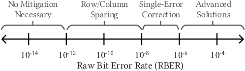
Error rates below are generally considered to be safe for normal operation and do not require mitigation [434, 321]. Relatively low error rates up to are addressed using row and column sparing, where memory designers provision extra rows and/or columns of storage cells at design-time to serve as replacements for other rows and columns that contain erroneous cells [276, 384, 434, 538, 212]. Higher error rates up to may be treated using single-error correcting (SEC) error-correcting codes (ECC) [116] (e.g., Hamming codes [193]) that can detect and correct a limited number of errors throughout the memory device. Finally, even higher error rates of require more advanced error-mitigation solutions, such as stronger, more complex ECC (e.g., BCH [69, 210] or RS [489] codes), fine-granularity repair techniques [434, 321, 373, 366], or solutions that address specific types of errors (e.g., higher refresh rates to address refresh- [370, 571] or RowHammer-related [312, 30, 426] errors). Section 2.3 discusses error-mitigation mechanisms in greater detail.
Recently, DRAM manufacturers have begun using single-error correcting ECC (on-die ECC) [276, 405, 447, 448, 330, 331] to manage increasingly prevalent single-bit errors, which are generally the predominant type of error that manufacturers must contend with once their process technology is mature [405, 88, 538, 351]. On-die ECC operates entirely within the memory device to detect and correct errors, so its operations are invisible outside of the memory device. Internally, on-die ECC subdivides the physical memory into ECC words (typically 64 or 128 bits wide [435, 177, 229]) and is capable of correcting one error within each word.
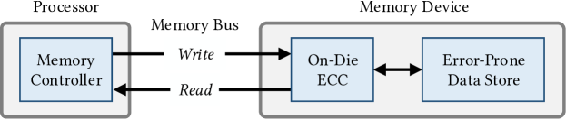
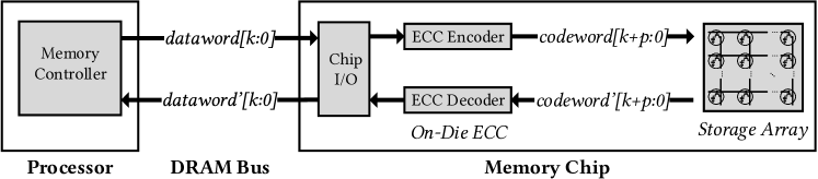
Figure 1.2 illustrates the high-level architecture of a system that uses a memory device equipped with on-die ECC. A memory controller within the processor interacts with the memory device over a memory bus. The memory controller issues read and write operations to load and store data to the memory. Within the memory device, we see that the load and store operations first interact with the on-die ECC logic, which then interacts with the physical data store that is susceptible to errors. To perform error detection and correction, on-die ECC encodes the data provided by the memory controller using an algorithm (e.g., Hamming encoding [193]) such that a decoding algorithm (e.g., syndrome decoding [409, 492]) can tell when one (or more, given a more complex coding algorithm) error(s) have occurred.
In this way, on-die ECC enables DRAM manufacturers to tolerate errors that are randomly distributed throughout the memory device, providing consumers with the appearance of a more reliable memory device without exposing the underlying reliability and error characteristics of the memory chips. In particular, manufacturers can preserve acceptable manufacturing yield at relatively low cost (i.e., 6.25-12.5% storage capacity [177] with low area, performance, and energy overheads [405, 276, 88]) using a simple single-error correcting ECC today [405, 253]. However, because on-die ECC is a key tool for DRAM manufacturers to manipulate factory yield, it is inherently tied to profitability and business interests [434]. Therefore, DRAM manufacturers treat the details of on-die ECC and the error rates it masks as proprietary, not disclosing them in publicly-available documentation (e.g., device datasheets).
1.1 Problem Discussion
Unfortunately, on-die ECC introduces new challenges for scientists and engineers (both researchers and practitioners in the field, in academia as well as industry) who need to understand memory reliability characteristics in the course of their work. This is because on-die ECC has a limited correction capability: although it can fully correct all single-bit error patterns, its behavior, when faced with multi-bit error patterns (i.e., uncorrectable error patterns), is undefined based on the particular ECC function used inside a given memory chip to correct the errors [538, 456, 258, 177]. As a result, on-die ECC obfuscates raw error patterns (i.e., the pre-correction errors) into unpredictable, implementation-dependent error patterns after on-die ECC correction (i.e., the post-correction errors).
Figure 1.2 explains why this is the case. Although the memory controller reads from and writes to the memory device, it has no visibility into the encoded data that is stored into the physical memory cells. Instead, it only has access to data that has already been modified by the on-die ECC mechanism. Therefore, the memory controller is entirely unaware when errors occur and/or are corrected by the on-die ECC logic. Similarly, when the on-die ECC logic faces uncorrectable errors, the memory controller simply receives the corrupted data returned by the DRAM chip without any indication that the on-die ECC logic was unable to correct the errors (if they were even detected at all) or even exacerbated the total number of errors through miscorrection [258, 119, 538]. As a result, the memory controller cannot easily reason about the errors that it observes, even if the physical processes that cause the errors to begin with (e.g., circuit-level models) are well understood.111Note that, even if the on-die ECC circuitry were not proprietary (i.e., its details were publicly known), the memory controller would still lack the visibility into the on-die ECC mechanism’s error-correction process because the mechanism provides no feedback to the memory controller when errors are detected and/or corrected.
On-die ECC’s error-correction properties are desirable during normal operation when uncorrectable errors are infrequent. However, its obfuscation of raw error characteristics severely impacts studies that seek to understand how errors occur in order to improve the system’s overall robustness (e.g., in terms of reliability, performance, security, safety, etc). We identify and discuss three concrete example consumer use-cases that are negatively impacted by the use of on-die ECC.
System design. System designers who integrate commodity memory chips into their designs must understand the chips’ reliability characteristics in order to create a system that meets their own design goals. Unfortunately, on-die ECC alters the memory chip’s reliability characteristics in a way that makes predicting the worst-case behavior difficult to anticipate: when faced with an uncorrectable error pattern, on-die ECC may act to exacerbate the error pattern into an even worse pattern, depending on the particular ECC function chosen by the memory manufacturer [538, 177, 258, 456, 466, 88]. This forces the system designer to make conservative assumptions about the worst-case reliability characteristics, often overprovisioning their own designs relative to what would be necessary if on-die ECC were not present [176, 88].
Third-party test and qualification. Test and qualification engineers exercise various operating conditions to determine whether a given memory chip satisfies design requirements [318, 319, 24, 20, 31]. If and when errors are observed, the engineer must often understand (i.e., debug) why the error occurred, a process known as root-cause analysis [20, 52]. Unfortunately, on-die ECC obfuscates the raw errors in a way that is opaque to the engineer. Upon observing an error, the engineer cannot easily determine the underlying cause for the error since the details of the error-correction process are contained within the memory chip and not visible to the engineer.
Memory error characterization. Scientists monitor and/or deliberately induce memory errors (e.g., by violating manufacturer-recommended operating timings [343, 346, 294, 295, 296, 550, 551, 91, 312, 369, 297], using extreme operating environments [138, 35, 580, 554, 168, 353], monitoring large-scale systems [54, 52, 74, 397, 529]) to understand how errors behave across a broad range of operating conditions. This process is known as error characterization and is generally performed with the goal of developing models and insights that can be used to build smarter systems and improve the technology itself. Unfortunately, on-die ECC conflates the technology-specific characteristics with the particular ECC circuitry used in a given memory chip [467]. Therefore, the results of an error characterization study no longer reliably reflect properties of the memory technology alone and are difficult to put into context alongside results from a memory device that uses a different on-die ECC mechanism.
All three use-cases suffer from the lack of transparency into DRAM error characteristics. In each case, not being able to understand and reason about the observed behavior limits the DRAM consumer’s ability to work with and improve upon DRAM chips that use on-die ECC. In Chapter 8, we take this observation further and argue that the more general lack of transparency into DRAM operation and reliability discourages system designers from innovating upon the DRAM substrate and adapting commodity DRAM chips to the unique needs of their particular systems.
The obfuscation that on-die ECC causes is expected to worsen as newer memory chips with higher error rates incorporate even stronger error-mitigation mechanisms that, in turn, may further obfuscate error characteristics. Thus, it is crucial to develop techniques that overcome this problem not only for today’s DRAM chips that incorporate on-die ECC, but also other memory technologies that are prevalent (e.g., NAND flash [401, 78, 74, 75]) and emerging (e.g., phase-change memory [339, 340, 632, 341, 481, 358, 598], magnetoresistive memories [144, 597, 110, 217, 29]) that will, or already do, require similar error mitigations.
1.2 Solution Direction
In this dissertation, we seek to (1) understand how on-die ECC obfuscates the underlying memory error characteristics; and (2) develop new testing techniques that scientists and engineers can use to overcome the obfuscation.
1.3 Thesis Statement
Our approach is encompassed by the following thesis statement:
The error characteristics that on-die ECC obfuscates can be recovered using new memory testing techniques that exploit the interaction between on-die ECC and the statistical characteristics of memory error mechanisms to expose physical cell behavior, thereby enabling scientists and engineers to make informed decisions towards building smarter and more robust systems.
1.4 Our Approach
To identify and address the challenges that on-die ECC introduces, we (i) introduce a series of new testing techniques that enable scientists and engineers to make sense of the post-correction error characteristics that are visible outside of the memory chip in terms of the raw pre-correction errors that are hidden behind on-die ECC; and (ii) build a detailed understanding of how on-die ECC obfuscates raw error characteristics thorough a combination of experimental and analytical studies. We briefly review our new mechanisms and studies in the remainder of this section.
1.4.1 Understanding DRAM Data-Retention Error Profiling
Volatile DRAM cell storage capacitors naturally lose charge over time, resulting in data loss (i.e., data-retention errors) if the charge is not periodically restored (i.e., refreshed) [190, 369, 191].222Section 2.2.5 discusses the relevant circuit-level error mechanisms in greater detail. Unfortunately, periodically refreshing all DRAM cells (e.g., performed every 32 or 64 ms for modern DRAM [246, 249, 250]) incurs significant performance and energy overheads [370]. To overcome these overheads, prior works [370, 449, 582, 571, 366, 434, 165, 480, 241, 298, 300, 278, 468, 390] develop a variety of techniques to eliminate unnecessary refresh operations by exploiting the observation that only a small subset of all cells actually require frequent refreshing.
However, identifying these few cells is a difficult problem known as data-retention error profiling. We observe that prior works generally rely on a slow and expensive approach to profiling that we refer to as brute-force profiling. Brute-force profiling consists of iteratively writing data to DRAM, waiting for errors to occur, and reading the data back to identify possible errors. Unfortunately, this approach is too slow and is detrimental to system execution, especially when profiling may be continuously performed during run time.
To develop a faster, more efficient profiling algorithm, we perform a thorough experimental data-retention error characterization study of 368 LPDDR4 DRAM chips from across three major DRAM manufacturers. We closely examine how data-retention errors occur, both collectively and at an individual cell granularity. Based on our study, we identify three key metrics that define a complex tradeoff space surrounding data-retention error profiling: coverage, false positive rate, and runtime. We show that making concessions in one or more dimensions can enable benefits in the others.
We use this principle to propose reach profiling, a new profiling algorithm that searches for errors at a longer refresh interval and/or higher temperature relative to the desired operating conditions. In doing so, reach profiling identifies errors under conditions at which they are more likely to be observed, thereby both coverage and runtime at the cost of identifying false positives. Using experimental data, we show that our first implementation of reach profiling (called REAPER) can achieve on average of over 99% coverage with less than a 50% false positive rate while running 2.5 faster than the brute-force algorithm by profiling at 250 ms above the target refresh interval. Furthermore, our end-to-end evaluations show that REAPER enables significant system performance and DRAM power improvements, outperforming the brute-force approach and enabling larger reductions of the refresh overhead that were previously unreasonable to the profiling overheads.
1.4.2 Inferring On-Die ECC and Raw Error Characteristics
To understand how on-die ECC impacts data-retention error characterization studies, we study how the on-die ECC error correction process affects the statistical properties of data-retention errors. These properties are well understood based on extensive experimental studies performed throughout decades of literature [190, 191, 265, 264, 305, 323, 369, 300, 571, 480, 278, 468, 390, 467, 466, 589, 526, 590, 282, 284, 283, 285, 327, 491, 498, 138, 35, 580, 554, 168, 353, 199]. Unfortunately, as we show in this work, the errors observed after ECC correction no longer exhibit the expected statistical characteristics but rather depend on the particular on-die ECC implementation used in a given DRAM chip.
To better understand both on-die ECC and the raw error characteristics, we develop Error Inference (EIN), a new statistical inference methodology capable of inferring details of both aspects using only the processor-visible post-correction errors. EIN uses maximum a posteriori (MAP) estimation over statistical models that we develop to represent ECC operation to: (1) reverse-engineer the type and correction capability of on-die ECC; and (2) infer high-level statistical properties of the pre-correction errors (e.g., the raw bit error rate). As part of our work, we develop and release EINSim [4], a flexible open-source simulator that facilitates applying EIN to a wide variety of DRAM devices and standards.
We evaluate EIN through the first experimental data-retention error characterization study of DRAM devices with on-die ECC in open literature. We test 232 (82) LPDDR4 devices with (without) on-die ECC to demonstrate that EIN enables (1) reverse-engineering the type and strength of the on-die ECC implementation, which we find to be a single-error correcting Hamming code with {136 code, 128 data} bits; (2) inferring pre-correction data-retention error rates given only the post-correction errors; and (3) recovering the well-studied raw bit error distributions that on-die ECC obfuscates.
1.4.3 Determining On-Die ECC Implementation Details
To determine exactly how on-die ECC acts upon specific raw bit error patterns, we observe that data-retention errors are data-dependent (i.e., they only occur in cells programmed with specific data values). By programming specific cells to specific values, we can prevent those cells from experiencing errors. We exploit this capability to develop a new testing methodology, Bit-Exact Error Recovery (BEER), that systematically determines the exact mathematical function used for a given on-die ECC implementation (i.e., its parity-check matrix) without hardware tools, prerequisite knowledge about the DRAM chip or the on-die ECC mechanism, or access to ECC metadata (e.g., error syndromes, parity information). BEER extracts this information by using carefully-crafted test patterns that reveal behavior unique to a given ECC function when inducing data-retention errors.
We use BEER to identify the ECC functions of 80 real LPDDR4 DRAM chips that use on-die ECC from across three major DRAM manufacturers. We then evaluate BEER’s correctness in simulation and performance on a real system to show that BEER is both effective and practical when applied to a wide range of ECC functions. To show that BEER is useful in various settings, we introduce and discuss several concrete ways that DRAM consumers can use BEER to improve upon their design and test practices. In particular, we introduce Bit-Exact Error Profiling (BEEP), the first error profiling algorithm that uses the known on-die ECC function (e.g., via BEER) to recover the number and bit-exact locations of the unobservable raw bit errors responsible for a given observed uncorrectable error pattern.
1.4.4 Enabling Error Profiling in Memory That Uses On-Die ECC
Efficiently mitigating errors at high error rates (e.g., ) typically requires fine-grained repair strategies that focusing error-mitigation resources only on those bits that are susceptible to error (i.e., at-risk bits). However, these strategies require a fast and effective way to identify the at-risk bits. Unfortunately, on-die ECC obfuscates how the memory controller perceives errors, thereby complicating the process of identifying at-risk bits (i.e., error profiling).
To understand how on-die ECC impacts error profiling, we analytically study how on-die ECC operations alter the system’s view of memory errors. Based on our study, we find that on-die ECC introduces statistical dependence between errors that occur in different bits that would otherwise be uncorrelated. We observe that this dependence introduces three key challenges for error profiling: (1) a small set of probabilistic raw bit errors can give raise to a combinatorially large set of at-risk bits; (2) because the profiler cannot observe raw bit errors, it wastes significant testing time to explore various combinations of raw bit errors to determine whether a given bit is at-risk; and (3) inducing worst-case testing conditions requires identifying complex multi-bit worst-case test patterns, which are significantly harder to develop than single-bit worst-case test patterns.
To address these three challenges, we introduce Hybrid Active-Reactive Profiling (HARP), a new bit-granularity error profiling strategy that operates from within the memory controller to identify at-risk bits. HARP rapidly achieves high coverage by exploiting two key insights. First, uncorrectable errors have two key sources: (1) raw bit errors that pass through on-die ECC unmodified, referred to as direct errors; and (2) mistakenly “corrected” bits as a result of implementation-dependent undefined on-die ECC behavior, called indirect errors. Second, the number of indirect errors can never exceed the correction capability of the on-die ECC code. Therefore, the key idea of HARP is to separately identify bits that are at risk of direct and indirect errors: with small modifications to the on-die ECC logic, the memory controller can exploit an on-die ECC read bypass path to quickly and efficiently identify all bits at risk of direct errors. Then, the memory controller can safely capture any remaining bits at risk of indirect errors using a secondary ECC within the memory controller.
We evaluate HARP relative to two baseline profiling strategies that rely only on post-correction errors to identify at-risk bits. We find that HARP achieves 99th percentile coverage of at-risk bits in 20.6%/36.4%/52.9%/62.1% of the number of profiling rounds required by the best baseline strategy given 2/3/4/5 pre-correction errors. Based on our evaluations, we conclude that HARP effectively overcomes the three aforementioned profiling challenges introduced by the presence of on-die ECC.
1.4.5 Advocating for Transparent DRAM Reliability Characteristics
Finally, based on the insights we developed throughout our studies, we argue the importance of having transparency into basic commodity DRAM reliability characteristics. We observe that, although techniques exist for system designers to adapt commodity DRAM chips to their systems’ particular performance, energy, reliability, security, etc. needs (e.g., by implementing error-mitigation mechanisms [301, 86, 614, 563, 260, 302, 435, 261, 98, 102, 385, 470, 584], reducing refresh overheads [370, 449, 582, 571, 366, 434, 165, 480, 282, 284, 283, 285, 241, 298, 300, 278, 468, 390], optimizing access latency [89, 91, 294, 343, 346, 586, 627, 197, 326, 390]), implementing these techniques requires knowing key information related to DRAM reliability (e.g., details of the DRAM microarchitecture, testing best-practices). Unfortunately, this information is not available today through official channels. Therefore, system designers must rely on assuming or inferring this information through unofficial channels (e.g., reverse-engineering techniques), which poses a serious barrier to practical adoption of such optimizations [285, 479, 504].
We substantiate this argument through four concrete case studies: (1) improving system-level memory reliability; (2) reducing DRAM refresh overheads; (2) improving the DRAM access latency; and (3) implementing defense mechanisms against the RowHammer vulnerability. In each study, we find that implementing a solution based on previously-proposed mechanisms requires making restrictive, potentially incorrect assumptions about a given DRAM chip. We identify DRAM standards as the root of the problem: current standards rigidly enforce a fixed operating point with no specifications for how a system designer might explore alternative operating points.
To overcome this problem, we introduce a two-step approach that reevaluates DRAM standards with a focus on transparency of reliability characteristics. In the short term, we ask for information release through a combination of both (1) crowdsourced testing from DRAM consumers; and (2) official information from DRAM manufacturers, possibly standardized by extensions to DRAM standards. In the long term, we propose extending DRAM standards with explicit DRAM reliability standards that provide industry-standard guarantees, tools, and/or information that enable DRAM consumers to perform their own reliability analyses and understand DRAM reliability at different operating points.
1.5 Contributions
This dissertation makes the following contributions:
-
1.
We build a detailed understanding of how on-die ECC obfuscates the statistical characteristics of main memory error mechanisms. To our knowledge, ours is the first study to explore this problem in detail. In doing so, we introduce new statistical models to represent how pre-correction errors are transformed by on-die ECC and draw new insights concerning the challenges that on-die ECC introduces for understanding and mitigating errors. Chapters 4–7 describe how we build this understanding through studying basic data-retention error characteristics and how on-die ECC affects those characteristics from the perspective of the memory controller.
-
2.
We perform the first experimental characterization study of data-retention error characteristics in LPDDR4 DRAM chips in order to understand the complex tradeoffs inherent to data-retention error profiling. Using the results of our study, we introduce and evaluate reach profiling, a new error profiling strategy that improves coverage and performance relative to prior data-retention error profiling strategies. Chapter 4 describes our experimental study and reach profiling in detail.
-
3.
We perform the first experimental characterization study of DRAM chips with on-die ECC in order to understand how on-die ECC affects the memory controller’s perception of data-retention errors. We show that on-die ECC obfuscates expected statistical characteristics in a way that depends on the particular on-die ECC implementation. Based on these observations, we introduce Error Inference (EIN), a new statistical inference methodology for identifying key properties of the on-die ECC implementation (e.g., correction capability, word length) and pre-correction errors (e.g., error rate) by comparing the post-correction errors’ expected and observed statistical characteristics. Chapter 5 describes our experimental study and EIN in detail.
-
4.
We introduce BEER, the first testing methodology that identifies the full on-die ECC function (i.e., its parity-check matrix) without requiring hardware tools, prerequisite knowledge about the DRAM chip or on-die ECC mechanism, or access to ECC metadata (e.g., error syndromes, parity information). We use BEER to identify the ECC functions of real LPDDR4 DRAM chips and evaluate BEER both in simulation and on a real system to show that it is practical and effective. Chapter 6 describes BEER and its evaluations in detail.
-
5.
We introduce BEEP, a new DRAM data-retention error profiling methodology that leverages the information provided by BEER to infer the precise counts and bit-exact locations of raw bit errors that are responsible for an observed uncorrectable error pattern. We show that BEEP enables characterizing pre-correction error locations across different ECC functions, codeword lengths, error patterns, and error rates. Chapter 6 describes BEEP and its evaluations in detail.
-
6.
We analytically study how on-die ECC affects the systems’ view of uncorrectable errors in order to understand the effects that on-die ECC has on error profiling. Based on our study, we identify three key challenges that on-die ECC introduces for error profiling (discussed in detail in Chapter 7). We then introduce HARP, a new profiling strategy that overcomes the three challenges by leveraging the key insight that only a limited number of at-risk bits need to be identified in order to guarantee that all remaining at-risk bits can be safely identified. We evaluate HARP to show that it effectively overcomes the three challenges as compared with existing profiling strategies that rely only on observing post-correction errors. Chapter 7 describes our analysis and HARP in detail.
-
7.
Based on the insights developed in Contributions 1-6, we advocate for increased transparency into commodity DRAM reliability so that system designers can make informed design decisions when integrating DRAM chips. We support our argument with four concrete case studies: (1) improving overall DRAM reliability; (2) reducing DRAM refresh overheads; (3) improving DRAM access latency; and (4) integrating RowHammer defenses. Based on these studies, we identify DRAM standards as the root of the problem and propose a two-step plan for improving transparency going forward. Chapter 8 describes the importance of DRAM transparency and provides our recommendations for current and future commodity DRAM-based systems.
-
8.
We describe remaining challenges in overcoming the problems caused by hidden ECC mechanisms, and in a broader sense, the lack of transparency of DRAM reliability. Chapter 9 discusses these challenges, including extending the proposed techniques to other devices and systems, leveraging the techniques to enable more robust system design, designing alternative error-mitigation mechanisms to replace on-die ECC, and improving transparency into DRAM reliability and operation.
1.6 Outline
This dissertation is organized into 9 chapters. Chapter 2 gives relevant background information about DRAM operation, failure modes, and error mitigation. Chapter 3 discusses related works that address relevant problems in error profiling, characterization, and mitigation. Chapter 4 presents our experimental study of DRAM data-retention errors in chips without on-die ECC in addition to introducing and evaluating reach profiling. Chapter 5 introduces EIN and its experimental evaluation using DRAM chips that use on-die ECC. Chapter 6 introduces BEER and BEEP and their respective evaluations. Chapter 7 introduces HARP and its evaluations. Chapter 8 discusses the value of having transparent DRAM reliability characteristics and argues for improved transparency going forward. Finally, Chapter 9 provides a summary of this dissertation as well as future research direction and concluding remarks.
?chaptername? 2 Background
In this chapter, we provide the necessary overview of the background material necessary to understand our discussions, analyses and contributions. Section 2.1 reviews DRAM organization and operation. Section 2.2 reviews key DRAM failure modes that are relevant to our work. Section 2.3 reviews memory error mitigation techniques. Section LABEL:bg:sec:block_coding provides an overview of block coding, the algorithm used for typical memory error-correcting codes. Finally, Section LABEL:bg:sec:sat_solver introduces boolean satisfiability (SAT) solvers as used in our work in Chapters 6 and 7.
2.1 DRAM Overview
This section describes DRAM organization and operation as relevant to this dissertation.
2.1.1 DRAM Organization
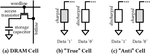
DRAM stores each bit of data in its own DRAM cell, as illustrated in Figure 2.1. The cell comprises a storage capacitor that encodes the binary data value using the charge level of the capacitor and an access transistor that is used to read and modify the stored data. The access transistor’s gate is manipulated by a control signal known as the wordline. When the wordline is enabled, the storage capacitor is connected to the bitline, so the charge stored in the storage capacitor equalizes with that in the bitline. Whether the capacitor encodes data ‘1’ or data ‘0’ as the charged state is an arbitrary convention and depends on the manufacturer’s particular circuit design. A cell that encodes data ‘1’ using the charged state is referred to as a ‘true cell’ and the discharged state as an ‘anti cell’ [327, 369, 599, 310].
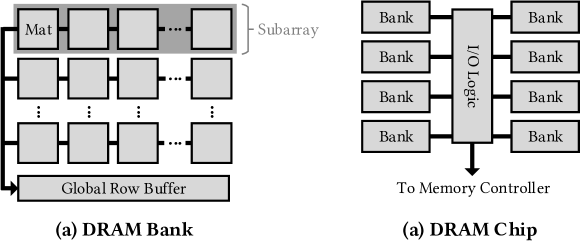
A DRAM mat stores multiple bits of data by organizing DRAM cells into a two-dimensional grid of rows and columns (typically 512-1024 cells per dimension). Figure 2.2 shows the architecture of a typical DRAM mat. A common wordline connects the gates of all access transistors of the cells along a row. Therefore, when a wordline is asserted (i.e., driven to logic ‘1’), all cells along the row are enabled. The drains of all access transistors along a column are connected by a common bitline. Each bitline is connected to a sense amplifier, whose circuits detect a small voltage shift on the bitline (i.e., as a result of charge sharing between the storage capacitor and the bitline) and amplify it to a CMOS-readable value. In this way, when a wordline is asserted, each cell along the row shares its capacitor’s charge with its respective bitline. Each bitline’s sense amplifier then detects and amplifies this shift, effectively reading the value stored in each cell along the row. Note that this process is destructive: once the value stored in a cell capacitor is read out, the storage capacitor no longer stores the original data. Therefore, the sense amplifier must recharge the cell following the read process in order to restore the correct data value before attempting a subsequent read. The sense amplifier can be thought of as temporarily caching the row’s data during the read operation, so the sense amplifiers are collectively referred to as a local row buffer.
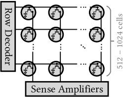
Figure 2.3a illustrates how mats are in turn organized into a grid to form a DRAM bank. Each bank typically comprises 32K-256K rows and 512-2K columns. Note that a row of mats is sometimes referred to as a subarray. Each bank contains a single global row buffer that is shared among all mats for I/O operations when the bank is read from or written to. Figure 2.3b shows how multiple DRAM banks are then combined to form a DRAM chip. Depending on the DRAM standard, each chip may comprise 8 [246] or 16 [249] banks.
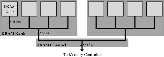
Similarly, depending on the DRAM standard, multiple chips may be combined to form a single interface, known as a channel, with the memory controller. Mobile DRAM (e.g., LPDDRn [250]) typically uses a single DRAM chip per channel, while desktop DRAM (e.g., DDRn [246, 249]) typically aggregates 4-16 DRAM chips to form a rank that connects to the channel. In general, up to eight ranks may time-multiplex the same channel. Figure 2.4 illustrates an example of a typical dual-rank DDR4 system with four DRAM chips per rank. The figure illustrates how each chip provides a 16-bit interface that is concatenated with all other chips in the rank to form a 64-bit rank interface. The two 64-bit rank interfaces then communicate with the memory controller by time-multiplexing the channel. Note that the DRAM channel also transfers command and address information to each chip in addition to the 64-bit data (not illustrated for simplicity).
2.1.2 DRAM Addressing
Accessing data at a given DRAM location is done by specifying its rank, bank, row, and column address. The rank address specifies which DRAM rank the channel should communicate with in order to access the data. The bank, row, and column addresses are broadcast to all chips within the target rank. The resulting data is then concatenated across all chips and returned to the memory controller over the channel.
DRAM manufacturers are not required to maintain a direct mapping between the row or column addresses provided on the bus and the physical location of the corresponding cell.111This is unrelated to the virtual and physical addresses that the system software deals with. The DRAM bus address is created by the memory controller as a function of the physical address that is determined by the system’s virtual-to-physical memory address translation process. Therefore, the system’s physical address is orthogonal to the DRAM’s internal address mapping for locating physical cells in the DRAM device. This means that manufacturers are free to shuffle rows and columns as desired to optimize their circuit designs. This mapping is generally irrelevant to the system software since there is no perceived difference between physical cells at different locations in the memory. Unfortunately, the mapping becomes relevant in the presence of reliability issues such as RowHammer [312, 297, 488] because the physical locations of errors depend on the physical locations that have been accessed. If the bus-to-physical address mapping is not known, it is difficult to determine where errors might have occurred.
Prior works [346, 583, 51, 267, 297, 555, 294] develop techniques to reverse-engineer the DRAM internal row and/or column mappings by deliberately inducing errors and observing their bus address locations. Knowing that the induced errors should follow well-understood characteristics based on the physical chip design (e.g., RowHammer errors should occur in rows that are physically adjacent to accessed rows), these works are able to infer the internal row and/or column organization. In Chapter 8, we argue that this information should be made public given that (1) it is helpful for researchers and engineers to know in order to design DRAM optimizations and security defenses; and (2) it can already be reverse-engineered, as shown by the aforementioned works.
2.1.3 DRAM Operation
The memory controller is responsible for orchestrating all DRAM operations, including DRAM initialization, access, and maintenance (e.g., periodic refresh and calibration). These operations are invoked through the use of DRAM commands, and DRAM manufacturers clearly specify the timing constraints surrounding their usage [246, 249, 250, 253, 254]. In this section, we briefly introduce the history of DRAM specifications in order to provide context for how they came about. Then, we discuss the primary commands and timings concerning DRAM access and refresh as mandated by modern JEDEC standards.
DRAM Specifications
Following the conception of single-transistor DRAM by IBM in the late 1960s [387, 439, 9, 132, 133], the first commodity DRAM chips (e.g., Intel 1103 [226], Mostek MK4096 [412]) quickly gained popularity due to their cost-per-capacity advantages relative to other viable main memory technologies [150]. Through the following decades, various manufacturers developed their own DRAM chips, resulting in a proliferation of different DRAM types and access protocols (e.g., FPM, EDO) that steadily improved storage density through continued improvements in both design and manufacturing. Several competing DRAM standards arose in the 1990s, including Intel’s PCx [225], Rambus’ RDRAM [486], and JEDEC’s SDRAM [245] standards. However, by the late 1990s, JEDEC thoroughly secured market dominance, effectively crowding out competing standards by the mid 2000s [87]. By the advent of modern DDRn memory, JEDEC had established significant barriers to entry for all non-JEDEC-compliant chips [87, 143].
Today, all major commodity DRAM manufacturers comply with JEDEC standards for DRAM interfaces and operating characteristics because JEDEC-compliance guarantees interoperability between DRAM chips and other JEDEC-compliant systems [244]. JEDEC DRAM standards are collectively developed by committees comprising both DRAM manufacturers and customers. Each specification discusses requirements for customer-visible aspects of a DRAM chip’s design, including features, electrical characteristics, access protocols, recommended operating conditions (e.g., timings, voltage, temperature). This enables a separation of concerns between DRAM manufacturers and consumers. In the ideal case, DRAM specifications are synonymous with customer requirements: DRAM manufacturers can focus on manufacturing the best possible DRAM chips that conform to the specification.
DRAM Access
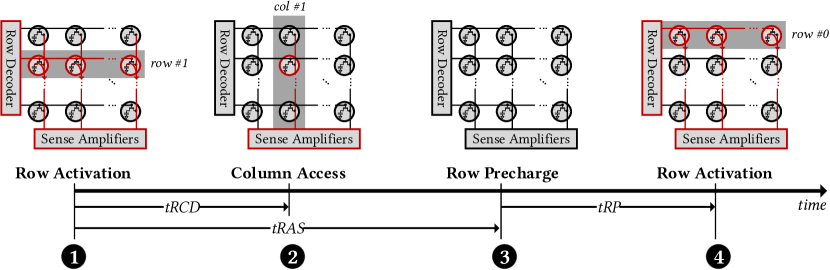
DRAM specifications outline the precise command sequence used for each DRAM access. As described in Section 2.1.1, each bank contains only one global row buffer. Therefore, only one row may be read from any given bank at a time. To meet this constraint, each DRAM access requires up to three operations:
-
1.
Row activation (ACT): The ACT command activates a row within a bank by asserting the row’s wordline and allowing the sense amplifiers to develop to CMOS-readable voltage values. This is referred to as opening the row.
-
2.
Column access (RD and WR): RD and WR commands read and write to a given column within the open row. The definition of a column depends on the DRAM geometry and standard, but typically refers to a 16-64-byte aligned region of the open row. While a given row is open, the memory controller is free to issue as many RD and WR commands as necessary to columns within the open row.
-
3.
Bank precharge (PRE): The PRE command precharges the currently open row within a bank by de-asserting the wordline and resetting all bitlines to their quiescent states (typically ). This prepares the bank for the next row activation.
Figure 2.5 summarizes the timing constraints that the memory controller must obey when issuing ACT, RD and WR, and PRE commands in the context of a DRAM read access. DRAM chip datasheets provide manufacturer-recommended values for each of these timings, in addition to many other timings for other commands.222We refer the reader to the JEDEC DRAM specifications for a more detailed overview of standardized DRAM commands and timings [246, 249, 250, 253, 254]. First, a new row (e.g., row address 1) in the bank is activated. This causes the row decoder to activate the row’s wordline, allowing the sense amplifiers to detect and amplify the row’s stored data values. Next, a particular column (e.g., column address 1) in the newly-opened row is accessed following a time delay of tRCD. Peripheral I/O logic (not illustrated) will transfer the corresponding data to the chip’s external interface. Then, the bank is precharged in order to close the open row and prepare the bank for the next row access. The PRE command may not be issued until at least tRAS has elapsed since the row activation. Finally, another row may be opened (e.g., row address 0) following tRP after the precharge operation.
DRAM Refresh
For as long as commodity DRAM has existed, the DRAM refresh algorithm has favored simplicity and correctness: the memory controller issues a fixed number of refresh commands every refresh window (tREFW), which corresponds to the retention time of the worst-case cell in the memory chip. The refresh algorithm guarantees that every DRAM cell is refreshed at least as often as required to prevent data loss,333This is true whether each refresh operation operates on all DRAM rows (e.g., burst-mode refresh [404]) or on a subset of all rows (e.g., distributed-mode refresh [404], fine-grained refresh [249]). and its simplicity means that both DRAM manufacturers and system designers can treat the refresh algorithm as a fixed design constraint without needing further specification.
Current DRAM specifications [246, 249, 253, 250, 254] mandate that the memory controller issue REF commands every 3.9-7.8s. Each refresh operation invokes dedicated refresh circuitry within the DRAM chip that refreshes a small number (e.g., 32) of rows. Throughout each tREFW period (i.e., 32-64ms), all rows in the DRAM chip are refreshed once.444Note that, while this is the common understanding, DRAM specifications do not mandate that internal refresh operations refresh all rows exactly once within tREFW. By adjusting the number of rows refreshed with each REF command, DRAM manufacturers may adjust the effective refresh rate for each row according to their needs in a manner that is invisible to the memory controller. However, it is important to note that different cells can withstand different refresh rates, and refreshing all cells at a fixed rate is a conservative strategy that accounts for the worst-case cell under worst-case operating conditions. As we will see in Chapter 4, this implies that there is significant room for improvement in the DRAM refresh algorithm.
2.1.4 Violating Recommended Timings
We can induce errors in real DRAM chips by deliberately violating manufacturer-recommended timings. The resulting error distributions allow us to: 1) reverse-engineer various proprietary DRAM microarchitectural characteristics [267, 343, 467, 91, 415, 295, 327, 294, 455, 198] and 2) understand the behavior of different DRAM errors (e.g., data retention [191, 369, 571, 370, 480, 282], access latency-related errors [295, 296, 551, 552, 159, 452]).
By increasing , we observe data-retention errors in certain cells with higher charge leakage rates [571, 191, 370, 276, 305, 190, 369, 434, 282, 283, 285, 589, 266, 264, 305, 323, 364]. The quantity and locations of these errors depend on i) the data pattern programmed into cells, ii) the layout of true- and anti-cells in DRAM [369, 327], and iii) environmental factors such as operating temperature and voltage [191, 370, 369, 282, 468, 94, 283, 284, 312, 354, 362, 285]. Section 2.2 discusses the statistical characteristics of data-retention errors in greater depth.
2.2 DRAM Errors and Failure Modes
In this section, we first clarify the terminology used throughout this dissertation to refer to memory errors. Then, we review three key DRAM failure modes that are relevant to our work: (1) DRAM data retention; (2) DRAM access timing violations; and (3) RowHammer.
2.2.1 Reliability-Related Terminology
We observe that different works use different terms to refer to related reliability concepts. Therefore, we clarify the reliability-related terms that we use throughout this dissertation.
Faults, Errors, and Failures
We use the terms fault, error, and failure according to the ISO/IEC/IEEE 24765 standard [221] as follows:
-
•
Fault: A defect in a hardware device or component.
-
•
Error: A discrepancy between the computed, observed, or measured value and the theoretically correct value.
-
•
Failure: The termination of the ability of a product to perform its required function.
Therefore, we use the term error to refer to bit-flips observed during testing and fault or error mechanism to refer to the underlying reason for an observed error (e.g., excessive charge leakage, electrical coupling between circuit components). Finally, we use the term failure mode when describing the manifestation of an error from the perspective of the rest of the system.
Types of Faults and Errors
Following from prior work [177, 258], we classify DRAM faults as inherent or operational. Inherent faults are caused by aspects of the DRAM technology and broadly encompass scaling-related faults such as data-retention and RowHammer. Operational faults are those that can cause errors during normal operation and include factors such as aging effects [252] and particle strikes [391]. Section 2.2.2 discusses both classes of faults in greater detail.
We refer to errors that occur within the physical memory device as raw errors or pre-correction errors to distinguish that they have not yet gone through error-correction logic. Similarly, we refer to errors that have gone through error correction (e.g., through on-die ECC) as post-correction errors. Note that all post-correction errors are the result of the error-correction mechanism being unable to fully correct an uncorrectable raw error pattern. Therefore, post-correction errors are either detectable-but-uncorrectable (DUE) errors or silent data corruption (SDC) errors. Given that on-die ECC is a single-error correcting code [447, 448, 330, 332, 405, 229, 253, 276, 466] that has no additional error-detection capability and does not report error detection or correction events to the memory controller, all post-correction errors we work with in this dissertation can be considered SDCs.
2.2.2 Key DRAM Failure Modes
DRAM suffers from a broad range of error mechanisms that can lead to different types of errors. Our work focuses primarily on errors that result from inherent faults due to DRAM technology scaling and deliberate violations of recommended operating timings and conditions (e.g., data-retention errors [190, 191, 571, 369, 35, 588, 607], errors due to access timing violations [294, 347, 343, 346, 91, 452, 326, 89]). In this section, we review key DRAM failure modes to provide context for our studies.
2.2.3 Manufacturing-Time Faults
Manufacturing-time faults include any defects incurred at manufacturing time that cause one or more DRAM cells to not meet design requirements. These faults can cause errors occur due to a variety of DRAM-specific (e.g., RowHammer [312, 422, 426, 576, 611, 460, 297], data-retention [190, 191, 571, 369, 35, 588, 607], variable-retention time [35, 286, 480, 608, 491, 526, 290, 291, 329, 410, 450, 282, 276, 369]) and non-specific (e.g., stuck-at faults due to manufacturing defects [20, 212, 414]) error mechanisms and are the primary reliability concern with DRAM technology scaling [405, 276, 177, 88, 434, 461, 420]. These errors are dealt with by manufacturers using on-die error-mitigation mechanisms, including row and column sparing [212, 88, 276, 434, 279, 538, 332], on-die ECC [447, 448, 330, 332, 405, 229, 253, 276, 466], and RowHammer-prevention logic (e.g., on-die target row refresh [198, 154, 243, 386]). Therefore, assuming the error mitigation mechanisms work as intended, these errors are normally unknown to the end user and are considered proprietary information by DRAM manufacturers [176, 434, 504, 479, 374, 147].
Prior works [176, 434, 297] explain that these errors become worse with continued process technology scaling because manufacturing variations between components become more significant as the components themselves shrink. For example, shrinking cell storage capacitors means that they will hold less charge and therefore be more sensitive to various charge leakage mechanisms [276, 434]. Therefore, as DRAM technology continues to scale, a larger proportion of cells fail to meet design targets and require error mitigation.
When deliberately changing access and refresh timings (e.g., during testing or custom operation), the user effectively chooses to operate under conditions that DRAM manufacturers did not design for. At these conditions, the on-die error mitigations that manufacturers provisioned to address manufacturing-time errors (e.g., errors related to data retention and access timings) no longer hide all errors, allowing the user to study their characteristics. Many prior works [268, 190, 191, 608, 526, 589, 269, 590, 37, 282, 369, 480, 571, 199, 94, 346, 510, 541, 267, 284, 283, 480, 546, 90, 344, 89, 91, 343, 295, 294, 296, 550, 551, 312, 311, 159, 305, 297] use this approach to observe scaling-related errors and understand their characteristics in order to develop more robust systems Section 3.3 reviews these studies in more detail.
2.2.4 Operational Failures
DRAM suffers from various faults that are prevalent among general semiconductor devices [252], including possible circuit-level aging effects [252, 397] and random external events (e.g., particle strikes [391]). Unfortunately, the details of commodity DRAM failure rates are proprietary [176, 434, 504, 479, 374, 147] and prior studies [510, 220, 541, 540, 542, 397, 54, 529] have had to conduct their own large-scale experimental analyses to estimate failure rates. These studies do not know the underlying faults responsible for an observed failure; instead, they infer reasons for the failures based on how the failures appear to the system (e.g., correlations between memory addresses) [52]. Therefore, the failure rates observed by these studies represent the cumulative effect of whichever circuit-level error mechanisms are dominant for the systems’ particular configurations.
Systems that need long-term resilience against operational failures typically incorporate additional error-mitigation mechanisms outside the DRAM chip (e.g., rank-level ECC within the memory controller [88, 301]). These mechanisms are better equipped to deal with operational failures because they are not as resource-constrained as the DRAM die. Therefore, they can provision resources to mitigate a wide variety of errors, including multi-bit errors and even failures of entire DRAM chips [301]. Section 2.3.3 discusses these mechanisms in more detail.
2.2.5 DRAM Data Retention Errors
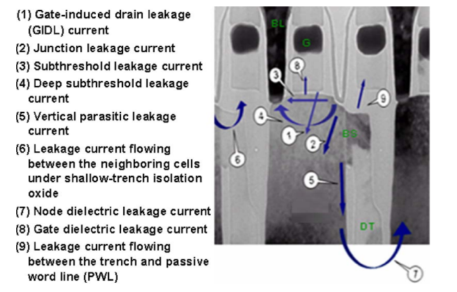
DRAM cell storage capacitors are susceptible to a large number of charge leakage mechanisms that vary in strength depending on the data values stored in cells, switching activity nearby a given cell, and with environmental factors such as temperature and voltage [95, 491, 191, 223, 342]. Figure 2.6 shows a cross-sectional view of a DRAM cell capacitor (illustrated as “DT”) alongside various charge leakage paths that it is susceptible to. The dominant leakage path(s) vary depending on the particular DRAM circuit design and operating conditions; however, all DRAM cells are susceptible to charge leakage and rely on periodic DRAM refresh operations to prevent data loss. At manufacturer-recommended operating conditions, DRAM refresh operations occur frequently enough to prevent data-retention errors from appearing.
However, when the memory controller deliberately reduces the frequency of refresh operations (e.g., in order to improve system performance and energy-efficiency [571, 370]) certain cells with worse leakage characteristics exhibit errors. Prior work [571, 190, 449, 191, 370, 601, 369, 282] has extensively studied how long different DRAM cells can correctly retain data (i.e., their retention times) and shown that only a small set of worst-case cells actually require frequent refreshing (i.e., at the JEDEC-standardized rate of 32-64 ms [246, 249, 250]). In contrast, the vast majority of cells have much longer retention times (e.g., s). This high cell-to-cell variation is a result of manufacturing process variation and is becoming worse with continued technology shrinkage [434, 88, 211].
Through their experimental studies, prior works [190, 191, 369, 571, 370, 264, 589, 323] have identified several key characteristics of DRAM data-retention errors that are essential to our work in this dissertation.
First, data-retention errors are strongly dependent on and can be easily induced by manipulating the refresh window (e.g., using configuration registers within the memory controller [28]). Except for certain cells that are susceptible to a phenomenon known as variable retention time (discussed later in this section), most strong DRAM cells exhibit relatively stable retention times and fail repeatably when the refresh window exceeds a cell’s retention time.
Second, data-retention errors are uncorrelated and occur uniform-randomly throughout the memory device as a result of random process variation. Prior works demonstrate this property through extensive error-characterization studies, showing that data-retention errors exhibit no discernible spatial patterns [191, 370, 37, 571, 526] and can be realistically modeled as uniform-randomly distributed [295, 526, 37] independent events [526].
Third, data-retention errors are data-dependent, occurring only in cells whose storage capacitors are in the charged state. This means that only true-cells programmed to data ‘1’ are likely to fail, and vice-versa for anti-cells. This behavior has been observed across DRAM chips from a broad range of manufacturers and standards [327, 369, 599, 310], and we hypothesize this is due to the dominant leakage modes causing charge to drain the storage capacitor rather than to charge it.
Variable Retention Time
Certain cells are vulnerable to an error mechanism known as variable retention time (VRT), where a cell unpredictably switches between two or more distinct retention times states [35, 286, 480, 608, 491, 526, 290, 291, 329, 410, 450, 282, 276, 369]. This affects the cell’s data-retention error characteristics because the likelihood that a cell fails changes over time depending on its retention time state. Prior works [405, 276, 88] identify VRT errors as a key DRAM scaling challenge, and on-die ECC is partially motivated by their presence. Although techniques for identifying and mitigating VRT-related errors have been proposed [480, 523], efficiently identifying and mitigating VRT errors remains a difficult problem.
2.2.6 DRAM Access Timing Violations
The memory controller may deliberately choose to violate the manufacturer-recommended inter-command timings in order to improve DRAM access performance [89, 91, 294, 343, 346, 586, 627, 197, 326, 390, 620, 344, 90] or exploit beneficial side effects of the resulting undefined behavior (e.g., to generate random values [550, 296, 452] and device fingerprints [551, 295], perform logic operations [159, 451, 518, 516, 513, 514]). However, if timings are violated beyond what a given DRAM chip can withstand, errors may occur due to internal DRAM circuitry (e.g., sense amplifiers, peripheral logic) having insufficient time to complete necessary operations. We briefly discuss activation- and precharge-related errors because they have been extensively studied and exploited by prior works.
Activation-Related Errors
Reducing the time given for DRAM row activation (i.e., tRCD) can cause errors due to reading out data from the row buffer before the sense amplifiers are able to fully develop to CMOS-readable values [91]. Several works study the effects of reducing tRCD and find that (1) more errors occur with greater timing violation [89, 91, 294, 295, 343, 199]; (2) many of the resulting errors tend to cluster along bitlines [91, 294, 296]; and (3) errors are more likely to occur closer to one edge of a given subarray [346]. These observations are all consistent with sense amplifier behavior: with lower tRCD, the sense amplifier has less time to develop, thereby becoming more likely to yield incorrect data. In particular, due to manufacturing process variation, certain sense amplifiers develop more slowly than others, causing them to exhibit errors for all cells along their respective bitline. Furthermore, cells that are physically further away from the sense amplifier (e.g., on the other side of the bitline) experience a longer signal propagation delay after wordline activation before their bitline perturbation arrives at the sense amplifier, introducing asymmetry between different cells along the same bitline.
Precharge-Related Errors
Reducing the time given for a bank to precharge a row (i.e., tRP) can cause errors because all bitlines may not be fully precharged to their quiescent state, thereby disturbing the sensing process for the following row activation. Several works [89, 343, 91, 346, 551, 550] study how precharge-related errors manifest, finding that (1) overall error rates increase sharply as tRP is reduced [343, 91, 551]; (2) precharge-related errors are more likely to occur near the boundaries of mats [346]; and (3) at extremely high error rates that are observed when aggressively reducing tRP, errors appear to occur roughly uniform-randomly [551]. Similar to the case with activation-related errors, these observations can be explained by a combination of design-dependence and manufacturing process variation. When errors begin to appear, they cluster near the edges of mats, where the signal propagation delay from the precharge signal drivers and row decoders to the cells is greatest. In the extreme case, when tRP is very short, the design-dependence is subsumed by cell-to-cell variation causing random cells to be more susceptible to error than others.
2.2.7 RowHammer
RowHammer [312, 38, 422, 426] is a failure mode in which repeated accesses to a given DRAM row (known as an aggressor row) can induce bit-flips in physically nearby rows (known as victim rows). RowHammer can be classified as a read-disturb fault, and prior works [611, 577, 263, 288, 36, 488] identify two circuit-level charge leakage mechanisms that contribute towards RowHammer errors: (1) electron migration; and (2) capacitative crosstalk. As with data-retention errors, the strengths of each of these error mechanisms varies greatly between DRAM chip designs and with operating conditions, and significant research effort [312, 297, 422, 426, 459, 460, 611, 113, 577, 198, 606, 36] has been expended to understand how RowHammer errors behave. Based on this understanding, many works [19, 30, 34, 312, 288, 537, 348, 616, 520, 567, 325, 462, 604, 273, 39, 41, 42, 71, 172, 196, 136, 496, 609, 610, 160, 603, 181, 386, 311, 249] have proposed defense mechanisms ranging from the device- to system-level.
2.3 Memory Error-Mitigation Mechanisms
This section provides an overview of error-mitigation mechanisms that are commonly used in memory hardware design, including those that operate within the memory die and in the memory controller.
2.3.1 Row and Column Sparing
DRAM manufacturers have long since provisioned extra rows and columns within storage arrays in order to provide replacements in the event that some are defective [212, 88, 276, 434, 279, 538, 332]. This is known as row and column sparing and helps DRAM manufacturers tolerate imperfections during manufacturing, thereby improving manufacturing yield at a modest expense of chip area resources. Each manufacturer evaluates the tradeoffs involved based on their own designs, manufacturing processes, and business goals in order to determine how many spare rows and columns to provision. Several works [88, 276, 434, 538] argue that current inherent DRAM error rates have surpassed the correction capability of row and column sparing alone, necessitating solutions such as on-die ECC, or even stronger mechanisms. In general, the exact error rates and spare element counts are proprietary and vary between manufacturers [434, 176].
2.3.2 On-Die ECC
For single-bit error rates that are too expensive to mitigate using row and column sparing, DRAM manufacturers have turned to on-die ECC as a solution [435, 405, 276, 448, 176, 538, 447, 330, 332, 467, 466, 464]. Because on-die ECC operations happen within a DRAM die that is not optimized for general logic operations, keeping on-die ECC simple and efficient is a primary design goal [88, 332]. Therefore, DRAM manufacturers today use simple single-error correcting Hamming codes [193] that operate on data chunks of 64 [229] or 128 [447, 448, 330, 331] bits.
Figure 2.7 illustrates a simple example where a memory controller interfaces with a single memory chip that uses on-die ECC. On a write operation, the memory controller writes a -bit dataword to the memory device. Internally, the memory device encodes the data into a -bit codeword before writing it to the physical storage array. On a read operation, the data that the memory controller receives is first decoded by the ECC logic from a -bit codeword’ (where the ”‘ indicates that the codeword may contain errors) into a a -bit dataword’. In this way, the memory controller observes only the post-correction errors and has no visibility whatsoever into how the ECC encoding and decoding mechanism operates. Section LABEL:subsec:ecc_bg provides an overview of the mathematical operation of on-die ECC.
The details of the on-die ECC implementation are considered proprietary secrets because they, like row and column sparing, are tied to a manufacturer’s factory yield rates [224, 105], which are in turn directly connected to business interests, potential legal concerns, and competitiveness in a USD 45+ billion DRAM market [482, 572]. Therefore, DRAM manufacturers do not disclose these details in public documentation. Furthermore, in our experience, they are unwilling to reveal on-die ECC details under confidentiality agreements, even for high-volume customers for whom knowing the details can be mutually beneficial.555Even if such agreements were possible, they would likely be possible only for parties with large stakes in the DRAM industry. The majority of DRAM consumers (e.g., smaller industry teams, academics) who do not have close relations with DRAM manufacturers will be unlikely to forge such agreements.
2.3.3 Rank-Level ECC
Row and column sparing and on-die ECC are unsuitable for addressing high error rates (e.g., ) and multi-bit errors (e.g., burst errors, component-level failures) [434, 373, 276]. For high-reliability systems (e.g., large-scale clusters) that need to be resilient against such errors, system designers typically integrate an ECC mechanism within the memory controller, referred to as rank-level ECC [301, 177, 435]. Rank-level ECC uses data blocks at the granularity of the DRAM interface (or larger) to provide stronger error correction than on-die ECC can feasibly provide. This section reviews major types of rank-level ECC designs that provide varying degrees of reliability.
SECDED ECC
Single error correcting, double error detecting (SECDED) ECC is a simple but prevalent rank-level ECC solution [301]. This scheme interfaces with DRAM using 72 total bits per transfer, 8 of which are metadata used for error detection and correction (i.e., a 72,64 extended Hamming code). SECDED ECC is capable of correction one error and detecting two errors within each 72-bit transfer.
Chipkill ECC
Chipkill ECC maps ECC words to DRAM chips in a way that allows tolerating the failure of one or more entire DRAM chips within a rank. Several approaches to chipkill ECC exist, including interleaving SECDED codes [129], using Reed-Solomon (RS) codes [489] with symbol sizes that are aligned with entire DRAM chips (e.g., 4 bits/symbol when using DRAM chips with 4-bit interfaces [26], 8 bits/symbol mapped across two transfers from DRAM chips with 4-bit interfaces [27]). However, many of these schemes require datawords that are longer than the 64-bit interface, which incurs additional reliability challenges due to some interface-related errors occurring multiple times at the same interface bit positions [301].
Other System-Level ECC Designs
Other rank-level ECC designs have been proposed [301, 614, 563, 260, 302, 178, 100, 303, 383, 98, 621, 612, 99, 385, 625, 101] to both enhance reliability and overcome limitations of existing schemes. In general, each design provides a different tradeoff between reliability and resource consumption, and it is ultimately up to the system designer to decide which solution is most appropriate for their design goals.
2.3.4 Repair Mechanisms
As memory manufacturers continue to improve storage density, they exacerbate various technology-specific error mechanisms that then increase error rates. A broad class of techniques referred to as repair mechanisms identify and repair bits that are at risk of error from within the memory controller in order to mitigate high error rates (e.g., ) that are infeasible to mitigate using traditional ECC-based methods [320, 373, 321, 434, 366, 480]. Prior works [366, 434, 321, 373, 320, 507, 432, 622, 581, 289] propose a variety of repair mechanisms for both DRAM and emerging memory technologies.
Repair Granularity
Repair mechanisms [212, 615, 434, 231, 507, 366, 556, 320, 373, 321, 511, 594, 384, 538, 294, 346] perform repair at granularities ranging from kilobytes to single bits. The granularity at which a repair mechanism identifies at-risk locations is its profiling granularity. For example, on-die row and column sparing [249, 253, 276, 384, 434, 538, 212, 88] requires identifying at-risk locations at (or finer than) the granularity of a single memory row. Table LABEL:tab:categorization categorizes key repair mechanisms based their profiling granularities. In general, coarse-grained repair requires less intrusive changes to the system datapath because repair operations can align with data blocks in the datapath (e.g., DRAM rows, cache lines, processor words). However, this means that the repair mechanism suffers from more internal fragmentation because each repair operation sacrifices more memory capacity regardless of how few bits are actually at risk of error.
?chaptername? 3 Related Work
Many prior works study DRAM errors and develop techniques for understanding and mitigating memory errors. This section provides an overview of closely-related works.
3.1 Studying and Improving On-Die ECC
Developing an on-die ECC design that provides the benefits of highly-efficient on-die error correction without introducing additional challenges for the rest of the system is a complex problem involving the interests of both DRAM manufacturers and consumers. This section reviews general techniques for exposing ECC mechanisms and recent works that approach the on-die ECC design problem in different ways.
3.1.1 Reverse-Engineering ECC Mechanisms
Both EIN (Chapter 5) and BEER (Chapter 6) are capable of reverse-engineering details of a given on-die ECC implementation. Several works provide techniques to reverse-engineer details of the ECC mechanisms used in NAND flash memory [568, 569, 596] and DRAM rank-level ECC [115]. However, each of these techniques require some amount of visibility into the ECC mechanism. These works rely on either directly observing the encoded data (i.e., the codewords) using a side-channel [115], bypassing ECC and directly probing the raw memory [568, 569, 596, 115], or knowing when ECC performs an error-correction operation (e.g., by observing the change in memory access latency when ECC performs a correction operation [115, 180], or using custom driver software [115]).
However, on-die ECC is fully contained within the memory die and provides visibility into neither the error-correction operations nor the underlying raw memory. Therefore, these techniques are not directly applicable to on-die ECC. In contrast, EIN and BEER use only the post-correction information visible at the chip interface to extract details of the on-die ECC implementation. Both techniques achieve this without resorting to special tools or hardware intrusion. To our knowledge, EIN and BEER are the first (and only) techniques that enable reverse-engineering the details of on-die ECC without doing so.
3.1.2 Rearchitecting On-Die ECC
Several works [435, 177, 456, 258] propose redesigning DRAM on-die ECC in order to improve system-level reliability by modifying the way in which errors are handled. XED [435] and DUO [177] expose errors to the memory controller, where stronger error-correction mechanisms can supplement on-die ECC. Pae et al. [456] and PAIR [258] reorganize the on-die ECC symbols to improve compatibility with other error-mitigation mechanisms within the memory controller.
In contrast, all of our new techniques except for HARP (Chapter 7) focus on understanding the behavior of errors and on-die ECC independently of the on-die ECC design (e.g., whether or not it provides visibility into its internal operations). Therefore, our works are applicable to both devices in the field today and future devices that may or may not use a different on-die ECC design. HARP proposes modifying on-die ECC to expose the raw encoded data similar to how DUO proposes, but without transferring the parity-check bits, which DUO accomplishes through an extra read operation. HARP and DUO use the raw encoded data for different purposes. While DUO uses it to perform strong error correction operations, HARP uses it to identify bits that are at risk of post-correction errors (i.e., for error profiling) in order to support an arbitrary repair mechanism. We note that HARP and DUO can potentially be used synergistically, but we leave exploring this direction to future work.
3.2 Error Profiling
We introduce three new error profiling methodologies, i.e., reach profiling (Chapter 4), BEEP (Chapter 6), and HARP (Chapter 7), throughout the course of this dissertation. This section reviews error profiling algorithms proposed by prior works.
3.2.1 DRAM Data-Retention Error Profiling
Prior works present various error profiling algorithms to identify DRAM data-retention errors when reducing the refresh rate to alleviate DRAM refresh overheads [571, 370, 282, 284, 283, 285, 480, 107, 523, 35, 369]. We roughly categorize these algorithms into two groups: 1) active profiling, which performs multiple rounds of trial-and-error search using different test patterns and operating conditions that maximize the chance of observing errors (i.e., that induce worst-case testing conditions); and (2) reactive profiling, which relies on an error-detection mechanism such as ECC to errors as they occur during runtime. Unfortunately, each of these proposals has shortcomings that limit their effectiveness in DRAM retention error profiling.
Active Profilers
In order to maximize coverage of bits at risk of error, active profilers use multiple rounds of testing using different data patterns to induce worst-case testing conditions. We call this approach brute-force profiling or naïve profiling since it blindly runs a testing loop that 1) writes data patterns to DRAM, 2) waits for the target refresh window (), and 3) checks for data-retention errors, as shown in Algorithm 1. Prior works identify effective data patterns useful for exacerbating data-retention errors, including solid 1s and 0s, checkerboards, row/column stripes, walking 1s/0s, random data, and their inverses [369, 282, 312, 415]. By testing sufficiently many data patterns, this approach approximates testing with the worst-possible data pattern and therefore can find a significant fraction of all errors at the target refresh window. In addition, multiple iterations of testing are required in order to account for the probabilistic nature of data-retention errors (as we show in Section 4.3.5). However, as we experimentally demonstrate in Sections 4.3.3-4.3.5, brute-force profiling requires many iterations to achieve a high coverage of errors at a given refresh window. This causes brute-force profiling to have a high performance overhead, which is only exacerbated by circumstances that require frequent profiling (Section 4.5.3).
Reactive Profilers
Reactive profilers (e.g., AVATAR [194, 480]) periodically check an error-detection mechanism (e.g., ECC) during normal operation and record the set of memory locations that are observed to fail. Reactive profilers have far lower performance impact than active profilers because reactive profilers do not need to take exclusive control of the memory chip for testing purposes. However, as a consequence, reactive profilers do not account for worst-case testing conditions, so they can potentially miss errors that occur in between monitoring operations. Therefore, reactive profiling is most often used to mitigate relatively infrequent errors that appear unpredictably [480].
Synergy Between Active and Reactive Profilers
Prior work [480] shows that active and reactive profiling can be combined in a complementary way: using periodic active profiling to identify the majority of error-prone cells and ongoing reactive profiling to provide resilience against any errors that active profiling may have missed. This combined approach is suitable (even necessary [369, 282]) to provide resilience against hard-to-find errors (e.g., variable-retention time errors). Chapter 4 shows that combined active and reactive profiling may be necessary to reliably identify data-retention errors, and Chapter 7 exploits the advantages of each profiling approach to develop a new error profiling methodology suitable for memory chips that use on-die ECC.
Accounting for On-Die ECC
3.2.2 Profiling for Other Error Mechanisms
Prior works present various error profiling algorithms to identify errors related to DRAM access latency [346, 91, 294, 295, 296, 343], RowHammer [297, 115, 154, 312, 113, 198], and various error mechanisms in emerging memory technologies such as PCM and STT-RAM [631, 192, 556, 478]. However, similar to profiling algorithms developed for DRAM data retention, none of these works consider or address the effects of on-die ECC.
3.3 Experimental Studies of Memory Devices
Significant work performs experimental error-characterization studies using real memory devices in order to understand the error mechanisms involved. This section reviews these works in order to differentiate our studies.
3.3.1 Studies of DRAM Chips
To understand the challenges inherent in error profiling and those that on-die ECC introduces, we perform several experimental DRAM error-characterization studies, including the first study to look at data-retention characteristics of (1) LPDDR4 DRAM, in Chapter 4 and (2) DRAM with on-die ECC, in Chapter 5. Many other works perform their own experimental studies of real DRAM chips that focus on various areas of interest, including data-retention [268, 190, 191, 608, 526, 589, 269, 590, 37, 282, 369, 571, 199, 591, 284, 283, 480, 546, 305, 323, 364], access latency [90, 344, 89, 91, 343, 295, 294, 296, 550, 551, 415, 199], read disturbance [312, 311, 297, 154, 267, 459, 460, 198, 293, 606], power consumption [164, 125] and voltage [94], and the effects of issuing non-standard command sequences [159, 452, 451]. Other studies [510, 220, 541, 540, 542, 397, 54, 529, 399, 620] examine failures observed in large-scale systems. Both types of studies are complementary to those we perform.
3.3.2 Studies of Other Memory Devices
Significant work has examined other memory technologies, including SRAM [382, 32, 483], NAND flash memories [397, 77, 80, 377, 81, 85, 82, 84, 79, 83, 78, 398, 509, 378, 437, 157, 74, 76, 379, 380, 308, 458], hard disks [43, 44, 474, 508] and emerging memories such as phase-change memory [475, 631]. These works are also complementary to the experimental studies that we perform.
?chaptername? 4 Understanding and Improving DRAM Data-Retention Error Profiling
In this chapter, we study the DRAM data-retention error characteristics of DRAM chips without on-die ECC in order to understand the tradeoffs inherent in data-retention error profiling. Using what we learn from our studies, we introduce reach profiling, a new error profiling strategy that improves coverage and runtime relative to prior approaches to data-retention error profiling.
4.1 Background and Motivation
DRAM stores data in volatile capacitors that constantly leak charge and therefore requires periodic charge restoration to maintain data correctness. As cell capacitor sizes decrease with process scaling and the total number of cells per chip increases each device generation [238], the total amount of time and energy required to restore all cells to their correct value, a process known as DRAM refresh, scales unfavorably [370, 276, 92]. The periodic refresh of DRAM cell capacitors consumes up to 50% of total DRAM power [370] and incurs large performance penalties as DRAM cells are unavailable during refresh [92, 370, 418, 433].
The DRAM refresh rate, dictated by the refresh interval or , is a standardized constant to ensure interoperability of devices from different vendors and across product generations. DRAM chips are designed to operate reliably at this refresh rate under worst-case operating conditions. However, it is well known that DRAM cells exhibit large variations in charge retention time [305, 343, 369, 370, 480, 282]. Therefore, a fixed refresh interval causes all DRAM cells to be refreshed at the worst-case rate even though most DRAM cells can hold data for much longer. Prior works explore increasing the default refresh interval to what we call a target refresh interval while maintaining correctness of DRAM operation. These works assume that a small finite set of failing cells (due to the extended refresh interval) are handled with various retention failure mitigation mechanisms (e.g., ECC, more frequent refreshes, bit repair mechanisms) [37, 58, 122, 282, 366, 369, 370, 480, 571, 587, 434, 582].
4.1.1 Motivation: Need for Efficient Error Profiling
Many of these works that extend the refresh interval assume that the set of failing cells can be quickly and efficiently identified using a brute-force retention failure profiling mechanism, which involves writing known data to DRAM, waiting for the duration of the required target refresh interval, and reading the data back out to check for errors, for every row of cells in a DRAM chip. However, these works do not rigorously explore the efficacy and reliability of such a mechanism. Effects such as variable retention time (VRT) [282, 369, 480, 608, 491, 276, 410] and data pattern dependence (DPD) [282, 284, 312, 362, 369, 283, 354] invalidate the assumption that a small finite set of failing cells exists and therefore complicate the brute-force approach, likely requiring efficient online profiling mechanisms to discover a continuously-changing set of failing cells. To this end, our goal is to thoroughly analyze the different tradeoffs inherent to retention failure profiling via experimental analysis of a large number of real state-of-the-art LPDDR4 DRAM chips and use our observations to develop a robust retention failure profiling mechanism that identifies an overwhelming majority of all possible failing cells at a given target refresh interval within a short time.
4.1.2 Overview of Experimental Studies
We identify three key properties that any effective retention failure profiling mechanism should have. First, for a given target refresh interval, profiling should achieve high coverage, i.e., the ratio of the number of failing cells discovered by the profiling mechanism to the number of all possible failing cells at the target refresh interval. This is required to minimize the cost of the mitigation mechanism for the failing cells at the target refresh interval. Second, profiling should result in only a small number of false positives, i.e., cells that are observed to fail during profiling but never during actual operation at the target refresh interval. This is beneficial to minimize the necessary work done by, and thus the overhead of, the retention failure mitigation mechanism. Third, the profiling runtime should be as short as possible to minimize the performance impact of profiling on the system.
To understand the complex tradeoffs inherent in DRAM retention failure profiling with a focus on these three metrics, we conduct a thorough experimental analysis of 368 state-of-the-art LPDDR4 DRAM chips across three major DRAM vendors. Our rigorous experimental analysis yields three new major observations. First, the brute-force approach to profiling is inefficient and does not attain high coverage within a short time. Second, the cells that fail at a given refresh interval fail more reliably at a higher refresh interval and at a higher temperature. Third, retention failure profiling has a complex tradeoff space between three key parameters (coverage, false positive rate, and runtime).
4.1.3 Overview of Reach Profiling
Based on our observations from this rigorous experimental characterization of the complex tradeoff space, we propose a novel low-overhead and high-coverage DRAM retention failure profiling methodology called reach profiling. The key idea of reach profiling is to profile at reach conditions, which consist of either a larger refresh interval and/or a higher temperature relative to the target refresh interval/temperature to quickly discover an overwhelming majority of all possible failing cells at the target conditions. Intuitively, given that failing cells are more likely to fail at a higher refresh interval and at a higher temperature, we can quickly obtain all failing cells for a target condition by profiling at reach conditions, at the cost of also identifying some false positive cells as failing. The profiling parameters can be adjusted to maximize coverage while minimizing the false positive rate and runtime.
We find that on average, across 368 different DRAM chips from three vendors, reach profiling attains a speedup of 2.5x over brute-force profiling while providing over 99% coverage of failing cells with less than a 50% false positive rate. Further speedups of up to 3.5x can be obtained at the expense of significantly greater false positive rates. By manipulating the profiling conditions relative to the target conditions, we can select an appropriate tradeoff between coverage, false positive rate, and runtime that suits the desired system configuration.
Reach profiling results in a set of failing cells that can be handled by various retention failure mitigation mechanisms (e.g., error correcting codes, higher refresh rates, and remapping mechanisms for failing cells) to reliably operate a system at a target refresh rate. As an example, consider a scheme where the DRAM memory controller maps addresses with failing cells out of the system address space. For any target refresh interval, reach profiling can be used to quickly determine the set of failing cells with high coverage. The memory controller can then map out the addresses containing the failed cells from the system address space in order to maintain system reliability at a higher refresh interval. Alternatively, the system can employ any other error mitigation mechanism proposed by prior work to handle the failing cells (e.g., [37, 58, 122, 282, 366, 369, 370, 480, 571, 587, 434]). For example, when used with ArchShield [434], REAPER reliably enables an average end-to-end system performance improvement of 12.5% (maximum 23.7%) on our workloads (Section 4.5.3).
4.2 Experimental Methodology
In order to develop an effective and efficient retention failure profiling mechanism for modern DRAM chips, we need to first better understand their data retention characteristics. To this end, we developed a thermally-controlled DRAM testing infrastructure to characterize state-of-the-art LPDDR4 DRAM chips. Our infrastructure provides precise control over DRAM commands, which we verified via a logic analyzer by probing the DRAM command bus.
All tests, unless specified otherwise, were performed using 368 2y-nm LPDDR4 DRAM chips [250] from three major vendors in a thermally-controlled chamber at 45∘C ambient temperature. In our infrastructure, ambient temperature is maintained using heaters and fans controlled via a microcontroller-based PID loop to within an accuracy of 0.25∘C, with a reliable range of 40∘C to 55∘C. DRAM temperature is held at 15∘C above ambient using a separate local heating source and temperature sensors to smooth out temperature variations due to self-heating.
4.3 LPDDR4 Data-Retention Error Characterization
We experimentally study the retention characteristics of 368 LPDDR4 chips and compare our findings with prior works, which examine DDR3 DRAM [369, 282, 480, 312]. We present data showing failure discovery rates, data pattern dependence (DPD) effects and variable retention time (VRT) effects to demonstrate the difficulties involved in retention failure profiling. We then extensively analyze single-cell failure probabilities to motivate profiling at a longer refresh interval and/or a higher temperature to quickly discover failing cells. We present four key observations resulting from our experimentation and describe the implications of each observation on retention failure profiling.
4.3.1 Temperature Dependence
We observe an exponential dependence of failure rate on temperature for refresh intervals below 4096ms, as consistent with prior work [191, 369, 213]. We find and make use of the following temperature relationships throughout the rest of this paper:
| (4.1) |
where represents the proportion of failures for Vendor and is the change in ambient temperature. These relationships approximately translate to scaling the retention failure rate by a factor of 10 for every 10∘C increase in temperature.
4.3.2 Aggregate Retention Time Distributions
Figure 4.1 shows the effect of increasing the refresh interval on the bit error rates (BER) averaged across 368 total chips from three different vendors. For each refresh interval, we compare the population of failing cells to the population of failing cells at all lower refresh intervals. Failures that are 1) also observed at lower refresh intervals are shown in green (called repeat), 2) not observed at lower refresh intervals are shown in orange (called non-repeat), and 3) observed at lower refresh intervals but not at the given interval are shown in purple (called unique). We make one key observation.
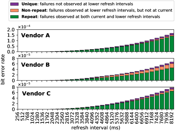
Observation 1: A large proportion of cells that are observed to fail at a given refresh interval are likely to fail again at a higher refresh interval.
Corollary 1: Determining the set of failing cells at a given refresh interval provides a large proportion of the failures found at lower refresh intervals.
4.3.3 Variable Retention Time Effects
We observe variable retention time (VRT) effects that prevent reliable detection of failing cells. Figure 4.2 shows the number of failing cells discovered over six days of data collection using brute-force profiling at a refresh interval of 2048ms at 45∘C ambient temperature. The data is shown for a single representative chip from Vendor B, but we find a similar trend across all chips from all vendors. Profiling follows the procedure described in Algorithm 1, using six data patterns and their inverses (Section 3.2) per iteration over 800 iterations throughout the length of the test. The cumulative set of discovered failures is shown in orange and the set of failures discovered each iteration is broken up into unique (i.e., newly-discovered) failures and repeat failures, shown in purple and green, respectively.
We find that after about 10 hours of testing, brute-force profiling enters the steady-state accumulation phase, in which new failures continue to accumulate with a rate of approximately one cell every 20 seconds. In other words, it takes about 10 hours to find the base set of failures for a given refresh interval using the brute-force approach. We attribute the continual discovery of new failures to the VRT phenomenon, which can cause a cell to shift from a retention time greater than 2048ms to one that is lower. However, we also observe that the total set of failures (unique + repeat) found in each iteration is nearly constant in size, implying that the rate of failure accumulation is very close to the rate of failures leaving the failing set. This finding is consistent with prior work on DDR3 chips [369, 480], showing that newer DRAM generations face similar profiling difficulties to older generations.
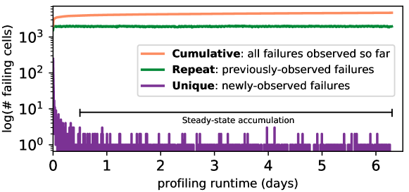
We conduct this same analysis for different refresh intervals on 368 chips from across the three DRAM vendors at 45∘C. Figure 4.3 shows the steady-state new failure accumulation rates for different refresh intervals aggregated across all chips of each vendor. The y-axis represents the steady-state new failure accumulation rate, and the x-axis shows the refresh interval. Each data point is drawn at the average value across all chips from the vendor with error bars representing the respective standard deviation. We find that the steady-state failure accumulation rate grows at a polynomial rate with respect to the refresh interval. Figure 4.3 overlays the data with well-fitting polynomial regressions of the form , and the exact fit equations are provided in the figure itself.
Observation 2: No matter how comprehensive the set of failures discovered is, the population of failing cells continues to change due to VRT effects.
Corollary 2: The retention failure profile inevitably needs to be re-generated after some period of time. In other words, online profiling is required.
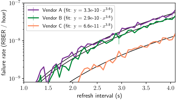
4.3.4 Data Pattern Dependence Effects
Figure 4.4 shows the cumulative number of retention failures discovered over 800 iterations spanning 6 days of continuous brute-force profiling with different data patterns across the three vendors at 45∘C. Profiling uses Algorithm 1, in which each iteration consists of writing a data pattern to DRAM, pausing refresh for 2048ms, and then checking for retention failures. New failures found by each data pattern each iteration are added to a running set representing the total number of failures discovered so far. The ratio of failures discovered by each data pattern to the total number of failures discovered by all data patterns together is plotted against time. We see that failures continue to accumulate over time, as expected from Section 4.3.3, and different data patterns uncover different fractions of failures. Of the six data patterns tested, the random pattern (solid dark purple) discovers the most failing cells across all three vendors. Observation 3: Unlike DDR3 DRAM [369], the random data pattern most closely approaches full coverage after 800 iterations spanning 6 days, but it still cannot detect every failure on its own.
Corollary 3: A robust profiling mechanism should use multiple data patterns to attain a high coverage of the set of failing cells.
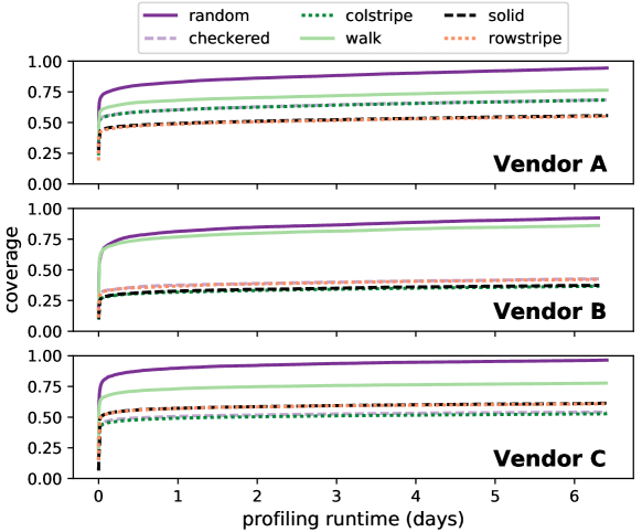
4.3.5 Individual Cell Failure Probability
We experimentally study the retention characteristics of individual DRAM cells. We find that each cell’s probability of retention failure follows a normal distribution with respect to the refresh interval. Figure 4.5(a) shows the effect of changing the refresh interval (shown normalized from between 64ms and 4096ms to s) on the probability of retention failure for almost all of the failing cells from a representative DRAM chip of Vendor B.111Cells exhibiting VRT behavior (2% of all cells for these conditions) are excluded from this plot, for ease of explanation. Each curve represents the failure cumulative distribution function (CDF) of a single cell, with failure probabilities of 0.0 and 1.0 representing 0% and 100% incorrect reads out of 16 total test iterations, respectively. All distributions’ means are normalized to s in order to highlight the similarity in failure pattern between different cells. We see that due to the normally-distributed failure probability of each cell, every cell becomes more likely to fail at longer refresh intervals.
Figure 4.5(b) shows a histogram of the standard deviations of each cell’s unique failure distribution. We find that the standard deviations follow a tight lognormal distribution, with the majority of cells having a standard deviation of less than 200ms at these conditions.222Note that this is not the same result as the well-known lognormal distribution of the number of retention failures with respect to refresh interval [191, 362]. Our observation is that the spread of each individual cell failure distribution is lognormally-distributed as opposed to the overall number of failing cells at different refresh intervals. This means that slightly extending the refresh interval results in significantly increasing the failure probability of almost all cells, which makes cells with low failure probabilities easier to detect.
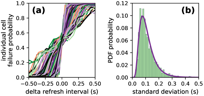
We can explain the shape of these distributions using circuit-level DRAM characteristics. As described in Section 2.1, the DRAM cell read process requires sense amplifiers to resolve the direction of a shift in bitline voltage. This shift is known as the sense amplifier voltage offset, and due to various manufacturing variations, the magnitude of this shift across different cells is found to be normally distributed [362, 593]. While using an extended refresh interval, DRAM cell leakage causes some cells’ voltage offsets to be too small to resolve correctly, causing the sense amplifier to probabilistically read an incorrect value. Therefore, our observation of normally-distributed failure probabilities for all cells (Figure 4.6(a)) is a direct consequence of the normal distribution of the sense amplifier voltage offsets. Furthermore, Li et al. [362] find that leakage components in DRAM cells follow lognormal distributions, which we hypothesize is responsible for our observation of lognormally-distributed standard deviations (Figure 4.6(b)). Given that different cells leak at lognormally-distributed rates, we would expect the length of time that a cell’s charge is within the noise margin of the sense amplifier to also be lognormally distributed.
We extend this analysis to different temperatures, and we aggregate the normal distribution fit parameters (, ) for each failing cell into the distributions shown in Figure 4.6 (a) and (b), respectively. We see that at higher temperatures, the distributions for both the means and standard deviations shift left. This means that on average, cell retention times shift to lower values and their failure distribution becomes narrower around that retention time. We can take advantage of this observation by profiling not only at a longer refresh interval, but also at a higher temperature, thus ensuring that a large majority of the cells observed to inconsistently fail at the target refresh interval and temperature are very likely to fail at the (longer) profiling refresh interval and the (higher) profiling temperature.
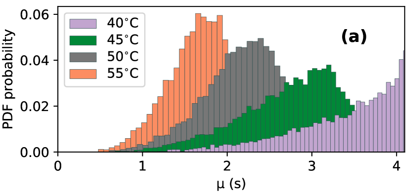
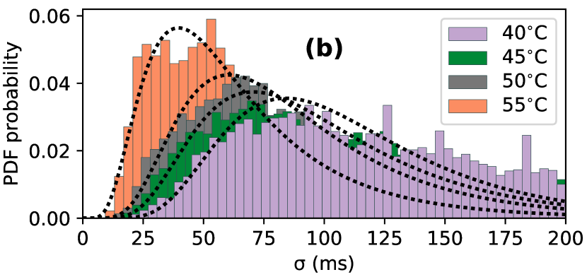
Observation 4: Cells that inconsistently fail at the target conditions may be missed with brute-force profiling, but are more likely to be found when profiling at a longer refresh interval and/or a higher temperature.
Corollary 4: In order to find failures quickly and consistently, we should profile at a longer refresh interval or a higher temperature.
By combining the normal distributions of individual cell failures from a representative chip of Vendor B, we obtain the data in Figure 4.7, which shows the failure probability for the combined distribution over different temperatures and refresh intervals. The dashed regions represent the combined standard deviation for each tested temperature, and the solid black curve in-between represents the combined mean. From this data, we draw two major conclusions: 1) at a higher temperature or a longer refresh interval, the typical cell is more likely to fail, and 2) raising the temperature and extending the refresh interval have similar effects on cell failure probability (e.g., at 45∘C, a 1s change in refresh interval has a similar effect to a 10∘C change in temperature).
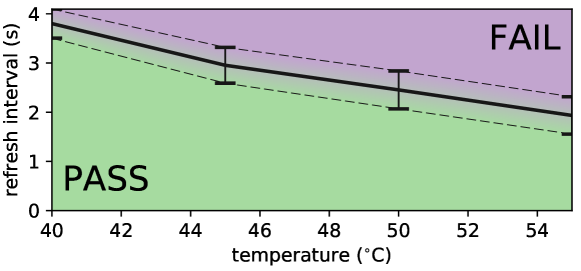
4.4 Reach Profiling
Reach profiling accelerates the process of finding the set of DRAM cells that experience retention failures by profiling DRAM under conditions that increase the likelihood of failure, called reach conditions. This enables the profiler to discover the failures much more quickly, leading to a significant reduction in overall profiling runtime. Given a set of desired target conditions consisting of a target refresh interval and a target operating temperature, the key idea of reach profiling is to profile at reach conditions, a combination of a longer refresh interval and a higher temperature relative to the target conditions. As experimentally demonstrated in Section 4.3.5, each DRAM cell is more likely to fail at such reach conditions than at the target conditions. While this enables reach profiling to attain high failure coverage (i.e., the ratio of correctly identified failing cells over the total number of failing cells at the target conditions), it also causes reach profiling to have false positives (i.e., failing cells at the reach conditions that do not fail at the target conditions), leading to more work for a retention failure mitigation mechanism that is used to correct the retention failures (including false positives). More work done by the mitigation mechanism leads to higher overhead in terms of performance, energy, or area. This results in a complex tradeoff space between the choice of reach conditions and the resulting profiling coverage, false positive rate, and runtime.
Given this complex tradeoff space, we need to address three key questions to develop an effective implementation of reach profiling:
-
1.
What are the desirable reach conditions?
-
2.
Given the continuous accumulation of new failures (e.g., due to VRT), how long does a retention failure profile remain useful (i.e., how often must we reprofile)?
-
3.
What information does the profiler need in order to determine desirable reach conditions for a given system?
We explore the answers to these questions in the rest of this section. Then, in Section 4.5, we use our exploration to develop REAPER, a robust implementation of reach profiling.
4.4.1 Desirable Reach Conditions
The three key metrics of profiling, coverage, false positive rate, and runtime (Section 4.1.2), lead to contradictory optimization goals. While an ideal configuration would achieve high coverage, low false positive rate, and low runtime, we find that there is a large tradeoff space involving these three goals. Using experimental data, we demonstrate the large scale of the tradeoff space inherent in reach profiling and show the effects of changing the refresh interval and the temperature on the three key profiling metrics. We present data for interesting choices of reach conditions and analyze the results to show how the profiling system can make a reasonable choice.
Manipulating Refresh Interval and Temperature
Figure 4.8 demonstrates the effect of choosing different reach profiling conditions on failure coverage and false positive rate for a representative chip. In order to perform this analysis, brute-force profiling is conducted at regularly spaced points throughout the graphs in Figure 4.8 using 16 iterations of 6 different data patterns and their inverses as per Algorithm 1. Each point in the graph space is then treated as a target condition with all other points as its reach conditions. This results in a distribution of coverage/false positive rates for every delta temperature/refresh interval combination.
We find that these distributions are highly similar for each delta temperature/refresh interval combination, with standard deviations of less than 10% of the data range for both coverage and false positive rate. This allows us to use the means of these distributions to reasonably demonstrate the overall effect of manipulating the temperature and/or refresh interval independently of a particular target refresh interval. We show these means in Figure 4.8, with effectively representing any target refresh interval and all other points in the figure representing its reach conditions. The contours represent the coverage (top graph) and false positive rate (bottom graph).333The contours are not perfectly smooth due to variations in the data resulting from small shifts (0.25∘C) in temperature throughout testing and the probabilistic nature of retention failures, including VRT effects. As these two graphs show, by increasing the refresh interval and/or temperature, we can obtain a higher failure coverage (Figure 4.8, top), as expected given the individual cell failure probability analysis in Section 4.3.5. However, this also results in an increase in the false positive rate (Figure 4.8, bottom). Thus, there is a direct tradeoff between coverage and false positive rate.
Profiling runtime is more difficult to evaluate since it depends on the profiling refresh interval, number of profiling iterations (see Algorithm 1), and overheads of reading and writing the data patterns to all of DRAM. We experimentally find that the amount of time taken to read/write data to all DRAM channels and check for errors is slightly less than 250ms for our evaluated chips. So, we assume a fixed overhead of 250ms per profiling iteration per data pattern tested. Figure 4.9 shows the results of such an analysis for a representative chip where represents profiling at the target conditions (i.e., brute-force profiling) and all other points show the results of reach profiling with the same analysis as in Figure 4.8. Here, each contour curve shows the profiling runtime at different reach conditions, all normalized to the runtime at the target refresh interval (i.e., brute-force profiling runtime). Profiling runtime is determined by the number of profiling iterations required to achieve over 90% coverage.
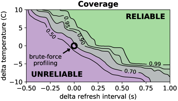
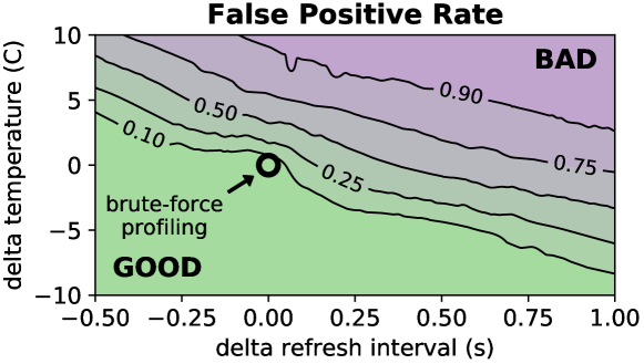
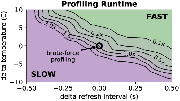
We see that we can obtain drastic profiling runtime speedups by aggressively increasing the reach conditions (e.g., +0.5s, +5∘C), but from Figure 4.8, we know that this will result in a very high number of false positives (e.g., over 90% false positive rate). Although the runtime numbers in Figure 4.9 assume a fixed coverage, we observe the same trends across different coverage requirements. Therefore, we conclude that high coverage and low runtime are generally competing goals to low false positive rates, and choosing a good set of reach conditions at which to profile depends on the user’s and the system’s requirements and failure mitigation capabilities.
We repeat this analysis for all 368 of our DRAM chips and find that each chip demonstrates the same trends, showing that the same tradeoff analysis we have done for Figures 4.8 and 4.9 also applies to every other chip we tested. In the following section, we analyze the data presented here and determine how to select a desirable set of reach conditions.
Choice of Desirable Parameters
The exact choice of reach conditions depends on the overall system design and its particular optimization goals. For example, in a highly latency-sensitive system, the primary goal may be to minimize profiling runtime, in which case giving up a low false positive rate to obtain a low profiling runtime may be necessary. On the other hand, if the retention failure mitigation mechanism in use is intolerant to high false positive rates (e.g., discarding all DRAM rows containing failing cells), a low false positive rate may be the primary design goal. In general, the system designer should take these factors into account and make the best tradeoff for the target system.
However, although the exact choice of reach conditions depends on the system goals, we observe from Figures 4.8 and 4.9 that higher coverage and higher runtime are directly and positively correlated, and both come at the expense of false positives. This means that when selecting suitable reach profiling conditions, the system designer can feasibly select as high a refresh interval/temperature as possible that keeps the resulting amount of false positives tractable. This approach primarily relies on identifying the cost of false positives for the particular system in question, possibly sacrificing the ability to handle a large number of false positives in favor of low profiling runtime.
As a concrete example, from studying data similar to those presented in Figures 4.8 and 4.9 averaged across all 368 chips, we find that for 99% coverage at a modest 50% false positive rate, we attain a profiling runtime speedup of 2.5x over the brute-force mechanism when we extend the refresh interval by 250ms. We find that we can push the speedup to over 3.5x while maintaining the same level of coverage by either increasing the temperature or lengthening the refresh interval even further, but such aggressive reach profiling conditions result in greater than 75% false positive rates.
4.4.2 Online Profiling Frequency
In order to enable a longer refresh interval, we not only have to provide a way to profile for retention failures, but also have to guarantee that retention failure profiling provides sufficient coverage to prevent erroneous system operation. Given failures that are missed by profiling due to less-than-100% coverage and non-zero new failure accumulation rates (Section 4.3.3), we need a method by which to estimate profile longevity, i.e., the amount of time before a profile is no longer correct (i.e., when reprofiling becomes necessary). In this section, we analyze the types of errors that can be missed by profiling and present a theoretical model for allowable error rates and profile longevity.
Failures Missed by Profiling
Retention failure profiling can only capture cells that fail at the profiling conditions. Cells missed during profiling due to DPD effects (Section 4.3.4) and newly-failing cells that did not fail during profiling due to environmental factors (e.g., temperature shifts, soft errors) or due to VRT effects (Section 4.3.3) cannot be observed by profiling. Prior works acknowledge that there will inevitably be failures that are missed by profiling and argue that some form of ECC is necessary to allow safe operation with a longer refresh interval [369, 282, 480]. Our observation of continuously-accumulating new failures in LPDDR4 DRAM chips (Section 4.3) leads us to agree with this argument for the use of ECC. Thus, in order to enable online profiling, we need to determine 1) what error rates can be tolerated by an ECC-based system and 2) at what point the accumulated failures will exceed the correction capability of ECC and require reprofiling.
Allowable Errors and Tolerable Error Rates
In order to estimate the probability of system failure given DRAM retention errors in the presence of various types of error correction codes (ECC), we estimate the error rate as observed by the system, called the uncorrectable bit error rate (UBER), as a function of the raw bit error rate (RBER), defined as the ratio of failing DRAM cells. We define system failure as exceeding an UBER of 1) for consumer applications [400] and 2) for enterprise applications [501].
Given a general system using -bit ECC (with defined as no ECC, as SECDED ECC [381], etc.) and an ECC word size of , we define the UBER as the probability of observing an error in a single DRAM ECC word, normalized to the number of bits per ECC word:
| (4.2) |
We obtain an uncorrectable error in an ECC word when we have an -bit error . This means that we can expand Equation 4.2 in terms of :
| (4.3) |
representing the sum of the probabilities of all possible -bit ECC uncorrectable errors. In particular, for and , we have 0 and 8 additional bits per 64-bit data word, respectively. For these cases, Equation 4.3 takes the form:
| (4.4) | ||||
The probability of an -bit error in a -bit word can be modeled by a binomial distribution, assuming that DRAM retention failures are independent and randomly distributed, as has been shown in previous work [37, 571]. Given that these assumptions hold, we can use the RBER as the probability of a single-bit failure within DRAM, and expand the probability of an -bit failure in a -bit ECC word using a binomial distribution in terms of :
| (4.5) |
Putting the pieces together, we arrive at:
| (4.6) |
Table 4.1 summarizes the maximum tolerable RBER for a target UBER of , for various choices of ECC strength. In order to provide comparison points, the table also translates the tolerable RBER into actual number of tolerable bit errors for various DRAM sizes.
| ECC Strength | ||||
|---|---|---|---|---|
| No ECC | SECDED | ECC-2 | ||
| Tolerable RBER | ||||
| 512MB | ||||
| 1GB | ||||
| 2GB | ||||
| 4GB | ||||
|
# Tolerable Bit Errors |
8GB | |||
Thus, for any target UBER, we can compute the tolerable RBER, and hence the maximum number of cells that can be allowed to escape (i.e., not be detected by) our retention failure profiling mechanism while still maintaining correct DRAM operation. By applying the maximum tolerable RBER to the RBER at any desired target refresh interval, we can directly compute the minimum coverage required from a profiling mechanism in order for the retention failure mitigation mechanism to guarantee correct system operation.
Profile Longevity
Given the maximum tolerable number of retention failures provided by Table 4.1, the number of failures missed by profiling due to imperfect profiling coverage, and the accumulation rate of new failures as measured in Section 4.3.3, we can estimate , the length of time before we need to reprofile, as:
| (4.7) |
For example, with a 2GB DRAM and SECDED ECC as the failure mitigation mechanism, we can afford up to failures while still maintaining correct DRAM operation. Assuming an aggressive target refresh interval of 1024ms at 45∘C, we empirically observe 2464 retention failures (Figure 4.1) and a new failure accumulation rate of cells / hour (Figure 4.3). With 99% coverage, we compute cells, and applying Equation 4.7, we obtain days. We can use a similar analysis to determine the profile longevity for any desired configuration and choose an appropriate tradeoff point between the different reach profiling parameters.
4.4.3 Enabling Reliable Relaxed-Refresh Operation
In order to determine good reach conditions at which to profile for a real system running at a longer refresh interval than the default, we need to know two key pieces of information: 1) the particular retention failure mitigation mechanism in use, so that we can constrain the reach profiling tradeoff space, and 2) detailed chip characterization data, in order to make reliable estimates of reach profiling benefits and profile longevity, allowing us to determine which point in the tradeoff space will provide the best overall system performance/energy improvement.
The choice of retention failure mitigation mechanism determines the hardware/energy/performance overhead of managing failing cells, which determines how aggressively we can push the target/reach conditions before the system can no longer cope with the number of failures and false positives. The mitigation mechanism therefore constrains both the target conditions (i.e., the resultant RBER without mitigation) and the maximum number of false positives, which in turn restricts the range of the reach conditions.
Detailed chip characterization data (as in Figures 4.8 and 4.9) is necessary to produce accurate estimates of all of the parameters of the actual system, including the expected RBER, the profile longevity, the required coverage, and even the reach conditions themselves. While these parameters can be estimated from general trends across many chips, the variations among different chips mean that truly reliable relaxed refresh operation requires estimating profiling parameters based on data from the actual chip.
Currently, DRAM vendors do not provide this data, but it would be reasonable for vendors to provide this data in the on-DIMM serial presence detect (SPD) as done in [315]. Otherwise, the user would have to characterize his/her own device. Even though a detailed characterization may take prohibitive amounts of time, a few sample points around the tradeoff space could provide enough information in conjunction with the general trends across many devices to develop accurate estimations. However, the general problem of efficiently obtaining per-chip characterization data is itself an open research direction and is beyond the scope of this work. Once these two critical pieces of information are available, the system designer can decide what the best tradeoff is between profile longevity, coverage, false positive rate, and runtime according to his/her own system configuration. Despite the overall trend similarities we observe between the DRAM chips we evaluate in Section 4.3, the optimal choice of reach conditions depends on the particular system and its tradeoffs between cost, performance, power, and complexity, and it is up to the user to determine the most suitable configuration for his/her own needs.
4.5 REAPER: Example End-to-End Implementation
Reach profiling provides a general-purpose retention failure profiling methodology whose exact use and design parameters (Section 4.4.3) depend on the error mitigation mechanism used for reduced-refresh-rate operation. A system designer should utilize reach profiling uniquely depending on desired performance/energy targets and ease/overhead of implementation. For example, the designer is free to choose where to implement the core profiling algorithm (e.g., at the memory controller, the operating system, etc.), how to save and restore the state of DRAM before and after a profiling round (i.e., each individual instance of online profiling consisting of all iterations and data patterns), how to efficiently profile large portions of DRAM without significant performance loss, etc. However, a thorough exploration of the design space regarding the implementation of reach profiling is beyond the scope of this paper.
In order to effectively present the insight behind the tradeoffs involved in reach profiling, we provide and evaluate REAPER, a naïve (yet robust) example implementation of reach profiling that assumes a full-system pause each time retention failures are profiled. REAPER enables a variety of retention failure mitigation mechanisms [370, 449, 582, 571, 366, 434] for reliable operation at longer refresh intervals. We experimentally validate that, even with these worst-case assumptions, reach profiling preserves a significant amount of the benefit of an ideal profiling mechanism that has zero overhead while outperforming brute-force profiling in terms of both performance and power consumption.
4.5.1 REAPER Implementation
Reach profiling requires the ability to manipulate the DRAM refresh interval and/or the DRAM temperature, both of which can be achieved with commodity off-the-shelf DRAM. REAPER implements reach profiling in firmware running directly in the memory controller. Each time the set of retention failures must be updated, profiling is initiated by gaining exclusive access to DRAM. REAPER has the ability to manipulate the refresh interval directly, but for simplicity, we assume that temperature is not adjustable (as shown in Section 4.3.5, manipulating either the temperature or the refresh interval achieves the same effect). REAPER conducts reach profiling and stores the addresses of the failing cells it finds at locations dictated by the retention failure mitigation mechanism of choice.444Profiling involves modifying the contents of DRAM. Data must be saved and restored before and after profiling is run, respectively. While a naïve implementation may flush all DRAM data to secondary storage (e.g., hard disk drive, SSD, NVM) or other parts of DRAM, a more efficient implementation could hide most or all of this latency. Efficiently implementing DRAM data save and restore is an orthogonal problem to this work. Therefore, we do not take DRAM data save and restore overheads into account in our performance and energy evaluations. At the completion of profiling, REAPER releases exclusive DRAM access and the system resumes normal operation. In the remainder of this section, we describe how this implementation of reach profiling can be combined with two example retention failure mitigation mechanisms from prior work to reduce refresh operations.
REAPER Supporting ArchShield
As a demonstrative example, we combine REAPER with ArchShield [434] to enable refresh rate reduction. ArchShield requires a small amount of additional logic in the memory controller for detecting accesses to known-faulty addresses, which are stored in 4% of DRAM in a reserved segment known as the FaultMap. The REAPER firmware provides these faulty addresses via periodically profiling DRAM for retention failures following the methodology in Section 3.2. All detected failures are stored into the FaultMap, which ArchShield accesses to determine which failing addresses must be remapped.
REAPER Supporting Multi-Rate Refresh
In order to show REAPER’s flexibility for integration with other retention failure mitigation mechanisms, we describe REAPER working with RAIDR [370]. RAIDR groups DRAM rows into different bins, according to the rows’ retention times, and applies different refresh rates to each bin. REAPER enables RAIDR by periodically updating the Bloom filters using the set of failures discovered each time profiling is conducted. This enables the system to reduce the refresh interval for most of the rows within DRAM, which results in overall system performance increase and energy reduction.
4.5.2 Evaluation Methodology
Given that profiling rounds require on the order of seconds or minutes (Section 4.5.3) and the time between online profiling rounds can be on the order of hours (Section 4.4.2), we cannot feasibly simulate workloads in order to demonstrate latency effects due to online profiling. Instead, we simulate our workloads without the profiling overhead and report performance results using throughput in terms of instructions-per-cycle (IPC). We then use the following model to compute overall system performance accounting for online profiling overhead:
| (4.8) |
where is the measured throughput of simulated workloads, and is the proportion of real system time spent in profiling. Our profiling overhead model assumes worst-case configurations, pessimistically assuming that applications make zero forward progress while profiling. Our full system performance model roughly estimates the worst-case performance degradation expected from an implementation of reach profiling.
We use Ramulator [316, 6] to evaluate performance and DRAMPower [3] to evaluate DRAM power consumption. We simulate 20 multiprogrammed heterogeneous workload mixes, each of which is constructed by randomly selecting 4 benchmarks from the SPEC CPU2006 benchmark suite [7]. Multi-core system performance is measured in terms of the weighted speedup metric [535, 145]. We provide our evaluated system configuration in Table 4.2.
| Processor | 4 cores, 4GHz clock frequency, 3-wide issue, 8 MSHRs/core, 128-entry instruction window |
|---|---|
| Last-level Cache | 64B cache line, 16-way, 8MB cache size |
| Memory Controller | 64-entry read/write request queues, FR-FCFS scheduling policy [493, 634], open/closed row policy [314, 313] for single/multi-core |
| DRAM | LPDDR4-3200 [250], 4 channels, 1 rank, 8 banks/rank, 32K-256k rows/bank, 2KB row buffer |
4.5.3 Performance and Energy Evaluation
We develop a detailed model for profiling overhead, taking into account extra DRAM accesses required for profiling, latencies involved in reading/writing data patterns to DRAM, and time consumed waiting for the extended refresh intervals. We use this model in conjunction with Equation 4.8 to reliably estimate worst-case system performance impact and additional DRAM power consumption. In this section, we present our 1) model for profiling performance and power consumption overhead for brute-force profiling and reach profiling, and 2) results for end-to-end system performance and DRAM power consumption using brute-force profiling, reach profiling, and the ideal profiling mechanism that does not impact system performance or power consumption. We find that while profiling power consumption overheads are very low across a wide range of DRAM sizes and refresh intervals, profiling performance overheads become significant for large DRAM chips and high online profiling frequencies. In such cases where profiling performance significantly impacts overall system performance, reach profiling maintains a large fraction of the benefits of using a longer refresh interval (e.g., providing 14.8% higher performance than brute-force profiling on average for a 64Gb chip running at a 1280ms refresh interval at 45∘C), as we show in Section 4.5.3.
Profiling Overhead
We model the overhead of online profiling by accumulating the latencies of individual operations required to run a single round of profiling. We assume that profiling requires a full system pause, with no useful work being done while the profiler is running. One round of profiling consists of iterations, each of which consists of reading/writing DRAM with different data patterns. Our end-to-end runtime model is as follows:
| (4.9) |
where is the profiling refresh interval that DRAM must wait with refresh disabled in order to accumulate errors; is the time to write a data pattern into DRAM; and is the time to read DRAM and compare against the original data pattern. For 32 8Gb DRAM chips with 1024ms, 0.125s222This value is based on empirical measurements from our infrastructure using 2GB of LPDDR4 DRAM. We scale this number according to DRAM size throughout our evaluation to account for the larger number of accesses., 6, and 6, we find that 3.01 minutes, and for 32 64Gb chips, 19.8 minutes.
In order to demonstrate the overall system performance degradation from profiling, Figure 4.10 plots the proportion of overall system time spent profiling for a variety of different profiling intervals and DRAM sizes assuming 16 iterations of brute-force profiling at 1024ms using 6 data patterns and their inverses. The x-axis represents the online profiling frequency in hours, and the y-axis shows the proportion of total system-time spent profiling. To compare the brute-force method against REAPER, we plot the performance overheads with hashed (brute-force) and solid (REAPER) bars. We show results for the 2.5x profiling runtime speedup of reach profiling over brute-force profiling, found experimentally in Section 4.4.1. The differently-colored bars represent DRAM modules consisting of 32 individual DRAM chips, with each chip ranging from 8Gb to 64Gb in size. We observe that at shorter profiling intervals, the performance degradation is prohibitively high and is exacerbated by larger DRAM chip sizes. For example, we find that for a profiling interval of 4 hours and a 64Gb chip size, 22.7% of total system time is spent profiling with brute-force profiling while 9.1% of time is spent profiling with REAPER.
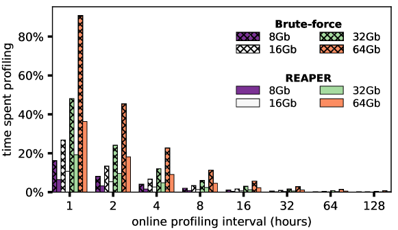
In order to demonstrate the overall DRAM power overhead associated with profiling, Figure 4.11 shows the total DRAM power required for profiling across the same sweep of configurations as Figure 4.10. Power consumption overhead is calculated using the average energy-per-bit costs for different DDR commands obtained from our LPDDR4 DRAMPower model [3]. We estimate the number of extra commands required for profiling and show the total DRAM energy consumed for one round of profiling divided by the online profiling interval. The x-axis represents the online profiling frequency in hours, and the y-axis shows the DRAM power consumption in nanowatts. We see that power consumption has a strong dependence on DRAM size and shows a similar scaling trend as profiling performance overhead with respect to the profiling interval. However, the absolute power consumption is very low (on the order of nanowatts), because the majority of profiling runtime is spent waiting for retention failures to occur (i.e., the profiling refresh interval) rather than actively accessing DRAM. We show in Section 4.5.3 how profiling itself results in negligible additional power in the DRAM system, even in the extreme case of very frequent profiling and large DRAM sizes.
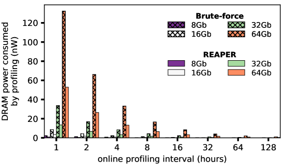
.
End-to-end System Evaluation Results
We evaluate the overall effects of REAPER on system performance and DRAM power consumption by applying our profiling overhead model to Equation 4.8. We compare REAPER with both online brute-force profiling and the ideal profiling mechanism that incurs no performance or energy overhead. The ideal mechanism mirrors the approach taken by prior works on refresh rate reduction [370, 449, 582, 571, 366, 434], which assume that offline profiling is sufficient. Considerable evidence against the sufficiency of offline profiling is provided by both prior work on DRAM characterization [369, 282] and our own observations (Sections 4.3.3 and 4.4.2). We exclude ECC-scrubbing based mechanisms from our evaluations due to their passive approach to failure profiling, which cannot guarantee failure coverage in the same way as an active profiling mechanism, as discussed in Section 3.2.
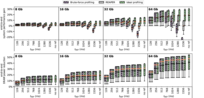
Figure 4.12 shows the results of this analysis, demonstrating the overall system performance improvement (top) and DRAM power consumption reduction (bottom) due to operating with a longer refresh interval across all of our simulated workloads for a variety of DRAM sizes each consisting of 32 individual DRAM chips of the specified capacity (8-64Gb). Each triplet of boxes presents results for online brute-force profiling, REAPER, and the ideal profiling mechanism, in order from left to right. Results are shown for various lengthened refresh intervals from 128ms to 1536ms and for the case of no refresh, which is shown as a single box. For each refresh interval, the profiling parameters used to compute overhead are obtained using the experimental data for failure rates at 45∘C as shown in Section 4.3. Profile longevity is estimated in the best case for each configuration, assuming that the profilers achieve full coverage each time they are run. This assumption is reasonable for profilers achieving high (e.g., 99%) coverage and allows us to decouple the results from failure rates of specific DRAM chips. Results are all normalized to the base performance or power consumption at the default refresh interval of 64ms without profiling. The boxes represent the distribution of benchmarks from the 25th to the 75th percentiles, the whiskers show the data range, and the orange and black lines represent medians and means, respectively. We make four major observations based on these results.
First, REAPER enables a high performance improvement and a high DRAM power reduction by reliably increasing the refresh interval. REAPER enables 512ms as the best overall operating point across all evaluated DRAM chip sizes, providing an average of 16.3% (maximum 27.0%) performance improvement and an average of 36.4% (maximum 47.4%) power reduction for 64Gb chips. This is very close to the average performance gain of 18.8% (31.2% maximum) and average power reduction of 41.3% (54.1% maximum) that comes with eliminating all refreshes (rightmost “no ref” bars).
Second, REAPER significantly outperforms the brute-force mechanism, especially at high refresh intervals ( 1024ms). While the ideal profiling mechanism enables increasing gains with longer refresh intervals, both REAPER and brute-force profiling overheads become more significant for refresh intervals beyond 1024ms. This is due to the high VRT failure accumulation rate (Section 4.3.3) at long refresh intervals, which requires a high online profiling frequency. However, at such high refresh intervals, REAPER preserves much more of the ideal profiling benefit than does brute-force profiling. For example, with 64Gb DRAM chips, at a refresh interval of 1024ms, using REAPER provides 13.5% average (24.7%) maximum performance improvement while using brute-force profiling provides only 7.5% average (18% maximum) performance improvement. REAPER’s performance benefit over brute-force profiling increases with longer refresh intervals because REAPER can sustain higher online profiling frequencies better, showing that REAPER is superior to brute-force profiling. For refresh intervals below 512ms, both REAPER and brute-force profiling provide benefits that are very close to that of ideal profiling since the performance overhead of both mechanisms is low. This is due to the low VRT failure accumulation rate observed in Section 4.3.3 for short refresh intervals, resulting in a high profile longevity. However, short refresh intervals do not provide the full benefits of employing longer refresh intervals, so we would like to enable as high a refresh interval as possible with as low overhead as possible.
Third, REAPER enables high performance operation at very long refresh intervals that were previously unreasonable to operate the system at. For refresh intervals longer than 512ms, the high online profiling frequency means that profiling overhead becomes significant (as supported by Figure 4.10), and this overhead eventually results in overall performance degradation. At a refresh interval of 1280ms, the performance impact of profiling becomes clearly visible: using brute-force profiling leads to overall system performance degradation (-5.4% on average). However, REAPER still maintains significant performance benefit (8.6% on average) at 1280ms, demonstrating that REAPER enables longer refresh intervals that were previously unreasonable to operate the system at.
Fourth, both REAPER and brute-force profiling have negligible impact on overall DRAM power consumption across all refresh intervals and DRAM chip sizes. While Figure 4.11 shows that REAPER consumes significantly less power than brute-force profiling at the same configuration, profiling power consumption is a very small fraction of total DRAM power consumption to begin with. This means that although the profiling process has a large effect on overall system performance, it does not contribute significantly to DRAM power consumption. Thus, both REAPER and brute-force profiling are effective at greatly reducing DRAM power consumption by enabling a longer refresh interval.
We can use the results of Figure 4.12 to estimate the benefits obtained by using any retention failure mitigation mechanism. For example, ArchShield [434] extends the default refresh interval up to 1024ms at the cost of approximately 1% overall system performance (Section 5.1 of [434]). The overall system performance improvement can be estimated by subtracting ArchShield’s reported performance cost (in [434]) from the ideal profiling performance gain (in Figure 4.12), resulting in an overall performance improvement of 15.7% on average (28.2% maximum) using 64Gb DRAM chips at a refresh interval of 1024ms. However, as we show the need for an online profiling mechanism (Section 4.4.2), the actual overall performance benefit must be adjusted to account for profiling overhead. We observe performance improvements of 6.5% on average (17% maximum) when ArchShield is combined with brute-force profiling, and 12.5% on average (23.7% maximum) when it is combined with REAPER. Thus, we find that using REAPER leads to an average performance improvement of 5.6% over using brute-force profiling. A similar analysis can be conducted using other state-of-the-art retention failure mitigation mechanisms to estimate overall system speedup and DRAM power consumption.
We conclude that REAPER is an effective and low-overhead profiling mechanism that enables high-performance operation at very long refresh intervals (beyond 1024ms) that were previously not reasonable to employ due to the high associated profiling overhead. As a caveat to the data presented in this section, it is important to note that Figures 4.10, 4.11, and 4.12 are all based on specific assumptions (e.g., 45∘C temperature, 2.5x performance improvement of reach profiling vs. online brute-force profiling, 32 chips per DRAM module, 100% coverage by profiling, 20 randomly-formed heterogeneous workload mixes) and we are not covering the entire design space with these results. This means that there likely exist other conditions under which REAPER may perform even better, including both different temperatures, at which we would expect failure rates and therefore profile longevity to change, and varying system requirements (e.g., choice of retention failure mitigation mechanism, target profiling coverage and false positive rate, target profile longevity, target UBER, etc.). These conditions may result in different choices of reach profiling parameters, which can lead to a higher-than-2.5x performance improvement for reach profiling over brute-force profiling. This increase in reach profiling performance translates directly to reduction in profiling overhead, which in turn translates to even greater end-to-end system performance improvement and greater DRAM power reduction than presented here.
4.6 Summary
In this chapter, we rigorously explore the complex tradeoff space associated with DRAM retention profiling mechanisms using new experimental data from 368 modern LPDDR4 DRAM chips. In an effort to develop a rigorous understanding of how retention failure profiling can be made viable for increasing the refresh interval, we experimentally characterize DRAM chips at various temperatures and refresh intervals and analyze the probability of failure of different cells in DRAM as well as tradeoffs of retention time profiling. Following rigorous analysis of the collected data, we propose reach profiling, a technique whose key idea is to profile DRAM at a longer refresh interval and/or a higher temperature relative to the target refresh interval/temperature in order to quickly discover an overwhelming majority of all possible failing cells at the target conditions. We show that reach profiling enables significant system performance improvement and DRAM power reduction, outperforming the brute-force approach and enabling high-performance operation at longer refresh intervals that were previously unreasonable to employ due to the high associated profiling overhead. We conclude that reach profiling can be an enabler for many past and future DRAM refresh reduction mechanisms. We also hope that the new experimental characterization and the analysis of the data retention characteristics of modern LPDDR4 DRAM devices presented herein will serve as an enabler for others to develop new techniques to tackle the difficult yet critical problem of DRAM refresh.
?chaptername? 5 Understanding and Modeling DRAM On-Die ECC
In the previous chapter, we present out experimental study of DRAM data-retention error characteristics in DRAM chips without on-die ECC. In this chapter, we extend such studies to DRAM chips with on-die ECC. Our goal in this chapter is to understand the relationship between pre- and post-correction errors in a way that enables us to understand overcome the barrier that on-die ECC poses for understanding DRAM pre-correction error characteristics.
5.1 Background and Motivation
DRAM has long since been a crucial component in computing systems primarily due to its low cost-per-bit relative to alternative memory technologies [347, 420, 434, 429]. However, while subsequent technology generations have substantially increased overall DRAM capacity, they have not achieved comparable improvements in performance, energy efficiency, and reliability [91, 429, 347, 197]. This has made DRAM a significant performance and energy bottleneck in modern systems [420, 429].
To address this challenge, researchers propose a wide variety of solutions based on insights and understanding about DRAM behavior gleaned from system-level DRAM error characterization studies [37, 89, 91, 94, 138, 164, 199, 201, 220, 268, 269, 267, 280, 282, 284, 283, 305, 312, 295, 296, 294, 343, 346, 370, 369, 371, 397, 449, 459, 460, 468, 480, 485, 505, 510, 541, 540, 545, 550, 551, 553, 559, 558, 571, 580, 590, 602]. These studies deliberately induce errors in a DRAM device by experimentally testing the device at conditions that exacerbate physical DRAM error mechanisms (e.g., charge leakage, circuit interference). The resulting errors directly reflect the effects of the error mechanisms, providing researchers with insight into the physical properties that underlie DRAM operation (e.g., data-retention, circuit timings, data-pattern sensitivity). Researchers can then exploit these insights to develop new mechanisms that improve DRAM and overall system efficiency.
Unfortunately, continued DRAM technology scaling heralds grave reliability concerns going forward primarily due to increasing single-bit error rates that reduce manufacturing yield [347, 434, 435, 405, 276, 211, 183, 397, 541, 540, 381, 510]. While manufacturers traditionally use redundant circuit elements (e.g., rows, columns) to repair manufacturing faults [434, 538, 276, 212, 384, 183], mitigating growing single-cell error rates is no longer tractable using circuit-level redundancy alone [405].
To maintain desired yield targets, DRAM manufacturers have recently supplemented circuit-level redundancy with on-die error correction codes (on-die ECC)111Also known as in-DRAM ECC and integrated ECC. [434, 435, 405, 276, 448]. On-die ECC is completely invisible to the system [276, 435]: its implementation, encoding/decoding algorithms, and metadata are all fully contained within the DRAM device and provide no feedback about error detection and/or correction to the rest of the system. On-die ECC is independent of any particular DRAM standard, and JEDEC specifications do not constrain how the on-die ECC mechanism may be designed [250]. Since DRAM manufacturers primarily employ on-die ECC to transparently improve yield, they do not publicly release the ECC implementation details. Therefore, on-die ECC is typically not described in DRAM device datasheets, and neither publications [276, 270, 448, 330, 331, 109] nor whitepapers [405, 229] provide details of the ECC mechanism for a given product.
5.1.1 Motivation: On-Die ECC’s Impact on Studies
Unfortunately, on-die ECC has dire implications for DRAM error characterization studies since it censors the true errors that result from physical error mechanisms inherent to DRAM technology. For a device with on-die ECC, we observe only post-correction errors, which do not manifest until pre-correction error rates exceed the ECC’s correction capability. However, the way in which the ECC mechanism transforms a specific uncorrectable error pattern is implementation-defined based on the mechanism’s design, which is undocumented, proprietary, opaque, and possibly unique per product. Thus, on-die ECC effectively obfuscates the pre-correction errors such that they cannot be measured simply by studying post-correction errors without knowing the ECC scheme.
Figure 5.1 demonstrates the differences in the observed data-retention bit error rate (BER) (y-axis) for different on-die ECC schemes (explained in Section LABEL:subsec:ecc_bg) given the same pre-correction BER (x-axis). We generate this data in simulation using EINSim, which is described in detail in Section 5.3. We see that the observed error rates are dependent on the particular ECC scheme used, and without knowledge of which ECC scheme is used in a given device, there is no easy way to tie the observed error rates to the pre-correction error rates.
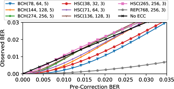
This means that post-correction errors may not follow expected, well-studied distributions based on physical error mechanisms (e.g., exponential temperature dependence of charge leakage rates [191, 369, 35], lognormal retention-time distributions [191, 362, 370, 468]) but rather device-architecture-specific shapes that cannot be reliably compared with those from a device with a different ECC scheme. We discuss and experimentally demonstrate the implications of this observation in Sections 6.2 and 5.6, respectively.
5.1.2 Overview of Error Inference (EIN)
Thus, on-die ECC effectively precludes studying DRAM error mechanisms, motivating the need for a DRAM error characterization methodology that isolates the effects of intrinsic DRAM behavior from those of the ECC mechanism used in a particular device. To this end, our goal in this work is to overcome the barrier that on-die ECC presents against understanding DRAM behavior in modern devices with on-die ECC. To achieve this goal, we develop Error-correction INference (EIN), a statistical inference methodology that uses maximum a posteriori (MAP) estimation to 1) reverse-engineer the ECC scheme and 2) infer the pre-correction error rates from only the observed post-correction errors. We follow a methodical four-step process:
First, we tackle the unique reverse-engineering problem of determining the on-die ECC scheme without any visibility into the error-correction algorithm, the redundant data, or the locations of pre-correction errors. Our approach is based on the key idea that even though ECC obfuscates the exact locations of the pre-correction errors, we can leverage known statistical properties of pre-correction error distributions (e.g., uniform-randomness [526, 37, 468, 295]) in order to disambiguate the effects of different ECC schemes (Section 5.2).
We develop statistical models to represent how a given pre-correction error distribution will be transformed by an arbitrary ECC scheme (Section 5.2.1). Our models are parameterized by i) the desired ECC scheme and ii) statistical properties of the pre-correction error distribution. We then formulate the reverse-engineering problem as a maximum a posteriori (MAP) estimation of the most likely model given experimental data from real devices (Section 5.2.4).
Second, in order to compute several expressions in our statistical models that are difficult to evaluate analytically, we develop EINSim[4], a flexible open-source simulator that numerically estimates the error-detection, -correction, and -miscorrection effects of arbitrary ECC schemes for different pre-correction error distributions (Section 5.3). EINSim models the lifetime of a given ECC dataword through the encoding, error injection, and decoding processes faithful to how these steps would occur in a real device (Section 5.3.1). To ensure that EINSim is applicable to a wide range of DRAM devices and standards, we design EINSim to be modular and easily extensible to additional error mechanisms and distributions. Third, we perform the first experimental study of DRAM devices with on-die ECC in open literature and demonstrate how EIN infers both: i) the on-die ECC scheme and ii) the pre-correction error rates. We study the data-retention characteristics of 232 (82) state-of-the-art LPDDR4 DRAM devices with (without) on-die ECC from one (three) major DRAM manufacturers across a wide variety of temperatures, refresh rates, and test patterns. To accurately model pre-correction errors in EINSim, we first reverse-engineer:
-
•
The layout and dimensions of internal DRAM cell arrays.
-
•
The locations and frequency distribution of redundant DRAM rows used for post-manufacturing repair.
Applying EIN to data from devices with on-die ECC, we:
-
•
Find that the on-die ECC scheme is a single-error correction Hamming code [193] with ( = 136, = 128, = 3).
-
•
Show that EIN can infer pre-correction error rates given only post-correction errors.
Fourth, we demonstrate EIN’s usefulness by providing a proof-of-concept experimental characterization study of the data-retention error rates for the DRAM devices with on-die ECC. We test across different refresh intervals and temperatures to show that EIN effectively enables inferring the pre-correction error rates, which, unlike the ECC-obfuscated post-correction error rates, follow known shapes that result from well-studied device-independent error mechanisms.
5.1.3 Applicability of EIN
EIN allows researchers to more holistically study the reliability characteristics of DRAM devices with on-die ECC by exposing the pre-correction error rates beneath the observed post-correction errors. This enables researchers to propose new ideas based on a more general understanding of DRAM devices. To demonstrate how EIN may be useful, we provide: 1) several examples of studies and mechanisms that EIN enables and 2) a discussion about the implications of continued technology scaling for future error characterization studies.
5.1.4 Example Applications
We provide several examples of potential studies and mechanisms that are enabled by knowing pre-correction error rates, which on-die ECC masks and EIN reveals:
-
•
Runtime Error Rate Optimization: A mechanism that intelligently adjusts operating timings/voltage/frequency to meet dynamically changing system performance/energy/reliability targets (e.g., Voltron [94], AL-DRAM [343], AVA-DRAM [344], DIVA-DRAM [346]) typically needs to profile the error characteristics of a device for runtime decision-making. If the particular ECC scheme is known (e.g., using EIN), such a mechanism can leverage device-independent DRAM error models for decision-making and quickly interpolating or extrapolating “safe” operating points rather than having to: (1) use complex, likely non-parametric, device-specific models for each supported ECC scheme or (2) characterize each device across its entire region of operation.
-
•
Device Comparison Studies: EIN enables fair comparisons of DRAM error characteristics between devices with different (and without) on-die ECC mechanisms. This is useful for studying the evolution of error characteristics over time, which provides insight into the state of the industry and future technology trends. With DRAM error rates continuing to worsen (discussed in Section 5.1.5), such studies can help predict how much worse future devices may be and how well current/future error-mitigation mechanisms will cope.
-
•
Reverse-Engineering Other ECCs: As we discuss in Section 5.3.6, EIN is applicable to other systems (e.g., rank-level ECC, Flash memory) whose ECC schemes are typically also proprietary. Reverse-engineering their ECC schemes can be useful for various reasons [117, 74, 157, 596, 115], including failure analysis, security evaluation, forensic analysis, patent infringement, and competitive analysis. For these systems, EIN may provide a way to reverse-engineer the ECC scheme without requiring hardware intrusion or internal access to the ECC mechanism as typically required by previous approaches [568, 569, 596, 115] (discussed in Section 3.1.1).
We hope that future work will use EIN well beyond these use cases and will develop new characterization-driven understanding of devices with on-die ECC.
5.1.5 Applicability to Future Devices
Despite its energy and reliability benefits, on-die ECC does not fundamentally prevent error rates from increasing. Therefore, future DRAM devices may require stronger error-mitigation solutions, further obfuscating pre-correction error rates and making error characterization studies even more difficult.
Similarly, other memory technologies (e.g., Flash [78, 74], STT-MRAM [233, 630, 328], PCM [481, 339, 340, 598, 512], Racetrack [619], RRAM [597]) suffer from ongoing reliability concerns, and characterizing their error mechanisms requires surmounting any error-mitigation techniques they use. EIN takes a first step towards enabling a holistic understanding of devices whose error characteristics are not directly visible, and we hope that future work leverages this opportunity to develop new mechanisms to tackle the reliability challenges that lie ahead.
5.2 Statistically Modeling DRAM and ECC
We begin by formalizing the relationship between pre- and post-correction error distributions and expressing reverse-engineering as a maximum a posteriori (MAP) estimation problem. Our approach is grounded on the key idea that pre-correction errors arise from physical error mechanisms with known statistical properties, and because different ECC schemes transform these distributions in different ways, we can use what we know about both the pre- and post-correction error distributions to disambiguate different ECC schemes. This section provides a step-by-step derivation of EIN, the statistical inference methodology we propose in this work.
5.2.1 Statistically Modeling Error Correction Codes
Consider an ECC mechanism implementing an binary block code as illustrated in Figure 5.2. The ECC encoding algorithm transforms a dataword out of the set of all possible datawords into a valid codeword out of the set of all possible valid codewords . Likewise, the decoding algorithm transforms a codeword (potentially invalid due to errors) out of the set of all possible codewords into a corrected dataword out of the set of all possible corrected datawords .
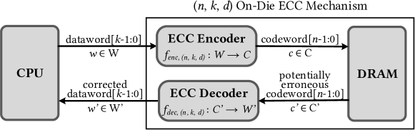
can be thought of as a deterministic mapping222While non-deterministic encoding/decoding algorithms exist, they are typically not used with the simple ECCs found in DRAM. If more complex ECCs must be considered (e.g., LDPC [116, 74]), our models can be extended to treat the encoding/decoding functions as probabilistic transformations themselves. from the finite set of inputs to a finite set of outputs :
| (5.1) |
This means that for a particular ECC scheme , the probability of observing output is determined by the probabilities that its corresponding inputs occur:
| (5.2) |
From this perspective, if we know both 1) the ECC scheme and 2) the frequency distribution of all possible input values , we can calculate the corresponding distribution of all possible output values.333Note that since ECC decoding is generally not injective (i.e., multiple codewords may map to a single decoded dataword), we cannot determine exactly which input produced an observed output. Inverting this relationship, if we experimentally measure the frequency distribution of output values from a real device, we can determine the probability of having made such observations given 1) a suspected ECC scheme and 2) an expected frequency distribution of all possible inputs. Section 5.2.3 describes what we know about pre-correction error distributions and how we leverage this knowledge to disambiguate different suspected ECC schemes.
5.2.2 Experimental Observables
Solving Equation 5.2 requires measuring the relative frequency distribution of post-correction datawords (i.e., ). For example, if we use 64-bit datawords, we have unique datawords. Unfortunately, a single DRAM device has on the order of millions of datawords, which is nowhere near enough to obtain a representative sample of the full distribution.
Instead, we divide into subsets, , which each comprise all possible datawords with errors. Using this approach, a relative frequency distribution of the contains only categories, and even a single DRAM device contains more than enough samples to obtain a representative distribution. Experimentally, measuring the number of errors in each dataword simply requires counting errors.444There is no fundamental reason for this choice beyond experimental convenience; if another choice is made, our analysis still holds but will need to be modified to accommodate the new choice of . We can then rewrite Equation 5.2 in terms of the subsets :
| (5.3) |
Unfortunately, this approach requires knowing the exact layout of ECC words in memory. This may be difficult since multiple bits are read/written together at the granularity of a burst (Section 2.1.1), and each burst may contain one or more ECC words with an arbitrary bit-to-ECC-word mapping.
To circumvent this problem, we instead consider the probability of observing errors per burst, where each burst comprises dataword(s) from one or more ECC schemes. Mathematically, the total number of errors in a burst is the sum of the individual per-dataword error counts and is computed by convolving the per-dataword error-count distributions. Counting errors at burst-granularity is independent of the layout of ECC words within a burst assuming that ECC words are contained within burst boundaries so that bursts can be read/written independently. However, if a different design is suspected, even longer words (e.g., multiple bursts) may be used as necessary.
5.2.3 Statistically Modeling DRAM Errors
To estimate the relative frequencies of the pre-correction codewords , we exploit the fact that errors arise from physical phenomena that follow well-behaved statistical distributions. Throughout this work, we focus on data-retention error distributions since they are well-studied and are easily reproduced in experiment. However, EIN is applicable to any experimentally-reproducible error distribution whose statistical properties are well-understood (e.g., reduced activation-latency [91, 346, 294, 343, 295, 296], reduced precharge-latency [91, 551, 550], reduced voltage [94], RowHammer [312, 422, 426]).
As described in Section 2.2.5, data-retention errors occur when a charged cell capacitor leaks enough charge to lose its stored value. This represents a “1” to “0” error for a charged true-cell (i.e., programmed with data “1”), and vice-versa for an anti-cell [369, 312, 115]. Due to random manufacturing-time variations [134, 626, 362, 305, 343, 344, 312], certain cells are more prone to data-retention errors than others [369, 571, 191, 370, 276, 305]. Furthermore, absolute data-retention error rates depend on operating conditions such as refresh timings, data patterns, ambient temperature, and supply voltage. Through extensive error characterization studies, prior works find that, for a fixed set of testing conditions (e.g., , temperature), data-retention errors show no discernible spatial patterns [191, 370, 37, 571, 526] and can be realistically modeled as uniform-randomly distributed [295, 526, 37] independent events [526].
To model an arbitrary pre-correction error distribution in our analysis, we introduce an abstract model parameter that encapsulates all state necessary to describe the distribution. In general, is a set of two key types of parameters: i) experimental testing parameters (e.g., data pattern, timing parameters, temperature) and ii) device microarchitectural characteristics (e.g., spatial layout of true- and anti-cells). We incorporate into our analysis as a dependency to the terms in Equation 5.3:
| (5.4) |
Ideally, all of the parameters that comprise are known at testing time. Unfortunately, experiments are often imperfect, and internal device characteristics are difficult to obtain without proprietary knowledge or laborious reverse-engineering. If such parameters are unknown, we can infer them alongside the unknown ECC scheme.555While we could lump the unknown ECC scheme into as an unknown microarchitectural characteristic, we keep it logically separate since represents what we already understand about DRAM devices, and the unknown ECC scheme represents what we do not.
In this work, we model data-retention errors as uniform-random, independent events among cells programmed to the “charged” state with a fixed probability determined by testing conditions. then encapsulates i) the single-bit error probability, called the raw bit error rate (RBER), ii) the programmed data pattern, and iii) the spatial layout of true-/anti-cells.
Unfortunately, evaluating Equation 5.4 analytically is difficult even for data-retention errors due to the complexity of the interactions between the ECC scheme and the parameters encompassed by . Instead, we numerically estimate the solution to Equation 5.4 using Monte-Carlo simulation as described in Section 5.3. This approach allows our analysis to flexibly take into account arbitrarily complex model parameters (e.g., detailed microarchitectural characteristics, nontrivial error models).
5.2.4 Inferring the Model Parameters
We now formulate the reverse-engineering task as a maximum a posteriori (MAP) estimation problem over a set of hand-selected ECC schemes that are either directly mentioned in context with on-die ECC (HSC(71, 64, 3) [229, 236, 435] and HSC(136, 128, 3) [270, 405, 330, 331, 109]) or are used as demonstrative examples of applying our methodology to devices with stronger and/or more complicated codes (e.g., BCH(, , ), HSC(, , ), REP(3, 1, 3)). Note that we also take into account implementation details of each of these schemes (e.g., systematic vs. non-systematic encodings) using our simulation infrastructure as we describe in Section 5.3.3. To reverse-engineer the unknown ECC scheme , we start by expressing it as the most likely ECC scheme out of all possible schemes given a set of observations :
| (5.5) |
Unfortunately, we cannot directly evaluate Equation 5.5 since our observations are measured from a device with a fixed ECC scheme. Instead, we use the Bayes theorem to express Equation 5.5 in terms of the probability of obtaining measurements given an arbitrary ECC scheme , which we can calculate using the relationship in Equation 5.3. This yields:
| (5.6) |
Note that we ignore the denominator (i.e., the marginal likelihood) in Equation 5.6 because it is a fixed scale factor independent of and does not affect the maximization result.
We assume a uniformly-distributed prior (i.e., ) given that we cannot guarantee anything about the on-die ECC implementation. By restricting our analysis to only the aforementioned ECC schemes, we already exclude any schemes that we consider to be unrealistic. In principle, we could assign greater or lower probability mass to schemes that have been mentioned in prior work or that are exceedingly expensive, respectively, but we choose not to do so because i) we cannot guarantee that the devices we test are similar to those mentioned in prior work, and ii) we want to demonstrate the power of our methodology without biasing the results towards any particular ECC schemes. The likelihood function (i.e., ) incorporates the experimental data we obtain from real devices. As we show in Section 5.2.2, our measurements provide us with the probability of observing an -bit error in each of independent DRAM bursts. Defining as a random variable representing the number of erroneous bits observed in a single burst and assuming observations are independent events (validated in Section 5.2.3), we rewrite the likelihood function as:
| (5.7) |
This is essentially a multinomial probability mass function (PMF) evaluated at , where each probability mass is computed using Equation 5.4. Unfortunately, as described in Section 5.2.3, the model parameter encapsulates the pre-correction error rate, which we do not know and cannot measure post-correction. Therefore, for each ECC scheme , we first maximize the likelihood distribution over :
| (5.8) |
Inserting the result of Equation 5.8 into our original optimization objective (Equation 5.6), we obtain the final objective function to optimize in order to reverse-engineer the ECC scheme used in our devices:
| (5.9) |
where the inner product term is calculated using Equation 5.4.
After the ECC scheme is reverse-engineered, we can repeatedly apply Equation 5.8 to solve for across many different experiments (i.e., observations). Since represents all parameters necessary to describe the pre-correction error distribution (described in Section 5.2.3), this is equivalent to reverse-engineering the pre-correction error rate. With the ECC scheme known as , Equation 5.8 simplifies to:
| (5.10) |
With Equations 5.9 and 5.10, we can reverse-engineer both i) the ECC scheme and ii) the pre-correction error rates from observed post-correction errors for any DRAM device whose error distributions are obscured by ECC. In Section 5.5.3, we experimentally demonstrate how to apply Equation 5.9 to real devices with on-die ECC.
5.3 Simulation Methodology
To apply EIN to data from real devices, we develop and publicly release EINSim [4], a flexible open-source C++-based simulator that models the life of a dataword through the entire ECC encoding/decoding process. EINSim accounts for different ECC implementations and pre-correction error characteristics to ensure that EIN is applicable to a wide variety of DRAM devices and standards. This section describes EINSim’s extensible design and explains how EINSim can be used to solve the optimization problems formulated in Section 5.2.
5.3.1 EINSim High-Level Architecture
Figure 5.3 shows a high-level diagram of the logical flow of data through EINSim’s different components. To model a DRAM experiment, we simulate many individual burst-length accesses that each access a different group of cells. Each burst simulates an experimental measurement, yielding a distribution of measured values across all simulated bursts. We describe the function of each simulator component.
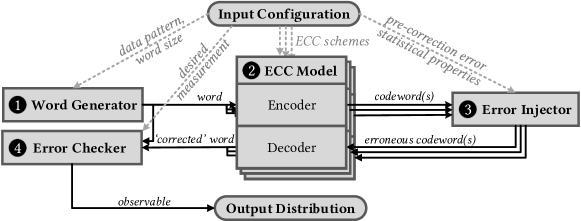
Word generator constructs a bitvector using commonly tested data patterns (e.g., 0xFF, 0xAA, RANDOM) [12, 369, 282, 283, 589, 346, 468], simulating the data written to DRAM.
ECC model encompasses an ECC implementation, including the encoding/decoding algorithms and implementation details such as systematic vs. non-systematic encodings. Because a single word from the word generator may comprise multiple ECC datawords, EINSim provides a configurable mapping for decomposing the word into ECC datawords.
Error injector injects errors into a given codeword according to a configurable error distribution. We implement support for data-retention errors as described in Section 5.2.3. We provide configurable parameters for the spatial distribution of true-/anti-cells (e.g., alternating per row) and the single-bit probability of failure (i.e., RBER). Errors are injected uniform-randomly across each bit that can fail (i.e., each “charged” cell per the chosen true-/anti-cell layout and data pattern) using a Bernoulli distribution with equal to the desired RBER normalized by the ratio of all cells that can fail, which ensures that the simulated error rate meets the target RBER on average.
Error checker takes the pre- and post-correction words as inputs and calculates a user-defined measurement (e.g., total number of bit-flips). This corresponds to an experimental observable as explained in Section 5.2.2.
5.3.2 EINSim Validation
We validate EINSim using a combination of manual and automatic unit tests. For the ECC model, we 1) provide tests for detecting/correcting the right amount of errors (exhaustively/sample-based for short/long codes); 2) hand-verify the inputs/outputs of encoders/decoders where reasonable; 3) hand-validate the generator/parity-check matrices and/or code generator polynomials against tables of known values (e.g., [112]); and 4) validate the minimum distance and weight distributions of codewords. Due to the simplicity of how we model the true-/anti-cell layout and data-retention errors, we validate the error-injection correctness by 1) manual inspection and 2) using summary statistics (e.g., distribution of errors across many simulated bursts).
5.3.3 Applying EINSim to Experimental Data
To analyze data taken from a real experiment, we configure the simulation parameters to match the experiment and simulate enough read accesses (e.g., >) to allow the distribution of simulated measurements to numerically estimate the real experimental measurements. This approach effectively solves Equation 5.4 through Monte-Carlo simulation for any model parameters {, } that can be simulated using EINSim. Figure 5.1 in Section 5.1.1 provides several examples of evaluating Equation 5.4 across a wide range of model parameters {, } using a 256-bit input word programmed with a RANDOM data pattern. The X-axis shows the pre-correction bit error rate (BER), i.e., the RBER component of , and the Y-axis shows the observed BER, which is computed by taking an expectation value over the distribution resulting from solving Equation 5.4. Curves represent different ECC schemes , and each data point represents one simulation of words, subdividing each word into multiple ECC datawords as necessary.
We see that each ECC scheme transforms the pre-correction error rate differently. For example, stronger codes (e.g., REP(768, 256, 3), BCH(78, 64, 5)) dramatically decrease the observed BER, whereas weaker codes (e.g., HSC(265, 256, 3)) have a relatively small effect. Interestingly, we see that many of the codes actually exacerbate the error rate at high enough pre-correction error rates because, on average, the decoder mistakenly “corrects” bits without errors more often than not. These examples demonstrate that different ECC schemes have different effects on the pre-correction error distribution, and Equation 5.9 exploits these differences to disambiguate schemes.
5.3.4 Inferring the Model Parameters
To infer the model parameters and , which represent the ECC scheme and pre-correction error distribution characteristics, respectively, we need to perform the optimization given by Equation 5.9. We do this using a grid search across and , simulating uniformly-spaced error rates for each of several different ECC schemes, data patterns and true-/anti-cell layouts. While a denser grid may improve precision, this configuration sufficiently differentiates the models we analyze (Section 5.5.3).
The solutions to Equation 5.9 are the inferred ECC scheme and pre-correction error distribution characteristics that best explain the experimental observations. From there, we can use Equation 5.10 evaluated with the known ECC scheme in order to determine for any additional experiments that we run (e.g., different error rates).
5.3.5 Inference Accuracy
MAP estimation rigorously selects between known models and inherently can neither confirm nor deny whether the MAP estimate is the “real” answer. We identify this as a limitation of EIN in Section 5.3.8. However, in the event that a device uses a scheme that is not considered in the MAP estimation, it would be evident when testing across different experimental conditions and error rates since it is unlikely that any of the chosen ECC schemes would be the single maximum-a-posteriori scheme (i.e., best explaining the observed data) across all experiments.
We can also use confidence intervals to gauge the error in each MAP estimate. This requires repeating the MAP estimation over bootstrap samples [142] taken from the observed data . The min/max or 5th/95th percentiles are typically taken to be the confidence bounds.
5.3.6 Applying EIN to Other Systems
EIN can be extended to any ECC-protected communication channel provided that we can induce uncorrectable errors whose pre-correction spatial distribution follows some known property (e.g., uniform-randomness). Examples include, but are not limited to, DRAM rank-level (i.e., DRAM-controller-level) ECC and other memory technologies (e.g., SRAM, Flash, Phase-Change Memory).
5.3.7 Applying EIN to Data from Prior Studies
EIN is applicable to data presented in a prior study if the study supplies enough information to solve Equation 5.10. This requires that the study provides both: 1) the pre-correction error characteristics, either directly as statistical distributions or implicitly through the experimental methodology (e.g., device model number, tested data patterns) and 2) the distribution of errors amongst post-correction words as discussed in Section 5.2.2. If these are known, EIN can infer both the ECC scheme and the pre-correction error rates from the given data.
5.3.8 Limitations of EIN
EIN has three main limitations. However, in practice, these limitations do not hurt its usability since both DRAM and ECC design are mature and well-studied topics. We discuss each limitation individually:
- 1.
-
2.
Requires knowledge and control of errors. Using EIN requires i) knowing statistical properties of the spatial distribution of pre-correction errors, and ii) the ability to induce uncorrectable errors. Fortunately, EIN can use any one of the many well-studied, easily-manipulated error mechanisms that are fundamental to DRAM technology (e.g., data retention, RowHammer, reduced-latency access; see Section 5.2.3). Such mechanisms are unlikely to change dramatically for future devices (e.g., retention errors are modeled similarly across decades of DRAM technologies [190, 207, 364, 191, 411, 588, 323, 106]), which means that EIN will likely continue to be applicable.
-
3.
Cannot identify bit-exact error locations. While EIN infers pre-correction error rates, it cannot determine the bit-exact locations of pre-correction errors. Unfortunately, since multiple erroneous codewords may map to each visible dataword, we are not aware of a way to infer error locations without insight into the exact ECC implementation (e.g., algorithms, redundant data). However, inferring error rates is sufficient to study aggregate distributions, and we leave error localization to future work.
5.4 Experimental Methodology
We experimentally characterize 232 LPDDR4 [250] DRAM devices with on-die ECC from a single major DRAM manufacturer that we cannot disclose for confidentiality reasons. For comparison purposes, we test 82 LPDDR4 DRAM devices of the previous technology generation without on-die ECC from across three major DRAM manufacturers. Given that DRAM manufacturers provide neither: i) non-ECC counterparts of devices with on-die ECC nor ii) a mechanism by which to disable on-die ECC, the older-generation devices provide our closest point of comparison. We perform all testing using a home-grown infrastructure that provides precise control over DRAM timing parameters, bus commands, and bus addresses. Our infrastructure provides reliable ambient temperature control between 40∘C - 55∘C with a tolerance of of C. To improve local temperature stability for each DRAM device throughout testing, a local heating source maintains DRAM at 15∘C above the ambient temperature at all times, providing an effective DRAM temperature testing range of 55∘C - 70∘C.
5.5 Experimentally Inferring On-Die ECC and Pre-Correction Error Rates Using EIN
In this section, we apply EIN to infer the i) on-die ECC scheme and ii) pre-correction error rates of real devices with on-die ECC. Before doing so, we validate our uniform-random statistical model for pre-correction errors and determine the layout of true-/anti-cells to accurately model the pre-correction error distribution of the devices that we test.
5.5.1 Validating Uniform-Random Retention Errors
Our model for data-retention errors (Section 5.2.3) treats errors as independent, uniform-randomly distributed events based on observations made in several prior works [191, 370, 37, 571, 526, 295]. For such errors, the total number of errors in each fixed-length -bit region of DRAM follows a binomial distribution [468, 37, 571] parameterized by the RBER :
| (5.11) |
Before demonstrating the use of EIN, we first validate that the independent, uniform-random data-retention error model holds for the devices that we test by comparing experimentally-measured error distributions to the expected distributions. Figure 5.4 shows both the expected and experimental probabilities of observing an -bit error in a single 256-bit word throughout DRAM at fixed operating conditions of and 60∘C for a single representative DRAM device without on-die ECC.
The experimental data is well predicted by the binomial distribution and diverges only at extreme error counts that have few experimental samples. This validates modeling retention errors using a uniform-random distribution for the devices without on-die ECC. We repeat this experiment across all of our devices without on-die ECC for various word sizes, refresh windows, and temperatures, and we find that the uniform-random model holds across all experiments.
5.5.2 Determining the True-/Anti-Cell Layout
We reverse-engineer the true-/anti-cell layout in the devices with on-die ECC to ensure that we can accurately model the pre-correction error distribution in simulation (as described in Section 5.3.1, we only inject errors in cells programmed to the “charged” state). We do this by studying the locations of data-retention errors after disabling refresh for a long time (e.g., >30 minutes), which causes most cells to leak to their discharged state.666A small number of cells do not follow the overall pattern due to either i) extraordinarily long retention times or ii) ECC correction. Figure 5.5 illustrates the resulting pattern, showing how individual rows comprise entirely true- or anti-cells, and contiguous groups of either 824 or 400 rows alternate throughout a bank. In simulation, we model each DRAM burst to be entirely composed of either true- or anti-cells with a 50% probability. This accurately models sampling an arbitrary burst from the entire memory address space.
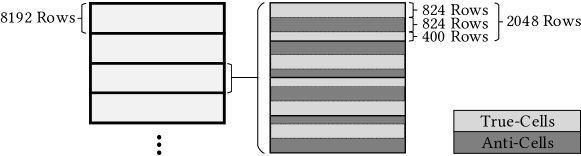
Despite the observed true-/anti-cell pattern, we find that a small amount of uniquely randomly-distributed rows in each bank do not follow the pattern shown in Figure 5.5. Instead, these rows alternate true- and anti-cells every byte and are often found in clusters of two or more. A histogram of the number of such rows, called outlier rows, per bank across all 232 devices with on-die ECC is shown in Figure 5.6 alongside a best-fit negative-binomial distribution curve. Both the shape of the frequency distribution and the observed clustering are consistent with post-manufacturing repair row remapping techniques [212]. Since these rows have a different true- and anti-cell composition, they add unwanted noise to our reverse-engineering analysis. While we could account for them in our simulations, we simply skip testing these rows in our experimental analysis to avoid unnecessary complexity.
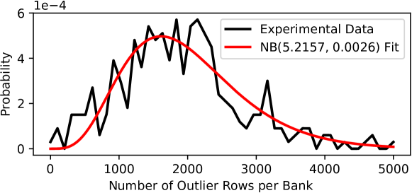
5.5.3 Applying EIN to DRAM with On-Die ECC
We demonstrate applying EIN to the DRAM devices with on-die ECC using the experimental configuration shown in Table 5.1. The error distribution resulting from a single experiment provides the PMF given by Equation 5.3, which forms the observations in the overall optimization problem (Equation 5.9).
| Model Parameter | Experiment | Simulation |
|---|---|---|
| Word Size | 256-bits | |
| True-/Anti-Cell Layout | 50%/50% at word-granularity | |
| Data Pattern | RANDOM | RANDOM and 0xFF |
| Outlier Rows | Skipped | Ignored |
| Temperature | 70∘C | Encompassed in the RBER |
| 5 minutes | Encompassed in the RBER | |
Using a representative device, we perform a single experiment at the conditions shown in Table 5.1, measuring a post-correction BER of 0.041578. Then, configuring EINSim with the parameters listed under “Simulation” in Table 5.1, we evaluate the full optimization problem of Equation 5.9 using the grid-search approach described in Section 5.3.4.
Figure 5.7 presents the negative log-likelihoods (Equation 5.8) of the eight highest-likelihood ECC schemes for each of the 0xFF and RANDOM data patterns. Models are sorted in order of increasing likelihood (i.e., decreasing negative log-likelihood) from left to right for each data pattern. Bars show black confidence intervals spanning the min/max values when bootstrapping the observed data times (described in Section 5.3.5). The confidence intervals are tight enough to appear as a single line atop each bar. Note that the 0xFF models have low likelihoods (i.e., higher bars), which agrees with the fact that our experimental data is obtained using a RANDOM data pattern.
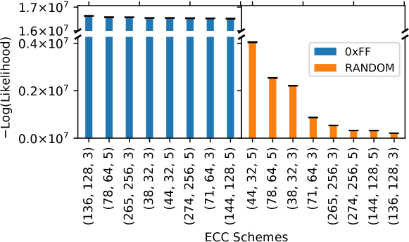
The smallest (i.e., rightmost) bar represents the most likely model, which provides the final reverse-engineered model parameters, including the ECC scheme and the pre-correction error rate. For greater insight into the results, Table 5.2 describes the five highest-likelihood models in detail.
| Log-Likelihood | ||||
|---|---|---|---|---|
| Value | Bootstrap (Min, Max) | ECC Code | RBER | Data Pattern |
| 2.12e-5 | (2.09e-5, 2.15e-5) | (136, 128, 3) | 0.038326 | RANDOM |
| 3.21e-5 | (3.18e-5, 3.24e-5) | (144, 128, 5) | 0.039113 | RANDOM |
| 3.26e-5 | (3.22e-5, 3.29e-5) | (274, 256, 5) | 0.039995 | RANDOM |
| 5.38e-5 | (5.32e-5, 5.43e-5) | (265, 256, 3) | 0.039956 | RANDOM |
| 8.74e-5 | (8.69e-5, 8.79e-5) | (71, 64, 3) | 0.038472 | RANDOM |
The data indicates that a Hamming single-error correction code with (, , ) is the most likely ECC scheme out of all models considered. This result is consistent with several industrial prior works [405, 330, 331, 109].777We obtained this result without informing the prior distribution about the existence of prior works. If instead we had done so as mentioned in Section 5.2.4, (136, 128, 3) [405, 330, 331, 109] and (71, 64, 3) [229, 236] ECC code would have been more overwhelmingly likely. Compared to most of the other codes we consider, (136, 128, 3) code has a relatively low error-correction capability (i.e., 1 bit per 136 codeword bits), which is reasonable for a first-generation on-die ECC mechanism and requires a relatively simple, low-overhead circuit implementation.
The MAP estimate of provides the most likely pre-correction error rate (i.e., RBER) and data pattern to explain the observed data. Note that on-die ECC actually increases the error rate at these testing conditions, likely due to a high incidence of miscorrections as described in Section 5.3.3. EIN correctly infers that our experiment uses the RANDOM data pattern, which is indicated by the relatively low likelihoods of the models that assume a 0xFF data pattern.
Figure 5.8 shows the full PMF of Equation 5.4 for all sixteen models considered in Figure 5.7. The maximum-a-posteriori model (dashed) and the experimental data (solid) are shown alongside all other models (dotted). When shown graphically, it is clear that EIN effectively performs a rigorous best-fit analysis over several models to the experimental observations.
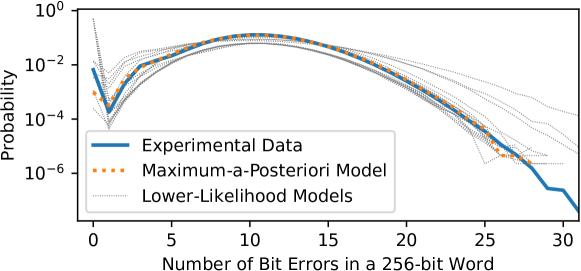
We repeat this analysis across different devices, temperatures, refresh windows, and data patterns and consistently find the (136, 128, 3) ECC code to be the maximum-a-posteriori model. Thus, we conclude that the (136, 128, 3) ECC code is the ECC scheme used in the tested devices.
We draw three key conclusions from this application of EIN.
First, EIN infers the on-die ECC scheme with no visibility into the encoded data or error-detection/-correction information, without disabling the ECC mechanism, and without tampering with the hardware in any way.
Second, EIN can simultaneously infer several components of that might not be known. While we demonstrate a simple inference over only two data patterns in addition to the pre-correction error rate, we could also infer other characteristics (e.g., true-/anti-cell composition, refresh window, temperature). In general, is extensible to any model parameter that can be implemented in simulation (i.e., in EINSim).
5.6 Data-Retention Error Characterization of DRAM Devices with On-Die ECC
Having reverse-engineered the on-die ECC scheme, we characterize data-retention error rates with respect to both and temperature to demonstrate how EIN enables studying pre-correction errors in practice. To our knowledge, this is the first work to provide a system-level error characterization study of DRAM devices with on-die ECC in open literature in an effort to understand the pre-correction error characteristics.
5.6.1 Data-Retention Error Rate vs. Refresh Window
Figure 5.9 shows the measured data-retention error rates for DRAM devices with and without on-die ECC using different values at a fixed temperature of 50∘C using a 0xFF data pattern. Each of the five distributions shows the minimum and maximum error rates observed for different groups of devices organized by manufacturer. We also show the pre-correction error rates inferred using EIN.
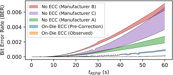
The data shows that the observed error rates for devices with on-die ECC lie far below those of devices without on-die ECC. This is consistent with observations from prior works [405, 331, 330], which find that on-die ECC is a strong enough error-mitigation mechanism to allow for refresh rate reduction. Unfortunately, the observed error rates do not provide insight into how the core DRAM technology has changed because it is unclear how much of the error margin improvement is simply a result of ECC.
EIN solves this problem. By inferring the pre-correction error rates, we observe considerable error margin for even the pre-correction error rates, implying that on-die ECC may be unnecessary at these testing conditions. This may seem surprising at first sight, since error rates are believed to be increasing with technology generation [276, 397, 405, 435]. However, on-die ECC’s goal is to combat single-cell errors at worst-case operating specifications [405] (i.e., C, ms [250], worst-case usage characteristics). Unfortunately, our testing infrastructure currently cannot achieve such conditions, and even if it could, the pathological access- and data-patterns depend on the proprietary internal circuit design known only to the manufacturer. Therefore, our observations do not contradict expectations, and we conclude that for devices with on-die ECC: i) on-die ECC effectively reduces the observed error rate and ii) both pre- and post-correction error rates are considerably lower than those of devices without on-die ECC at our testing conditions.
This example demonstrates EIN’s strengths: EIN separates the effects of a device’s particular ECC mechanism from the raw error rates of the DRAM technology and enables a meaningful comparison of error characteristics between devices with (or without) different ECC schemes. EIN enables this analysis for any error mechanism that EIN is applicable to (Section 5.3.6).
5.6.2 Data-Retention Error Rate vs. Temperature
Data-retention error rates are well-known to follow an exponential relationship with respect to temperature [191, 369, 35], and prior works [369, 292, 323] exploit this relationship to extrapolate error rates beyond experimentally feasible testing conditions. We show that on-die ECC distorts this exponential relationship such that observed error rates cannot be reliably extrapolated, and EIN recovers the underlying exponential relationship.
Figure 5.10 shows the exponential relationship for a single representative device with on-die ECC at a fixed refresh window of 10s on a semilog scale. Measurements (orange, ) are taken between the temperature limits of our infrastructure (55∘C - 70∘C, illustrated with a grey background), and the inferred pre-correction error rates (blue, ) and the hypothetical error rates if the on-die ECC scheme were a stronger double-error correction (144, 128, 5) code (green, ) are shown. We show exponential fits to data within the measurable region for all three curves. Outside of the measurable region (i.e., <55∘C and >70∘C), we use EINSim to extrapolate the two post-correction curves beyond the measurable region (dashed) based on the exponential fit for the pre-correction curve.
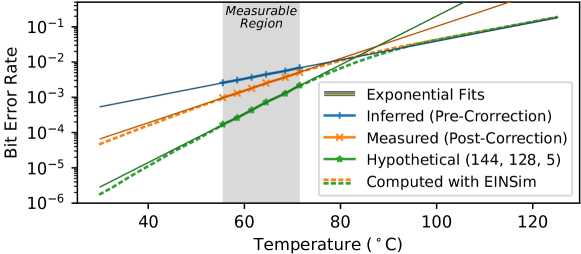
While all three curves appear to fit an exponential curve within the measurable temperature range, this is a misleading artifact of sampling only a small fraction of the overall error distribution. Across the full range, only the pre-correction curve follows the exponential relationship: both post-correction curves diverge from the exponential fit on both sides of the measurable region and follow an ECC-specific shape. This means that post-correction error rates cannot be directly fitted to an exponential curve, and extrapolating along the known exponential relationship of the data-retention error mechanism requires knowing the pre-correction error rates.
This example demonstrates how EIN recovers the statistical characteristics of the pre-correction error rates that on-die ECC obfuscates. In general, EIN enables this for any error mechanism that EIN is applicable to (discussed in Section 5.2.3), allowing future works to make use of well-studied error characteristics for devices with ECC.
5.7 Summary
We develop EIN, the first statistical inference methodology capable of determining the ECC scheme and pre-correction error rates of a DRAM device with on-die ECC. We provide EINSim [4], a flexible open-source simulator that can apply EIN across different DRAM devices and error models. We evaluate EIN with the first experimental study of 232 (82) LPDDR4 DRAM devices with (without) on-die ECC. Using EIN, we: i) find that the ECC scheme employed in the devices we test is a single-error correction Hamming code with ( = 136, = 128, = 3), ii) infer pre-correction error rates from post-correction errors, and iii) recover well-known pre-correction error distributions that on-die ECC obfuscates. With this, we demonstrate that EIN enables DRAM error characterization studies for devices with on-die ECC. We believe and hope that future work will use EIN to develop new understanding and mechanisms to tackle the DRAM scaling challenges that lie ahead.
?chaptername? 6 Understanding Exactly How On-Die ECC Obfuscates Errors
The previous chapter develops a statistical inference technique for understanding high-level properties of the on-die ECC mechanism and the pre-correction errors. This chapter takes the next step and introduces two new testing methodologies: (1) BEER, capable of identifying the exact way in which on-die ECC obfuscates errors; and (2) BEEP, capable of inferring the number and bit-exact locations of the pre-correction errors responsible for an observed post-correction error pattern.
6.1 Background and Motivation
Dynamic random access memory (DRAM) is the predominant choice for system main memory across a wide variety of computing platforms due to its favorable cost-per-bit relative to other memory technologies. DRAM manufacturers maintain a competitive advantage by improving raw storage densities across device generations. Unfortunately, these improvements largely rely on process technology scaling, which causes serious reliability issues that reduce factory yield. DRAM manufacturers traditionally mitigate yield loss using post-manufacturing repair techniques such as row/column sparing [212]. However, continued technology scaling in modern DRAM chips requires stronger error-mitigation mechanisms to remain viable because of random single-bit errors that are increasingly frequent at smaller process technology nodes [405, 276, 435, 176, 332, 397, 448, 309, 538, 369, 429, 420]. Therefore, DRAM manufacturers have begun to use on-die error correction coding (on-die ECC), which silently corrects single-bit errors entirely within the DRAM chip [405, 276, 176, 435, 467]. On-die ECC is completely invisible outside of the DRAM chip, so ECC metadata (i.e., parity-check bits, error syndromes) that is used to correct errors is hidden from the rest of the system.
Prior works [229, 435, 405, 494, 448, 330, 331, 467] indicate that existing on-die ECC codes are 64- or 128-bit single-error correction (SEC) Hamming codes [193]. However, each DRAM manufacturer considers their on-die ECC mechanism’s design and implementation to be highly proprietary and ensures not to reveal its details in any public documentation, including DRAM standards [249, 250], DRAM datasheets [237, 502, 406, 531], publications [448, 330, 331, 276], and industry whitepapers [405, 494].
6.1.1 Motivation: On-Die ECC Obfuscates Errors
Because the unknown on-die ECC function is encapsulated within the DRAM chip, it obfuscates raw bit errors (i.e., pre-correction errors)111We use the term “error” to refer to any bit-flip event, whether observed (e.g., uncorrectable bit-flips) or unobserved (e.g., corrected by ECC). in an ECC-function-specific manner. Therefore, the locations of software-visible uncorrectable errors (i.e., post-correction errors) often no longer match those of the pre-correction errors that were caused by physical DRAM error mechanisms. While this behavior appears desirable from a black-box perspective, it poses serious problems for third-party DRAM customers who study, test and validate, and/or design systems based on the reliability characteristics of the DRAM chips that they buy and use. Section 6.2.2 describes these customers and the problems they face in detail, including, but not limited to, three important groups: (1) system designers who need to ensure that supplementary error-mitigation mechanisms (e.g., rank-level ECC within the DRAM controller) are carefully designed to cooperate with the on-die ECC function [538, 435, 177], (2) large-scale industries (e.g., computing system providers such as Microsoft [149], HP [204], and Intel [228], DRAM module manufacturers [318, 533, 13]) or government entities (e.g., national labs [438, 503]) who must understand DRAM reliability characteristics when validating DRAM chips they buy and use, and (3) researchers who need full visibility into physical device characteristics to study and model DRAM reliability [190, 191, 265, 589, 141, 608, 286, 467, 297, 369, 199, 295, 294, 296, 282, 284, 283, 285, 91, 94, 468].
For each of these third parties, merely knowing or reverse-engineering the type of ECC code (e.g., -bit Hamming code) based on existing industry [448, 330, 331, 405, 494, 229] and academic [435, 467] publications is not enough to determine exactly how the ECC mechanism obfuscates specific error patterns. This is because an ECC code of a given type can have many different implementations based on how its ECC function (i.e., its parity-check matrix) is designed, and different designs lead to different reliability characteristics. For example, Figure 6.1 shows the relative probability of observing errors in different bit positions for three different ECC codes of the same type (i.e., single-error correction Hamming code with 32 data bits and 6 parity-check bits) but that use different ECC functions. We obtain this data by simulating ECC words using the EINSim simulator [467, 4] and show medians and 95% confidence intervals calculated via statistical bootstrapping [142] over 1000 samples. We simulate a 0xFF test pattern222Other patterns show similar behavior, including RANDOM data. with uniform-random pre-correction errors at a raw bit error rate of (e.g., as often seen in experimental studies [191, 276, 369, 343, 526, 94, 199, 91, 468]).
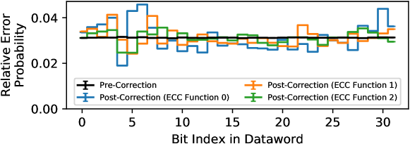
The data demonstrates that ECC codes of the same type can have vastly different post-correction error characteristics. This is because each ECC mechanism acts differently when faced with more errors than it can correct (i.e., uncorrectable errors), causing it to mistakenly perform ECC-function-specific “corrections” to bits that did not experience errors (i.e., miscorrections, which Section LABEL:subsec:ecc_bg expands upon). Therefore, a researcher or engineer who studies two DRAM chips that use the same type of ECC code but different ECC functions may find that the chips’ software-visible reliability characteristics are quite different even if the physical DRAM cells’ reliability characteristics are identical. On the other hand, if we know the full ECC function (i.e., its parity-check matrix), we can calculate exactly which pre-correction error pattern(s) result in a set of observed errors. Figure 6.1 is a result of aggregating such calculations across error patterns333Capturing approximately of the unique patterns., and Section 6.6.1 demonstrates how we can use the ECC function to infer pre-correction error counts and locations using only observed post-correction errors.
Knowing the precise transformation between pre- and post-correction errors benefits all of the aforementioned third-party use cases because it provides system designers, test engineers, and researchers with a way to isolate the error characteristics of the memory itself from the effects of a particular ECC function. Section 6.2.2 provides several example use cases and describes the benefits of knowing the ECC function in detail. While specialized, possibly intrusive methods (e.g., chip teardown [242, 561], advanced imaging techniques [209, 561]) can theoretically extract the ECC function, such techniques are typically inaccessible to or infeasible for many third-party users.
6.1.2 Mechanism: Bit-Exact ECC Recovery (BEER)
To enable third parties to reconstruct pre-correction DRAM reliability characteristics, our goal is to develop a methodology that can reliably and accurately determine the full on-die ECC function without requiring hardware tools, prerequisite knowledge about the DRAM chip or on-die ECC mechanism, or access to ECC metadata (e.g., error syndromes, parity information). To this end, we develop Bit-Exact ECC Recovery (BEER), a new methodology for determining a DRAM chip’s full on-die ECC function simply by studying the software-visible post-correction error patterns that it generates. Thus, BEER requires no hardware support, hardware intrusion, or access to internal ECC metadata (e.g., error syndromes, parity information). BEER exploits the key insight that forcing the ECC function to act upon carefully-crafted uncorrectable error patterns reveals ECC-function-specific behavior that disambiguates different ECC functions. BEER comprises three key steps: (1) deliberately inducing uncorrectable data-retention errors by pausing DRAM refresh while using carefully-crafted test patterns to control the errors’ bit-locations, which is done by leveraging data-retention errors’ intrinsic data-pattern asymmetry (discussed in Section 2.2.5), (2) enumerating the bit positions where the ECC mechanism causes miscorrections, and (3) using a SAT solver [126] to solve for the unique parity-check matrix that causes the observed set of miscorrections.
We experimentally apply BEER to 80 real LPDDR4 DRAM chips with on-die ECC from three major DRAM manufacturers to determine the chips’ on-die ECC functions. We describe the experimental steps required to apply BEER to any DRAM chip with on-die ECC and show that BEER tolerates observed experimental noise. We show that different manufacturers appear to use different on-die ECC functions while chips from the same manufacturer and model number appear to use the same on-die ECC function (Section 6.4.1). Unfortunately, our experimental studies with real DRAM chips have two limitations against further validation: (1) because the on-die ECC function is considered trade secret for each manufacturer, we are unable to obtain a groundtruth to compare BEER’s results against, even when considering non-disclosure agreements with DRAM manufacturers and (2) we are unable to publish the final ECC functions that we uncover using BEER for confidentiality reasons (discussed in Section 6.2.1).
To overcome the limitations of experimental studies with real DRAM chips, we rigorously evaluate BEER’s correctness in simulation (Section 6.5). We show that BEER correctly recovers the on-die ECC function for 115300 single-error correction Hamming codes444This irregular number arises from evaluating a different number of ECC functions for different code lengths because longer codes require exponentially more simulation time (discussed in Section 6.5.1)., which are representative of on-die ECC, with ECC word lengths ranging from 4 to 247 bits. We evaluate our BEER implementation’s runtime and memory consumption using a real system to demonstrate that BEER is practical and the SAT problem that BEER requires is realistically solvable.
To demonstrate how BEER is useful in practice, we propose and discuss several ways that third parties can leverage the ECC function that BEER reveals to more effectively design, study, and test systems that use DRAM chips with on-die ECC (Section 6.6). As a concrete example, we introduce and evaluate Bit-Exact Error Profiling (BEEP), a new DRAM data-retention error profiling methodology that reconstructs pre-correction error counts and locations purely from observed post-correction errors. Using the ECC function revealed by BEER, BEEP infers precisely which unobservable raw bit errors correspond to observed post-correction errors at a given set of testing conditions. We show that BEEP enables characterizing pre-correction errors across a wide range of ECC functions, ECC word lengths, error patterns, and error rates. We publicly release our tools as open-source software: (1) a new tool [1] for applying BEER to experimental data from real DRAM chips and (2) enhancements to EINSim [4] for evaluating BEER and BEEP in simulation.
6.2 Challenges of Unknown On-Die ECCs
This section discusses why on-die ECC is considered proprietary, how its secrecy causes difficulties for third-party consumers, and how the BEER methodology helps overcome these difficulties by identifying the full on-die ECC function.
6.2.1 Secrecy Concerning On-Die ECC
On-die ECC silently mitigates increasing single-bit errors that reduce factory yield [405, 276, 435, 176, 332, 397, 448, 309, 538, 369, 429, 420]. Because on-die ECC is invisible to the external DRAM chip interface, older DRAM standards [250, 249] place no restrictions on the on-die ECC mechanism while newer standards [253] specify only a high-level description for on-die ECC to support new (albeit limited) DDR5 features, e.g., on-die ECC scrubbing. In particular, there are no restrictions on the design or implementation of the on-die ECC function itself.
This means that knowing an on-die ECC mechanism’s details could reveal information about its manufacturer’s factory yield rates, which are highly proprietary [224, 105] due to their direct connection with business interests, potential legal concerns, and competitiveness in a USD 45+ billion DRAM market [482, 572]. Therefore, manufacturers consider their on-die ECC designs and implementations to be trade secrets that they are unwilling to disclose. In our experience, DRAM manufacturers will not reveal on-die ECC details under confidentiality agreements, even for large-scale industry board vendors for whom knowing the details stands to be mutually beneficial.555Even if such agreements were possible, industry teams and academics without major business relations with DRAM manufacturers (i.e., an overwhelming majority of the potentially interested scientists and engineers) will likely be unable to secure disclosure.
This raises two challenges for our experiments with real DRAM chips: (1) we do not have access to “groundtruth” ECC functions to validate BEER’s results against and (2) we cannot publish the final ECC functions that we determine using BEER for confidentiality reasons based on our relationships with the DRAM manufacturers. However, this does not prevent third-party consumers from applying BEER to their own devices, and we hope that our work encourages DRAM manufacturers to be more open with their designs going forward.666While full disclosure would be ideal, a more realistic scenario could be more flexible on-die ECC confidentiality agreements. As recent work [154] shows, security or protection by obscurity is likely a poor strategy in practice.
6.2.2 On-Die ECC’s Impact on Third Parties
On-die ECC alters a DRAM chip’s software-visible reliability characteristics so that they are no longer determined solely by how errors physically occur within the DRAM chip. Figure 6.1 illustrates this by showing how using different on-die ECC functions changes how the same underlying DRAM errors appear to the end user. Instead of following the pre-correction error distribution (i.e., uniform-random errors), the post-correction errors exhibit ECC-function-specific shapes that are difficult to predict without knowing precisely which ECC function is used in each case. This means that two commodity DRAM chips with different on-die ECC functions may show similar or different reliability characteristics irrespective of how the underlying DRAM technology and error mechanisms behave. Therefore, the physical error mechanisms’ behavior alone can no longer explain a DRAM chip’s post-correction error characteristics.
Unfortunately, this poses a serious problem for third-party DRAM consumers (e.g., system designers, testers, and researchers), who can no longer accurately understand a DRAM chip’s reliability characteristics by studying its software-visible errors. This lack of understanding prevents third parties from both (1) making informed design decisions, e.g., when building memory-controller based error-mitigation mechanisms to complement on-die ECC and (2) developing new ideas that rely on on leveraging predictable aspects of a DRAM chip’ reliability characteristics, e.g., physical error mechanisms that are fundamental to all DRAM technology. As error rates worsen with continued technology scaling [405, 276, 435, 176, 332, 397, 448, 309, 297, 312, 420, 429], manufacturers will likely resort to stronger codes that further distort the post-correction reliability characteristics. The remainder of this section describes three key ways in which an unknown on-die ECC function hinders third-parties, and determining the function helps mitigate the problem.
Designing High-Reliability Systems. System designers often seek to improve memory reliability beyond that which the DRAM provides alone (e.g., by including rank-level ECC within the memory controllers of server-class machines or ECC within on-chip caches). In particular, rank-level ECCs are carefully designed to mitigate common DRAM failure modes [99] (e.g., chip failure [435], burst errors [382, 129]) in order to correct as many errors as possible. However, designing for key failure modes requires knowing a DRAM chip’s reliability characteristics, including the effects of any underlying ECC function (e.g., on-die ECC) [538, 177]. For example, Son et al. [538] show that if on-die ECC suffers an uncorrectable error and mistakenly “corrects” a non-erroneous bit (i.e., introduces a miscorrection), the stronger rank-level ECC may no longer be able to even detect what would otherwise be a detectable (possibly correctable) error. To prevent this scenario, both levels of ECC must be carefully co-designed to complement each others’ weaknesses. In general, high-reliability systems can be more effectively built around DRAM chips with on-die ECC if its ECC function and its effects on typical DRAM failure modes are known.
Testing, Validation, and Quality Assurance. Large-scale computing system providers (e.g., Microsoft [149], HP [204], Intel [228]), DRAM module manufacturers [318, 533, 13], and government entities (e.g., national labs [503, 438]) typically perform extensive third-party testing of the DRAM chips they purchase in order to ensure that the chips meet internal performance/energy/reliability targets. These tests validate that DRAM chips operate as expected and that there are well-understood, convincing root-causes (e.g., fundamental DRAM error mechanisms) for any observed errors. Unfortunately, on-die ECC interferes with two key components of such testing. First, it obfuscates the number and bit-exact locations of pre-correction errors, so diagnosing the root cause for any observed error becomes challenging. Second, on-die ECC encodes all written data into ECC codewords, so the values written into the physical cells likely do not match the values observed at the DRAM chip interface. The encoding process defeats carefully-constructed test patterns that target specific circuit-level phenomena (e.g., exacerbating interference between bitlines [12, 414, 283]) because the encoded data may no longer have the intended effect. Unfortunately, constructing such patterns is crucial for efficient testing since it minimizes the testing time required to achieve high error coverage [212, 12]. In both cases, the full on-die ECC function determined by BEER describes exactly how on-die ECC transforms pre-correction error patterns into post-correction ones. This enables users to infer pre-correction error locations (demonstrated in Section 6.6.1) and design test patterns that result in codewords with desired properties (discussed in Section 6.6.2).
Scientific Error-Characterization Studies. Scientific error-characterization studies explore physical DRAM error mechanisms (e.g., data retention [190, 191, 526, 269, 590, 589, 268, 283, 284, 282, 369, 468, 199, 285], reduced access-latency [91, 343, 346, 294, 296, 295, 159, 94, 89], circuit disturbance [312, 283, 460, 459, 297, 154, 285]) by deliberately exacerbating the error mechanism and analyzing the resulting errors’ statistical properties (e.g., frequency, spatial distribution). These studies help build error models [608, 191, 526, 141, 346, 94, 294, 326], leading to new DRAM designs and operating points that improve upon the state-of-the-art. Unfortunately, on-die ECC complicates error analysis and modeling by (1) obscuring the physical pre-correction errors that are the object of study and (2) preventing direct access to parity-check bits, thereby precluding comprehensive testing of all DRAM cells in a given chip. Although prior work [467] enables inferring high-level statistical characteristics of the pre-correction errors, it does not provide a precise mapping between pre-correction and post-correction errors, which is only possible knowing the full ECC function. Knowing the full ECC function, via our new BEER methodology, enables recovering the bit-exact locations of pre-correction errors throughout the entire ECC word (as we demonstrate in Section 6.6.1) so that error-characterization studies can separate the effects of DRAM error mechanisms from those of on-die ECC. Section 6.6 provides a detailed discussion of several key characterization studies that BEER enables.
6.3 Determining the ECC Function
BEER identifies an unknown ECC function by systematically reconstructing its parity-check matrix based on the error syndromes that the ECC logic generates while correcting errors. Different ECC functions compute different error syndromes for a given error pattern, and by constructing and analyzing carefully-crafted test cases, BEER uniquely identifies which ECC function a particular implementation uses. This section describes how and why this process works. Section 6.4 describes how BEER accomplishes this in practice for on-die ECC.
6.3.1 Disambiguating Linear Block Codes
DRAM ECCs are linear block codes, e.g., Hamming codes [193] for on-die ECC [229, 435, 405, 494, 448, 330, 331, 467], BCH [69, 210] or Reed-Solomon [489] codes for rank-level ECC [115, 303], whose encoding and decoding operations are described by linear transformations of their respective inputs (i.e., and matrices, respectively). We can therefore determine the full ECC function by independently determining each of its linear components.
We can isolate each linear component of the ECC function by injecting errors in each codeword bit position and observing the resulting error syndromes. For example, an -bit Hamming code’s parity-check matrix can be systematically determined by injecting a single-bit error in each of the bit positions: the error syndrome that the ECC decoder computes for each pattern is exactly equal to the column of the parity-check matrix that corresponds to the position of the injected error. As an example, Equation 6.1 shows how injecting an error at position 2 (i.e., adding error pattern to codeword ) extracts the corresponding column of the parity-check matrix in the error syndrome . By the definition of a block code, for all codewords [116, 219], so isolates column 2 of (i.e., ).
| (6.1) |
Thus, the entire parity-check matrix can be fully determined by testing across all 1-hot error patterns. Cojocar et al. [115] use this approach on DRAM rank-level ECC, injecting errors into codewords on the DDR bus and reading the resulting error syndromes provided by the memory controller.
6.3.2 Determining the On-Die ECC Function
Unfortunately, systematically determining an ECC function as described in Section 6.3.1 is not possible with on-die ECC for two key reasons. First, on-die ECC’s parity-check bits cannot be accessed directly, so we have no easy way to inject an error within them. Second, on-die ECC does not signal an error-correction event or report error syndromes (i.e., ). Therefore, even if specialized methods (e.g., chip teardown [242, 561], advanced imaging techniques [209, 561]) could inject errors within a DRAM chip package where the on-die ECC mechanism resides,777Such methods may reveal the exact on-die ECC circuitry. However, they are typically inaccessible to or infeasible for many third-party consumers. the error syndromes would remain invisible, so the approach taken by Cojocar et al. [115] cannot be applied to on-die ECC. To determine the on-die ECC function using the approach of Section 6.3.1, we first formalize the unknown on-die ECC function and then determine how we can infer error syndromes within the constraints of the formalized problem.
Formalizing the Unknown ECC Function
We assume that on-die ECC uses a systematic encoding, which means that the ECC function stores data bits unmodified. This is a reasonable assumption for real hardware since it greatly simplifies data access [629] and is consistent with our experimental results in Section 6.4.1. Furthermore, because the DRAM chip interface exposes only data bits, the relative ordering of parity-check bits within the codeword is irrelevant from the system’s perspective. Mathematically, the different choices of bit positions represent equivalent codes that all have identical error-correction properties and differ only in their internal representations [492, 495], which on-die ECC does not expose. Therefore, we are free to arbitrarily choose the parity-check bit positions within the codeword without loss of generality. If it becomes necessary to identify the exact ordering of bits within the codeword (e.g., to infer circuit-level implementation details), reverse-engineering techniques based on physical DRAM error mechanisms [346, 267] can potentially be used.
A systematic encoding and the freedom to choose parity-check bit positions mean that we can assume that the ECC function is in standard form, where we express the parity-check matrix for an code as a partitioned matrix . is a conventional notation for the sub-matrix that corresponds to information bit positions and is an identity matrix that corresponds to parity-check bit positions. Note that the example ECC code of Equation LABEL:eqn:hg is in standard form. With this representation, all codewords take the form , where and are data and parity-check symbols, respectively.
Identifying Syndromes Using Miscorrections
Given that on-die ECC conceals error syndromes, we develop a new approach for determining the on-die ECC function that indirectly determines error syndromes based on how the ECC mechanism responds when faced with uncorrectable errors. To induce uncorrectable errors, we deliberately pause normal DRAM refresh operations long enough (e.g., several minutes at 80∘C) to cause a large number of data-retention errors (e.g., BER ) throughout a chip. These errors expose a significant number of miscorrections in different ECC words, and the sheer number of data-retention errors dominates any unwanted interference from other possible error mechanisms (e.g., particle strikes [391]).
To control which data-retention errors occur, we write carefully-crafted test patterns that restrict the errors to specific bit locations. This is possible because only cells programmed to the CHARGED state can experience data-retention errors as discussed in Section 2.2.5. By restricting pre-correction errors to certain cells, if a post-correction error is observed in an unexpected location, it must be an artifact of error correction, i.e., a miscorrection. Such a miscorrection is significant since it: (1) signals an error-correction event, (2) is purely a function of the ECC decoding logic, and (3) indirectly reveals the error syndrome generated by the pre-correction error pattern. The indirection occurs because, although the miscorrection does not expose the raw error syndrome, it does reveal that whichever error syndrome is generated internally by the ECC logic exactly matches the parity-check matrix column that corresponds to the position of the miscorrected bit.
These three properties mean that miscorrections are a reliable tool for analyzing ECC functions: for a given pre-correction error pattern, different ECC functions will generate different error syndromes, and therefore miscorrections, depending on how the functions’ parity-check matrices are organized. This means that a given ECC function causes miscorrections only within certain bits, and the locations of miscorrection-susceptible bits differ between functions. Therefore, we can differentiate ECC functions by identifying which miscorrections are possible for different test patterns.
Identifying Useful Test Patterns
To construct a set of test patterns that suffice to uniquely identify an ECC function, we observe that a miscorrection is possible in a DISCHARGED data bit only if the bit’s error syndrome can be produced by some linear combination of the parity-check matrix columns that correspond to CHARGED bit locations. For example, consider the 1-CHARGED patterns that each set one data bit to the CHARGED state and all others to the DISCHARGED state. In these patterns, data-retention errors may only occur in either (1) the CHARGED bit or (2) any parity-check bits that the ECC function also sets to the CHARGED state. With these restrictions, observable miscorrections may only occur within data bits whose error syndromes can be created by some linear combination of the parity-check matrix columns that correspond to the CHARGED cells within the codeword.
As a concrete example, consider the codeword of Equation 6.2. C and D represent that the corresponding cell is programmed to the CHARGED and DISCHARGED states, respectively.
| (6.2) |
Because only CHARGED cells can experience data-retention errors, there are possible error syndromes that correspond to the unique combinations of CHARGED cells failing. Table 6.1 illustrates these eight possibilities.
A miscorrection occurs whenever the error syndrome of an uncorrectable error pattern matches the parity-check matrix column of a non-erroneous data bit. In this case, the column’s location would then correspond to the bit position of the miscorrection. However, a miscorrection only reveals information if it occurs within one of the DISCHARGED data bits, for only then are we certain that the observed bit flip is unambiguously a miscorrection rather than an uncorrected data-retention error. Therefore, the test patterns we use should maximize the number of DISCHARGED bits so as to increase the number of miscorrections that yield information about the ECC function.
To determine which test patterns to use, we expand upon the approach of injecting 1-hot errors described in Section 6.3.1. Although we would need to write data to all codeword bits in order to test every 1-hot error pattern, on-die ECC does not allow writing directly to the parity-check bits. This leads to two challenges. First, we cannot test 1-hot error patterns for which the 1-hot error is within the parity-check bits, which means that we cannot differentiate ECC functions that differ only within their parity-check bit positions. Fortunately, this is not a problem because, as Section 6.3.2 discusses in detail, all such functions are equivalent codes with identical externally-visible error-correction properties. Therefore, we are free to assume that the parity-check matrix is in standard form, which specifies parity-check bits’ error syndromes (i.e., ) and obviates the need to experimentally determine them.
Second, writing the bits of the dataword with a single CHARGED cell results in a codeword with an unknown number of CHARGED cells because the ECC function independently determines the values of remaining parity-check bits. As a result, the final codeword may contain anywhere from to CHARGED cells, and the number of CHARGED cells will vary for different test patterns. Because we cannot directly access the parity-check bits’ values, we do not know which cells are CHARGED for a given test pattern, and therefore, we cannot tie post-correction errors back to particular pre-correction error patterns. Fortunately, we can work around this problem by considering all possible error patterns that a given codeword can experience, which amounts to examining all combinations of errors that the CHARGED cells can experience. Table 6.1 illustrates this for when the dataword is programmed with a 1-CHARGED test pattern (as shown in Equation 6.2). In this example, the encoded codeword contains three CHARGED cells, which may experience any of possible error patterns. Section 6.4.1 discusses how we can accomplish testing all possible error patterns in practice by exploiting the fact that data-retention errors occur uniform-randomly, so testing across many different codewords provides samples from many different error patterns at once.
Shortened Codes
Linear block codes can be either of full-length if all possible error syndromes are present within the parity-check matrix (e.g., all error syndromes for a Hamming code with parity-check bits, as is the case for the code shown in Equation LABEL:eqn:hg) or shortened if one or more information symbols are truncated while retaining the same number of parity-check symbols [116, 219]. This distinction is crucial for determining appropriate test patterns because, for full-length codes, the 1-CHARGED patterns identify the miscorrection-susceptible bits for all possible error syndromes. In this case, testing additional patterns that have more than one CHARGED bit provides no new information because any resulting error syndromes are already tested using the 1-CHARGED patterns.
However, for shortened codes, the 1-CHARGED patterns may not provide enough information to uniquely identify the ECC function because the 1-CHARGED patterns can no longer test for the missing error syndromes. Fortunately, we can recover the missing information by reconstructing the truncated error syndromes using pairwise combinations of the 1-CHARGED patterns. For example, asserting two CHARGED bits effectively tests an error syndrome that is the linear combination of the bits’ corresponding parity-check matrix columns. Therefore, by supplementing the 1-CHARGED patterns with the 2-CHARGED patterns, we effectively encompass the error syndromes that were shortened. Section 6.5.1 evaluates BEER’s sensitivity to code length, showing that the 1-CHARGED patterns are indeed sufficient for full-length codes and the {1,2}-CHARGED patterns for shortened codes that we evaluate with dataword lengths between 4 and 247.
6.4 Bit-Exact Error Recovery (BEER)
Our goal in this work is to develop a methodology that reliably and accurately determines the full ECC function (i.e., its parity-check matrix) for any DRAM on-die ECC implementation without requiring hardware tools, prerequisite knowledge about the DRAM chip or on-die ECC mechanism, or access to ECC metadata (e.g., error syndromes, parity information). To this end, we present BEER, which systematically determines the ECC function by observing how it reacts when subjected to carefully-crafted uncorrectable error patterns. BEER implements the ideas developed throughout Section 6.3 and consists of three key steps: (1) experimentally inducing miscorrections, (2) analyzing observed post-correction errors, and (3) solving for the ECC function.
This section describes each of these steps in detail in the context of experiments using 32, 20, and 28 real LPDDR4 DRAM chips from three major manufacturers, whom we anonymize for confidentiality reasons as A, B, and C, respectively. We perform all tests using a temperature-controlled infrastructure with precise control over the timings of refresh and other DRAM bus commands.
6.4.1 Step 1: Inducing Miscorrections
To induce miscorrections as discussed in Section 6.3.2, we must first identify the (1) CHARGED and DISCHARGED encodings of each cell and (2) layout of individual datawords within the address space. This section describes how we determine these in a way that is applicable to any DRAM chip.
Determining CHARGED and DISCHARGED States
We determine the encodings of the CHARGED and DISCHARGED states by experimentally measuring the layout of true- and anti-cells throughout the address space as done in prior works [312, 327, 467]. We write data ‘0’ and data ‘1’ test patterns to the entire chip while pausing DRAM refresh for 30 minutes at temperatures between C. The resulting data-retention error patterns reveal the true- and anti-cell layout since each test pattern isolates one of the cell types. We find that chips from manufacturers A and B use exclusively true-cells, and chips from manufacturer C use 50%/50% true-/anti-cells organized in alternating blocks of rows with block lengths of 800, 824, and 1224 rows. These observations are consistent with the results of similar experiments performed by prior work [467].
Determining the Layout of Datawords
To determine which addresses correspond to individual ECC datawords, we program one cell per row888We assume that ECC words do not straddle row boundaries since accesses would then require reading two rows simultaneously. However, one cell per bank can be tested to accommodate this case if required. to the CHARGED state with all other cells DISCHARGED. We then sweep the refresh window from 10 seconds to 10 minutes at C to induce uncorrectable errors. Because only CHARGED cells can fail, post-correction errors may only occur in bit positions corresponding to either (1) the CHARGED cell itself or (2) DISCHARGED cells due to a miscorrection. By sweeping the bit position of the CHARGED cell within the dataword, we observe miscorrections that are restricted exclusively to within the same ECC dataword. We find that chips from all three manufacturers use identical ECC word layouts: each contiguous 32B region of DRAM comprises two 16B ECC words that are interleaved at byte granularity. A 128-bit dataword is consistent with prior industry and academic works on on-die ECC [330, 331, 405, 467].
Testing With 1,2-CHARGED Patterns
To test each of the 1- or 2-CHARGED patterns, we program an equal number of datawords with each test pattern. For example, a 128-bit dataword yields and 1- and 2-CHARGED test patterns, respectively. As Section 6.3.2 discusses, BEER must identify all possible miscorrections for each test pattern. To do so, BEER must exercise all possible error patterns that a codeword programmed with a given test pattern can experience (e.g., up to unique error patterns for a (136, 128) Hamming code using a 2-CHARGED pattern).
Fortunately, although BEER must test a large number of error patterns, even a single DRAM chip typically contains millions of ECC words (e.g., 128-bit words for a 16 Gib chip), and we simultaneously test them all when we reduce the refresh window across the entire chip. Because data-retention errors occur uniform-randomly (discussed in Section 2.2.5), every ECC word tested provides an independent sample of errors. Therefore, even one experiment provides millions of samples of different error patterns within the CHARGED cells, and running multiple experiments at different operating conditions (e.g., changing temperature or the refresh window) across multiple DRAM chips999Assuming chips of the same model use the same on-die ECC mechanism, which our experimental results in Section 6.4.1 support. dramatically increases the sample size, making the probability of not observing a given error pattern exceedingly low.. We analyze experimental runtime in Section 6.5.3.
Table 6.2 illustrates testing the 1-CHARGED patterns using the ECC function given by Equation LABEL:eqn:hg. There are four test patterns, and Table 6.2 shows the miscorrections that are possible for each one assuming that all cells are true cells. For this ECC function, miscorrections are possible only for test pattern 0, and no pre-correction error pattern exists that can cause miscorrections for the other test patterns. Note that, for errors in the CHARGED-bit positions, we cannot be certain whether a post-correction error is a miscorrection or simply a data-retention error, so we label it using ‘?’. We refer to the cumulative pattern-miscorrection pairs as a miscorrection profile. Thus, Table 6.2 shows the miscorrection profile of the ECC function given by Equation LABEL:eqn:hg.
| 1-CHARGED Pattern ID | 1-CHARGED Pattern | Possible Miscorrections |
|---|---|---|
| (Bit-Index of CHARGED Cell) | ||
| 3 | ||
| 2 | ||
| 1 | ||
| 0 |
To obtain the miscorrection profile of the on-die ECC function within each DRAM chip that we test, we lengthen the refresh window to between 2 minutes, where uncorrectable errors begin to occur frequently (BER ), and 22 minutes, where nearly all ECC words exhibit uncorrectable errors (BER ), in 1 minute intervals at 80∘C. During each experiment, we record which bits are susceptible to miscorrections for each test pattern (analogous to Table 6.2). Figure 6.2 shows this information graphically, giving the logarithm of the number of errors observed in each bit position (-axis) for each 1-CHARGED test pattern (-axis). The data is taken from the true-cell regions of a single representative chip from each manufacturer. Errors in the CHARGED bit positions (i.e., where ) stand out clearly because they occur alongside all miscorrections as uncorrectable errors.
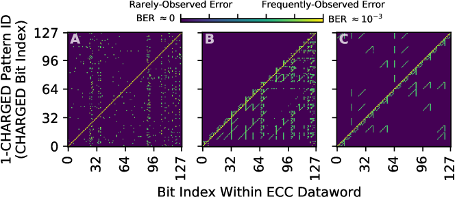
The data shows that miscorrection profiles vary significantly between different manufacturers. This is likely because each manufacturer uses a different parity-check matrix: the possible miscorrections for a given test pattern depend on which parity-check matrix columns are used to construct error syndromes. With different matrices, different columns combine to form different error syndromes. The miscorrection profiles of manufacturers B and C exhibit repeating patterns, which likely occur due to regularities in how syndromes are organized in the parity-check matrix, whereas the matrix of manufacturer A appears to be relatively unstructured. We suspect that manufacturers use different ECC functions because each manufacturer employs their own circuit design, and specific parity-check matrix organizations lead to more favorable circuit-level tradeoffs (e.g., layout area, critical path lengths).
We find that chips of the same model number from the same manufacturer yield identical miscorrection profiles, which (1) validates that we are observing design-dependent data and (2) confirms that chips from the same manufacturer and product generation appear to use the same ECC functions. To sanity-check our results, we use EINSim [467, 4] to simulate the miscorrection profiles of the final parity-check matrices we obtain from our experiments with real chips, and we observe that the miscorrection profiles obtained via simulation match those measured via real chip experiments.
6.4.2 Step 2: Analyzing Post-Correction Errors
In practice, BEER may either (1) fail to observe a possible miscorrection or (2) misidentify a miscorrection due to unpredictable transient errors (e.g., soft errors from particle strikes, variable-retention time errors, voltage fluctuations). These events can theoretically pollute the miscorrection profile with incorrect data, potentially resulting in an illegal miscorrection profile, i.e., one that does not match any ECC function.
Fortunately, case (1) is unlikely given the sheer number of ECC words even a single chip provides for testing (discussed in Section 6.4.1). While it is possible that different ECC words throughout a chip use different ECC functions, we believe that this is unlikely because it complicates the design with no clear benefits. Even if a chip does use more than one ECC function, the different functions will likely follow patterns aligning with DRAM substructures (e.g., alternating between DRAM rows or subarrays [315, 294]), and we can test each region individually.
Similarly, case (2) is unlikely because transient errors occur randomly and rarely [480] as compared with the data-retention error rates that we induce for BEER (), so transient error occurrence counts are far lower than those of real miscorrections that are observed frequently in miscorrection-susceptible bit positions. Therefore, we apply a simple threshold filter to remove rarely-observed post-correction errors from the miscorrection profile. Figure 6.3 shows the relative probability of observing a miscorrection in each bit position aggregated across all 1-CHARGED test patterns for a representative chip from manufacturer B. Each data point is a boxplot that shows the full distribution of probability values, i.e., min, median, max, and interquartile-range (IQR), observed when sweeping the refresh window from 2 to 22 minutes (i.e., the same experiments described in Section 6.4.1).
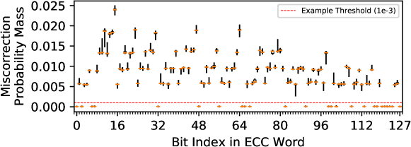
We see that zero and nonzero probabilities are distinctly separated, so we can robustly resolve miscorrections for each bit. Furthermore, each distribution is extremely tight, meaning that any of the individual experiments (i.e., any single component of the distributions) is suitable for identifying miscorrections. Therefore, a simple threshold filter (illustrated in Figure 6.3) distinctly separates post-correction errors that occur near-zero times from miscorrections that occur significantly more often.
6.4.3 Step 3: Solving for the ECC Function
We use the Z3 SAT solver [126] (described in Section LABEL:bg:sec:sat_solver) to identify the exact ECC function given a miscorrection profile. To determine the encoding () and decoding () functions, we express them as unknown generator (G) and parity-check (H) matrices, respectively. We then add the following constraints to the SAT solver for G and H:
-
1.
Basic linear code properties (e.g., unique H columns).
-
2.
Standard form matrices, as described in Section 6.3.2.
-
3.
Information contained within the miscorrection profile (i.e., pattern can(not) yield a miscorrection in bit ).
Upon evaluating the SAT solver with these constraints, the resulting G and H matrices represent the ECC encoding and decoding functions, respectively, that cause the observed miscorrection profile. To verify that no other ECC function may result in the same miscorrection profile, we simply repeat the SAT solver evaluation with the additional constraint that the already discovered G and H matrices are invalid. If the SAT solver finds another ECC function that satisfies the new constraints, the solution is not unique.
To seamlessly apply BEER to the DRAM chips that we test, we develop an open-source C++ application [1] that incorporates the SAT solver and determines the ECC function corresponding to an arbitrary miscorrection profile. The tool exhaustively searches for all possible ECC functions that satisfy the aforementioned constraints and therefore will generate the input miscorrection profile. Using this tool, we apply BEER to miscorrection profiles that we experimentally measure across all chips using refresh windows up to 30 minutes and temperatures up to 80∘C. We find that BEER uniquely identifies the ECC function for all manufacturers. Unfortunately, we are unable to publish the resulting ECC functions for confidentiality reasons as set out in Section 6.2.1. Although we are confident in our results because our SAT solver tool identifies a unique ECC function that explains the observed miscorrection profiles for each chip, we have no way to validate BEER’s results against a groundtruth. To overcome this limitation, we demonstrate BEER’s correctness using simulation in Section 6.5.1.
6.4.4 Requirements and Limitations
Although we demonstrate BEER’s effectiveness using both experiment and simulation, BEER has several testing requirements and limitations that we review in this section.
Testing Requirements
-
•
Single-level ECC: BEER assumes that there is no second level of ECC (e.g., rank-level ECC in the DRAM controller) present during testing.101010We can potentially extend BEER to multiple levels of ECC by extending the SAT problem to the concatenated code formed by the combined ECCs and constructing test patterns that target each level sequentially, but we leave this direction to future work. This is reasonable since system-level ECCs can typically be bypassed (e.g., via FPGA-based testing or disabling through the BIOS) or reverse-engineered [115], even in the presence of on-die ECC, before applying BEER.
-
•
Inducing data-retention errors: BEER requires finding a refresh window (i.e., ) for each chip that is long enough to induce data-retention errors and expose miscorrections. Fortunately, we find that refresh windows between 1-30 minutes at 80∘C reveal more than enough miscorrections to apply BEER. In general, the refresh window can be easily modified (discussed in Section 2.2.5), and because data-retention errors are fundamental to DRAM technology, BEER applies to all DDRx DRAM families regardless of their data access protocols and will likely hold for future DRAM chips, whose data-retention error rates will likely be even more prominent [405, 276, 435, 176, 332, 397, 448, 309, 538, 369].
Limitations
-
•
ECC code type: BEER works on systematic linear block codes, which are commonly employed for latency-sensitive main memory chips since: (i) they allow the data to be directly accessed without additional operations [629] and (ii) stronger codes (e.g., LDPC [158], concatenated codes [152]) cost considerably more area and latency [74, 444].
-
•
No groundtruth: BEER alone cannot confirm whether the ECC function that it identifies is the correct answer. However, if BEER finds exactly one ECC function that explains the experimentally observed miscorrection profile, it is very likely that the ECC function is correct.
-
•
Disambiguating equivalent codes: On-die ECC does not expose the parity-check bits, so BEER can only determine the ECC function to an equivalent code (discussed in Sections 6.3.2 and 6.3.2). Fortunately, equivalent codes differ only in their internal metadata representations, so this limitation should not hinder most third-party studies. In general, we are unaware of any way to disambiguate equivalent codes without accessing the ECC mechanism’s internals.
6.5 BEER Evaluation
We evaluate BEER’s correctness in simulation, SAT solver performance on a real system, and experimental runtime analytically. Our evaluations both (1) show that BEER is practical and correctly identifies the ECC function within our simulation-based analyses, and (2) provide intuition for how the SAT problem’s complexity scales for longer ECC codewords.
6.5.1 Simulation-Based Correctness Evaluation
We simulate applying BEER to DRAM chips with on-die ECC using a modified version of the EINSim [467, 4] open-source DRAM error-correction simulator that we also publicly release [4]. We simulate 115300 single-error correction Hamming code functions that are representative of those used for on-die ECC [229, 435, 405, 494, 448, 330, 331, 467]: 2000 each for dataword lengths between 4 and 57 bits, 100 each between 58 and 120 bits, and 100 each for selected values between 121 and 247 bits because longer codes require significantly more simulation time. For each ECC function, we simulate inducing data-retention errors within the 1-, 2-, and 3-CHARGED111111We include the 3-CHARGED patterns to show that they fail to uniquely identify all ECC functions despite comprising combinatorially more test patterns than the combined 1- and 2-CHARGED patterns. test patterns according to the data-retention error properties outlined in Section 2.2.5. For each test pattern, we model a real experiment by simulating ECC words and data-retention error rates ranging from to to obtain a miscorrection profile. Then, we apply BEER to the miscorrection profiles and show that BEER correctly recovers the original ECC functions.
Figure 6.4 shows how many unique ECC functions BEER finds when using different test patterns to generate miscorrection profiles. For each dataword length tested, we show the minimum, median, and maximum number of solutions identified across all miscorrection profiles. The data shows that BEER is always able to recover the original unique ECC function using the {1,2}-CHARGED configuration that uses both the 1-CHARGED and 2-CHARGED test patterns. For full-length codes (i.e., with dataword lengths ) that contain all possible error syndromes within the parity-check matrix by construction, all test patterns uniquely determine the ECC function, including the 1-CHARGED patterns alone.
On the other hand, the individual 1-, 2-, and 3-CHARGED patterns sometimes identify multiple ECC functions for shortened codes, with more solutions identified both for (1) shorter codes and (2) codes with more aggressive shortening. However, the data shows that BEER often still uniquely identifies the ECC function even using only the 1-CHARGED patterns (i.e., for 87.7% of all codes simulated) and always does so with the {1,2}-CHARGED patterns. This is consistent with the fact that shortened codes expose fewer error syndromes to test (discussed in Section 6.3.2). It is important to note that, even if BEER identifies multiple solutions, it still narrows a combinatorial-sized search space to a tractable number of ECC functions that are well suited to more expensive analyses (e.g., intrusive error-injection, die imaging techniques, or manual inspection).
While our simulations do not model interference from transient errors, such errors are rare events [480] when compared with the amount of uncorrectable data-retention errors that BEER induces. Even if sporadic transient errors were to occur, Section 6.4.2 discusses in detail how BEER mitigates their impact on the miscorrection profile using a simple thresholding filter.
6.5.2 Real-System Performance Evaluation
We evaluate BEER’s performance and memory usage using ten servers with 24-core 2.30 GHz Intel Xeon(R) Gold 5118 CPUs [227] and 192 GiB 2666 MHz DDR4 DRAM [249] each. All measurements are taken with Hyper-Threading [227] enabled and all cores fully occupied. Figure 6.5 shows overall runtime and memory usage when running BEER with the 1-CHARGED patterns for different ECC code lengths on a log-log plot along with the time required to (1) solve for the ECC function (“Determine Function”) and (2) verify the uniqueness of the solution (“Check Uniqueness”). Each data point gives the minimum, median, and maximum values observed across our simulated ECC functions (described in Section 6.5.1). We see that the total runtime and memory usage are negligible for short codes and grow as large as 62 hours and 11.4 GiB of memory for large codes. For a representative dataword length of 128 bits, the median total runtime and memory usage are 57.1 hours and 6.3 GiB, respectively. At each code length where we add an additional parity-check bit, the runtime and memory usage jump accordingly since the complexity of the SAT evaluation problem increases by an extra dimension.
The total runtime is quickly dominated by the SAT solver checking uniqueness, which requires exhaustively exploring the entire search space of a given ECC function. However, simply determining the solution ECC function(s) is much faster, requiring less than 2.7 minutes even for the longest codes evaluated and for shortened codes that potentially have multiple solutions using only the 1-CHARGED patterns. From this data, we conclude that BEER is practical for reasonable-length codes used for on-die ECC (e.g., ). However, our BEER implementation has room for optimization, e.g., using dedicated GF(2) BLAS libraries (e.g., LELA [214]) or advanced SAT solver theories (e.g., SMT bitvectors [72]), and an optimized implementation would likely improve performance, enabling BEER’s application to an even greater range of on-die ECC functions. Section 9.1.1 discusses such optimizations in greater detail. Nevertheless, BEER is a one-time offline process, so it need not be aggressively performant in most use-cases.
6.5.3 Analytical Experiment Runtime Analysis
Our experimental runtime is overwhelmingly bound by waiting for data-retention errors to occur during a lengthened refresh window (e.g., 10 minutes) while interfacing with the DRAM chip requires only on the order of milliseconds (e.g., 168 ms to read an entire 2 GiB LPDDR4-3200 chip [250]). Therefore, we estimate total experimental runtime as the sum of the refresh windows that we individually test. For the data we present in Section 6.4.1, testing each refresh window between 2 to 22 minutes in 1 minute increments requires a combined 4.2 hours of testing for a single chip. However, if chips of the same model number use the same ECC functions (as our data supports in Section 6.4.1), we can reduce overall testing latency by parallelizing individual tests across different chips. Furthermore, because BEER is likely a one-time exercise for a given DRAM chip, it is sufficient that BEER is practical offline.
6.6 Example Practical Use-Cases
BEER empowers third-party DRAM users to decouple the reliability characteristics of modern DRAM chips from any particular on-die ECC function that a chip implements. This section discusses five concrete analyses that BEER enables. To our knowledge, BEER is the first work capable of inferring this information without bypassing the on-die ECC mechanism. We hope that end users and future works find more ways to extend and apply BEER in practice.
6.6.1 BEEP: Profiling for Raw Bit Errors
We introduce Bit-Exact Error Profiling (BEEP), a new data-retention error profiling algorithm enabled by BEER that infers the number and bit-exact locations of pre-correction error-prone cells when given a set of operating conditions that cause uncorrectable errors in an ECC word. To our knowledge, BEEP is the first DRAM error profiling methodology capable of identifying bit-exact error locations throughout the entire on-die ECC codeword, including within the parity bits.
BEEP: Inference Based on Miscorrections
Because miscorrections are purely a function of the ECC logic (discussed in Section 6.3.2), an observed miscorrection indicates that a specific pre-correction error pattern has occurred. Although several such patterns can map to the same miscorrection, BEEP narrows down the possible pre-correction error locations by using the known parity-check matrix (after applying BEER) to construct test patterns for additional experiments that disambiguate the possibilities. At a high level, BEEP crafts test patterns to reveal errors as it incrementally traverses each codeword bit, possibly using multiple passes to capture low-probability errors. As BEEP iterates over the codeword, it builds up a list of suspected error-prone cells.
BEEP comprises three phases: crafting suitable test patterns, experimental testing with crafted patterns, and calculating pre-correction error locations from observed miscorrections. Figure 6.6 illustrates these three phases in an example where BEEP profiles for pre-correction errors in a 128-bit ECC dataword. The following sections explain each of the three phases and refer to Figure 6.6 as a running example.
Crafting Suitable Test Patterns
Conventional DRAM error profilers (e.g., [571, 370, 369, 283, 346, 468, 285, 103, 564, 327, 199, 259]) use carefully designed test patterns that induce worst-case circuit conditions in order to maximize their coverage of potential errors [12, 414]. Unfortunately, on-die ECC encodes all data into codewords, so the intended software-level test patterns likely do not maintain their carefully-designed properties when written to the physical DRAM cells. BEEP circumvents these ECC-imposed restrictions by using a SAT solver along with the known ECC function (via BEER) to craft test patterns that both (1) locally induce the worst-case circuit conditions and (2) result in observable miscorrections if suspected error-prone cells do indeed fail.
Without loss of generality, we assume that the worst-case conditions for a given bit occur when its neighbors are programmed with the opposite charge states, which prior work shows to exacerbate circuit-level coupling effects and increase error rates [12, 369, 283, 414, 565, 488, 21, 521, 324, 362, 436]. If the design of a worst-case pattern is not known, or if it has a different structure than we assume, BEEP can be adapted by simply modifying the relevant SAT solver constraints (described below). To ensure that BEEP observes a miscorrection when a given error occurs, BEEP crafts a pattern that will suffer a miscorrection if the error occurs alongside an already-discovered error. We express these conditions to the SAT solver using the following constraints:
-
1.
Bits adjacent to the target bit have opposing charge states.
-
2.
One or more miscorrections is possible using some combination of the already-identified data-retention errors.
Several such patterns typically exist, and BEEP simply uses the first one that the SAT solver returns (although a different BEEP implementation could test multiple patterns to help identify low-probability errors). Figure 6.6 illustrates how such a test pattern appears physically within the cells of a codeword: the target cell is CHARGED, its neighbors are DISCHARGED, and the SAT solver freely determines the states of the remaining cells to increase the likelihood of a miscorrection if the target cell fails. If the SAT solver fails to find such a test pattern, BEEP attempts to craft a pattern using constraint 2 alone, which, unlike constraint 1, is essential to observing miscorrections. Failing that, BEEP simply skips the bit until more error-prone cells are identified that could facilitate causing miscorrections. We evaluate how successfully BEEP identifies errors in Section 6.6.1, finding that a second pass over the codeword helps in cases of few or low-probability errors.
Experimental Testing with Crafted Patterns
BEEP tests a pattern by writing it to the target ECC word, inducing errors by lengthening the refresh window, and reading out the post-correction data. Figure 6.6 shows examples of post-correction error patterns that might be observed during an experiment. Each miscorrection indicates that an uncorrectable number of pre-correction errors exists, and BEEP uses the parity-check matrix H to calculate their precise locations. This is possible because each miscorrection reveals an error syndrome for the (unknown) erroneous pre-correction codeword that caused the miscorrection. Therefore, we can directly solve for as shown in Equation 6.3.
| (6.3) |
This is a system of equations with one equation for each of unknowns, i.e., one each for the inaccessible parity bits. There is guaranteed to be exactly one solution for since the parity-check matrix always has full rank (i.e., ). Since we also know the original codeword (), we can simply compare the two (i.e., ) to determine the bit-exact error pattern that led to the observed miscorrection. Figure 6.6 shows how BEEP updates a list of learned pre-correction error locations, which the SAT solver then uses to construct test patterns for subsequent bits. Once all bits are tested, the list of pre-correction errors yields the number and bit-locations of all identified error-prone cells.
Evaluating BEEP’s Success Rate
To understand how BEEP performs in practice, we evaluate its success rate, i.e., the likelihood that BEEP correctly identifies errors within a codeword. We use a modified version of EINSim [4] to perform Monte-Carlo simulation across 100 codewords per measurement. To keep our analysis independent of any particular bit-error rate model, we subdivide experiments by the number of errors () injected per codeword. In this way, we can flexibly evaluate the success rate for a specific error distribution using the law of total probability over the s.
Number of Passes. Figure 6.7 shows BEEP’s success rate when using one and two passes over the codeword for different codeword lengths. Each bar shows the median value over the 100 codewords with an error bar showing the 5th and 95th percentiles. The data shows that BEEP is highly successful across all tested error counts, especially for longer 127- and 255-bit codewords that show a 100% success rate even with a single pass. Longer codewords perform better in part because BEEP uses one test pattern per bit, which means that longer codes lead to more patterns. However, longer codewords perform better even with comparable test-pattern counts (e.g., 2 passes with 31-bit vs 1 pass with 63-bit codewords) because longer codewords simply have more bits (and therefore, error syndromes) for the SAT solver to consider when crafting a miscorrection-prone test pattern. On the other hand, miscorrection-prone test patterns are more difficult to construct for shorter codes that provide fewer bits to work with, so BEEP fails more often when testing shorter codes.
Per-Bit Error Probabilities. Figure 6.8 shows how BEEP’s success rate changes using a single pass when the injected errors have different per-bit probabilities of error (P[error]). This experiment represents a more realistic scenario where some DRAM cells probabilistically experience data-retention errors. We see that BEEP remains effective (i.e., has a near-100% success rate) for realistic 63- and 127-bit codeword lengths, especially at higher bit-error probabilities and error counts. BEEP generally has a higher success rate with longer codes compared to shorter ones, and for shorter codewords at low error probabilities, the data shows that BEEP may require more test patterns (e.g., multiple passes) to reliably identify all errors.
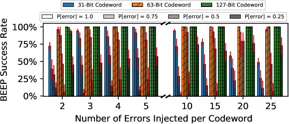
It is important to note that, while evaluating low error probabilities is demonstrative, it represents a pessimistic scenario since a real DRAM chip exhibits a mix of low and high per-bit error probabilities.121212Patel et al. [468] provide a preliminary exploration of how per-bit error probabilities are distributed throughout a DRAM chip, but formulating a detailed error model for accurate simulation is beyond the scope of our work. Although any error-profiling mechanism that identifies errors based on when they manifest might miss low-probability errors,131313Patel et al. [468] increase error coverage by exacerbating the bit-error probability, and their approach (REAPER) can be used alongside BEEP to help identify low-probability errors. the data shows that BEEP is resilient to low error probabilities, especially for longer, more realistic codewords. Therefore, our evaluations demonstrate that BEEP effectively enables a new profiling methodology that uses the ECC function determined by BEER to infer pre-correction errors from observed post-correction error patterns.
Other DRAM Error Mechanisms
Although we demonstrate BEEP solely for data-retention errors, BEEP can potentially be extended to identify errors that occur due to other DRAM error mechanisms (e.g., stuck-at faults, circuit timing failures). However, simultaneously diagnosing multiple error models is a very difficult problem since different types of faults can be nearly indistinguishable (e.g., data-retention errors and stuck-at-DISCHARGED errors). Profiling for arbitrary error types is a separate problem from what we tackle in this work, and we intend BEEP as a simple, intuitive demonstration of how knowing the ECC function is practically useful. Therefore, we leave extending BEEP to alternative DRAM error mechanisms to future work.
6.6.2 Other Use-Cases that Benefit from BEER
We identify four additional use cases for which BEER mitigates on-die ECC’s interference with third-party studies by revealing the full ECC function (i.e., its parity-check matrix).
Combining Error Mitigation Mechanisms
If the on-die ECC function is known, a system architect can design a second level of error mitigation (e.g., rank-level ECC) that better suits the error characteristics of a DRAM chip with on-die ECC. Figure 1 provides a simple example of how different ECC functions cause different data bits to be more error-prone even though the pre-correction errors are uniformly distributed. This means that on-die ECC changes the DRAM chip’s software-visible error characteristics in a way that depends on the particular ECC function it employs. If the on-die ECC function is known, we can calculate the expected post-correction error characteristics141414By assuming a given data value distribution, e.g., fixed values for a predictable software application, uniform-random data for a general system. and build an error model that accounts for the transformative effects of on-die ECC. Using this error model, the system architect can make an informed decision when selecting a secondary mitigation mechanism to complement on-die ECC. For example, architects could modify a traditional rank-level ECC scheme to asymmetrically protect certain data bits that are more prone to errors than others as a result of on-die ECC’s behavior [327, 592]. In general, BEER enables system designers to better design secondary error-mitigation mechanisms to suit the expected DRAM reliability characteristics, thereby improving overall system reliability.
Crafting Targeted Test Patterns
Several DRAM error mechanisms are highly pattern sensitive, including RowHammer [312, 422, 426, 297], data-retention [468, 369, 370, 282, 283, 285, 191, 305], and reduced-access-latency [294, 346, 343, 91, 94]. Different test patterns affect error rates by orders of magnitude [337, 369, 468, 297, 285, 283, 284] because each pattern exercises different static and dynamic circuit-level effects. Therefore, test patterns are typically designed carefully to induce the worst-case circuit conditions for the error mechanism under test (e.g., marching ‘1’s [12, 369, 468, 199, 414]). As Section 6.6.1 discusses in greater detail, on-die ECC restricts the possible test patterns to only the ECC function’s codewords. Fortunately, the SAT-solver-based approach that BEEP uses to craft test patterns generalizes to crafting targeted test patterns for these error mechanisms also.
Studying Spatial Error Distributions
Numerous prior works [526, 312, 91, 460, 346, 294, 94] experimentally study the spatial distributions of errors throughout the DRAM chip in order to gain insight into how the chip operates and how its performance, energy, and/or reliability can be improved. These studies rely on inducing errors at relatively high error rates so that many errors occur that can leak information about a device’s underlying structure. With on-die ECC, studying spatial error distributions requires identifying pre-correction errors throughout the codeword, including within the inaccessible parity bits. BEEP demonstrates one possible concrete way by which BEER enables these studies for chips with on-die ECC.
Diagnosing Post-Correction Errors
A third-party tester may want to determine the physical reason(s) behind an observed error. For example, a system integrator who is validating a DRAM chip’s worst-case operating conditions may observe unexpected errors due to an unforeseen defect (e.g., at a precise DQ-pin position). Unfortunately, on-die ECC obscures both the number and locations of pre-correction errors, so the observed errors no longer provide insight into the underlying physical error mechanism responsible. Using BEEP, such errors can be more easily diagnosed because the revealed pre-correction errors directly result from the error mechanism.
6.7 Summary
We introduce Bit-Exact Error Recovery (BEER), a new methodology for determining the full DRAM on-die ECC function (i.e., its parity-check matrix) without requiring hardware support, prerequisite knowledge about the DRAM chip or on-die ECC mechanism, or access to ECC metadata (e.g., parity-check bits, error syndromes). We use BEER to determine the on-die ECC functions of 80 real LPDDR4 DRAM chips and show that BEER is both effective and practical using rigorous simulations. We discuss five concrete use-cases for BEER, including BEEP, a new DRAM error profiling methodology capable of inferring exact pre-correction error counts and locations. We believe that BEER takes an important step towards enabling effective third-party design and testing around DRAM chips with on-die ECC and are hopeful that BEER will enable many new studies going forward.
?chaptername? 7 Practical and Effective Error Profiling for Memory Chips with On-Die ECC
Throughout the previous three chapters, we built a detailed understanding of how and why on-die ECC obfuscates pre-correction errors. Then, we developed new testing techniques that provide insight into the on-die ECC mechanism and the pre-correction errors. In this chapter, we closely study the characteristics of the post-correction errors. We examine how and why on-die ECC makes error profiling difficult from outside of the memory chip, regardless of whether a profiler knows the details of the on-die ECC implementation. Then, we develop a new error profiling algorithm, Hybrid Active-Reactive Profiling (HARP) to overcome the challenges that on-die ECC introduces for practical and effective error profiling.
7.1 Background and Motivation
Modern memory technologies that are suitable for main memory (e.g., Dynamic Random Access Memory (DRAM) [132, 384], Phase-Change Memory (PCM) [339, 340, 598, 73, 341, 481], Spin-Transfer Torque RAM (STT-RAM) [217, 328]) all suffer from various error mechanisms that play a key role in determining reliability, manufacturing yield, and operating characteristics such as performance and energy efficiency [355, 632, 239, 73, 581, 339, 340, 328, 276, 461, 88, 297, 384, 341, 184]. Unfortunately, as memory designers shrink (i.e., scale) memory process technology node sizes to meet ambitious capacity, cost, performance, and energy efficiency targets, worsening reliability becomes an increasingly significant challenge to surmount [355, 33, 420, 570, 88, 461, 276, 434, 480, 312, 426, 297, 211, 384, 304]. For example, DRAM process technology scaling exacerbates cell-to-cell variation and noise margins, severely impacting error mechanisms that constrain yield, including cell data-retention [369, 434, 321, 283, 276, 571, 190, 191, 461, 88, 211, 468, 282, 526] and read-disturb [312, 297, 426, 422, 154, 455, 198] phenomena. Similarly, emerging main memory technologies suffer from various error mechanisms that can lead to high error rates if left unchecked, such as limited endurance, resistance drift, and write disturbance in PCM [339, 340, 358, 306, 239, 275, 33] and data retention, endurance, and read disturbance in STT-RAM [570, 97, 29, 430, 110, 487]. Therefore, enabling reliable system operation in the presence of scaling-related memory errors is a critical research challenge for allowing continued main memory scaling.
Error mitigation mechanisms and on-die ECC. Modern systems tolerate errors using error-mitigation mechanisms, which prevent errors that occur within the memory chip from manifesting as software-visible bit flips. Different error-mitigation mechanisms target different types of errors, ranging from fine- to coarse-grained mitigation using hardware and/or software techniques. section 2.3 reviews main memory error-mitigation mechanisms.
To address increasing memory error rates, memory chip manufacturers have started to incorporate on-die error-correcting codes (on-die ECC).111Our work applies to any memory chip that is packaged with a proprietary ECC mechanism; on-die ECC is one embodiment of such a chip. On-die ECC is already prevalent among modern DRAM (e.g., LPDDR4 [405, 447, 330, 331, 467, 466], DDR5 [253]) and STT-RAM [144] chips because it enables memory manufacturers to aggressively scale their technologies while maintaining the appearance of a reliable memory chip. Unfortunately, on-die ECC changes how memory errors appear outside the memory chip (e.g., to the memory controller or the system software). This introduces new challenges for designing additional error-mitigation mechanisms at the system level [538, 177, 435, 258, 88, 456, 119, 381, 185] or test a memory chip’s reliability characteristics [467, 466, 170, 179].
In this work, we focus on enabling a class of state-of-the-art hardware-based error-mitigation mechanisms known as repair mechanisms222We discuss repair mechanisms in detail in section 2.3.4. [615, 434, 231, 507, 366, 556, 320, 373, 321, 432, 511, 594, 622, 370, 480, 571, 538] when used alongside memory chips with on-die ECC. These repair mechanisms operate from outside the memory chip (e.g., from the memory controller) to identify and repair memory locations that are at risk of error (i.e., are known or predicted to experience errors). In particular, prior works [434, 320, 556, 507, 511] show that bit-granularity repair mechanisms efficiently tackle high error rates (e.g., ) resulting from aggressive technology scaling by focusing error-mitigation resources on bits that are known to be susceptible to errors.
Fig. 7.1 illustrates a system that uses both a repair mechanism (within the memory controller) and on-die ECC (within the memory chip). On-die ECC encodes all data provided by the CPU before writing it to the memory. On a read operation, on-die ECC first decodes the stored data, correcting any correctable errors. The repair mechanism then repairs the data before returning it to the CPU. The repair mechanism performs repair operations using a list of bits known to be at risk of error, called an error profile.
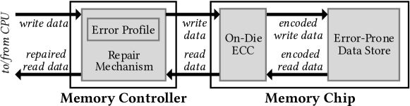
7.1.1 Motivation: Understanding and Overcoming Profiling Challenges Introduced by On-Die ECC
Repair mechanisms depend on having a practical algorithm for identifying at-risk memory locations to repair. We refer to this as an error profiling algorithm. We classify a profiling algorithm as either active or reactive depending on whether it takes action to search for at-risk memory locations or passively monitors memory to identify errors as they occur during normal system operation. Prior works [571, 370, 282, 284, 283, 285, 468, 480, 107, 346, 35, 523, 297, 154, 115, 631, 192, 556, 478, 466, 369, 113, 426, 94, 343, 294, 296, 37, 300, 366] propose a variety of algorithms for active profiling. In general, these algorithms all search for errors using multiple rounds of tests that each attempt to induce and identify errors (e.g., by taking exclusive control of the memory chip [556, 369, 468, 466]). The algorithms maximize the chance of observing errors to identify as many at-risk bits as possible by testing under worst-case conditions (e.g., data and access patterns, operating conditions). Only BEEP [466] accounts for the effects of on-die ECC by first reverse-engineering the on-die ECC implementation, so we refer to all other active profiling algorithms as Naive in the context of this work. In contrast, proposals for reactive profiling passively monitor an error-detection mechanism (typically an ECC) to identify errors as they occur during normal system operation [240, 417, 480, 523, 478, 398, 45, 499].
Regardless of the profiling algorithm, any at-risk bits that the profiler misses will not be repaired by the repair mechanism that the profiler supports. Therefore, achieving practical and effective repair requires a profiling algorithm that quickly and efficiently achieves high coverage of at-risk memory locations.
On-die ECC’s impact on error profiling. Unfortunately, on-die ECC fundamentally changes how memory errors appear outside of the memory chip: instead of errors that follow well-understood semiconductor error models [252], the system observes obfuscated error patterns that vary with the particular on-die ECC implementation [467, 466]. This is a serious challenge for existing profiling algorithms because, as section 7.3 shows, on-die ECC both (1) increases the number of at-risk bits that need to be identified and (2) makes those bits harder to identify. Even a profiler that knows the on-die ECC implementation (e.g., BEEP [466]) cannot easily identify all at-risk bits because it lacks visibility into the error-correction process.
Our goal is to study and address the challenges that on-die ECC introduces for bit-granularity error profiling. To this end, we perform the first analytical study of how on-die ECC affects error profiling. We find that on-die ECC introduces statistical dependence between errors in different bit positions such that, even if raw bit errors (i.e., pre-correction errors) occur independently, errors observed by the system (i.e., post-correction errors) do not. This raises three new challenges for practical and effective bit-granularity error profiling (discussed in detail in section 7.3).
First, on-die ECC transforms a small set of bits at risk of pre-correction errors into a combinatorially larger set of bits at risk of post-correction errors. section 7.3.1 shows how this exponentially increases the number of bits the profiler must identify. Second, on-die ECC ties post-correction errors to specific combinations of pre-correction errors. Only when those specific pre-correction error combinations occur, can the profiler identify the corresponding bits at risk of post-correction errors. section 7.3.2 shows how this significantly slows down profiling. Third, on-die ECC interferes with commonly-used memory data patterns that profilers use to maximize the chance of observing errors. This is because post-correction errors appear only when multiple pre-correction errors occur concurrently, which the data patterns must account for. section 7.3.3 discusses the difficulty of defining new data patterns for use with on-die ECC.
7.1.2 Mechanism: Hybrid Active-Reactive Profiling (HARP)
To address these three challenges, we introduce Hybrid Active-Reactive Profiling (HARP), a new bit-granularity error profiling algorithm that operates within the memory controller to support a repair mechanism for memory chips with on-die ECC. HARP is based on two key insights. First, given that on-die ECC uses systematic encoding (i.e., data bits are preserved one-to-one during ECC encoding333Nonsystematic designs require additional decoding effort (i.e., more logic operations) because data cannot be read directly from stored values [628]. This increases the energy consumption of read operations and either reduces the overall read timing margins available for other memory operations or increases the memory read latency.), there are only two possible types of post-correction errors: (1) direct errors, corresponding to pre-correction errors within the systematically encoded data bits; and (2) indirect errors, resulting from mistaken correction operations (i.e., miscorrections) on-die ECC performs for uncorrectable errors. Second, because on-die ECC corrects a fixed number of errors, at most indirect errors can occur concurrently (e.g., for a Hamming code [193]).
Based on these insights, the key idea of HARP is to reduce the problem of profiling a chip with on-die ECC into that of a chip without on-die ECC by separately identifying direct and indirect errors. HARP consists of two phases. First, an active profiling phase that uses existing profiling techniques to identify bits at risk of direct errors with the help of a simple modification to the on-die ECC read operation that allows the memory controller to read raw data (but not the on-die ECC metadata) values. Second, a reactive profiling phase that safely identifies bits at risk of indirect errors using a secondary -error-correcting ECC within the memory controller. The secondary ECC is used only for reactive profiling: upon identifying an error, the corresponding bit is marked as at-risk, which signals the repair mechanism to repair the bit thereafter.
Prior work [466] shows that knowing the on-die ECC’s internal implementation (i.e., its parity-check matrix)444Potentially provided through manufacturer support, datasheet information, or previously-proposed reverse engineering techniques [466]. enables calculating which post-correction errors a given set of pre-correction errors can cause. Therefore, we introduce two HARP variants: HARP-Aware (HARP-A) and HARP-Unaware (HARP-U), which do and do not know the parity-check matrix, respectively. HARP-A does not improve coverage over HARP-U because it has no additional visibility into the pre-correction errors. However, HARP-A demonstrates that, although knowing the parity-check matrix alone does not overcome the three profiling challenges, it does provide a head-start for reactive profiling based on the results of active profiling.
We evaluate HARP in simulation relative to two state-of-the-art baseline error profiling algorithms: Naive (which represents the vast majority of previous-proposed profiling algorithms [571, 370, 282, 284, 283, 285, 468, 480, 107, 346, 35, 523, 297, 154, 115, 631, 192, 556, 478, 466, 369, 113, 426, 94, 343, 294, 296, 37, 300, 366]) and BEEP [466]. We show that HARP quickly achieves coverage of all bits at risk of direct errors while Naive and BEEP are either slower or unable to achieve full coverage. For example, when there are 2/3/4/5 bits at risk of pre-correction error that each fail with probability 0.5, HARP555HARP-U and HARP-A have identical coverage of bits at risk of direct error. achieves 99th-percentile666We report 99th percentile coverage to compare against baseline configurations that do not achieve full coverage within the maximum simulated number of profiling rounds (due to simulation time constraints, as discussed in section 7.6.1). coverage in 20.6%/36.4%/52.9%/62.1% of the profiling rounds required by the best baseline algorithm. Based on our evaluations, we conclude that HARP effectively overcomes the three profiling challenges. We publicly release our simulation tools as open-source software on Zenodo [469] and Github [5].
To demonstrate the end-to-end importance of having an effective profiling mechanism, we also perform a case study of how HARP, Naive, and BEEP profiling can impact the overall bit error rate of a system equipped with an ideal bit-repair mechanism that perfectly repairs all identified at-risk bits. We show that, because HARP achieves full coverage of bits at risk of direct errors, it enables the bit-repair mechanism to repair all errors. Although Naive eventually achieves full coverage, it takes substantially longer to do so (by for a raw per-bit error probability of 0.75). In contrast, BEEP does not achieve full coverage, so the bit-repair mechanism is unable to repair all errors that occur during system operation.
7.2 Formalizing Error Profiling
We express error profiling as a statistical process to understand the effects of on-die ECC. To this end, we first formalize the concepts of errors and error profiling. Then, we examine how on-die ECC changes the way that errors appear outside of the memory chip.
7.2.1 Practical and Effective Error Profiling
Any repair mechanism’s effectiveness strongly depends on the effectiveness of the error profiling algorithm that it uses because the repair mechanism can only repair memory locations that it knows are at risk of error. In this section, we define the key properties of practical and effective active and reactive profilers.
Active Profiling.
Active profiling algorithms take exclusive control of a memory chip in order to (possibly destructively) test worst-case data and access patterns [571, 370, 284, 283, 285, 468, 346, 35, 297, 154, 115, 631, 192], so the system cannot perform useful work while profiling. Therefore, an active profiler must identify at-risk bits as quickly and comprehensively as possible. We quantify this by measuring the fraction of all at-risk bits that a given profiler identifies (i.e., its coverage) across a fixed number of testing rounds.
Reactive Profiling.
Reactive profiling algorithms (e.g., ECC scrubbing [194, 480, 107, 523, 23, 430]) passively monitor error-detection mechanisms during normal system operation, so their performance and energy impact is relatively low and can be amortized across runtime [194, 480]. However, because reactive profilers operate during runtime, they must ensure that they can not only detect, but also correct any errors that occur. Any errors that are not detected and corrected by the reactive profiler risk introducing failures to the rest of the system. In our work, we quantify the error-mitigation capability of a reactive profiler in terms of ECC correction capability, which is well-defined for ECCs used in memory hardware design (i.e., linear block codes [495, 492, 212]).
7.2.2 Errors and Error Models
Our work assumes uncorrelated single-bit errors because recent experimental studies and repair efforts from academia [434, 54, 373, 432, 538], industry [276], and memory manufacturers themselves [405, 230, 231, 88, 461] focus on single-bit errors as the primary reliability challenge with increasing storage density. In particular, DRAM and STT-RAM manufacturers use on-die ECC specifically to combat these errors in recent high-density chips [177, 405, 230, 276, 447, 144, 88]. Therefore, we assume that errors exhibit the following properties:
-
1.
Bernoulli process: independent of previous errors.
-
2.
Isolated: independent of errors in other bits.
-
3.
Data-dependent: dependent on the stored data pattern.
To first order, this error model suits a broad range of error mechanisms that relate to technology scaling and motivate the use of bit-granularity repair, including DRAM data-retention [571, 190, 191, 369, 434, 320, 321, 283, 37, 468, 589, 266, 264, 305, 323, 364] and read disturbance [312, 297, 460]; PCM endurance, resistance drift, and write disturbance [507, 339, 340, 358, 306, 239, 275]; and STT-RAM data retention, endurance, and read disturbance [570, 97, 29, 430, 110, 487]. We use DRAM data-retention errors in our evaluations as a well-studied and relevant example. However, a profiler is fundamentally agnostic to the underlying error mechanism; it identifies at-risk bits based on whether or not they are observed to fail during profiling. Therefore, our analysis applies directly to any error mechanism that can be described using the aforementioned three properties.
Correlated Errors. Prior DRAM studies show evidence of correlated errors [20, 397, 547, 541, 542, 540]. However, we are not aware of evidence that such errors are a first-order concern of modern DRAM technology scaling. Correlated errors often result from faults outside the memory array [397] and are mitigated using fault-specific error-mitigation mechanisms (e.g., write CRC [332, 249], chipkill [129, 26, 435] or even stronger rank-level ECC [547, 249, 301]).
Low-Probability Errors. Other main memory error mechanisms exist that do not conform to our model, including time-dependent errors such as DRAM variable retention time [608, 491, 410, 526, 369, 282, 480] and single-event upsets such as particle strikes [391]. In general, these errors are either (1) inappropriate to address using a profile-guided repair mechanism, e.g., single-event upsets that do not repeat; or (2) rare or unpredictable enough that no realistic amount of active profiling is likely to identify them, so they are left to reactive profiling for detection and/or mitigation [480]. Identifying low-probability errors is a general challenge for any error profiler and is an orthogonal problem to our work. Prior approaches to identifying low-probability errors during active (e.g., increasing the probability of error [468]) or reactive (e.g., periodic ECC scrubbing [33, 480]) profiling are complementary to our proposed techniques and can be combined with HARP (e.g., during the active profiling phase described in section 7.5.2, or by strengthening the secondary ECC as described in section 7.5.3) to help identify low-probability errors.
7.2.3 Representing the Probability of Error
We model memory as a one-dimensional bit-addressable array with address space . To describe errors within this address space, we define two Boolean random variables and that represent the data stored in bit and whether or not the bit experiences an error, respectively. Based on our discussion in section 7.2.2, we model as a Bernoulli random variable that is independent of but dependent on the data . In general, can depend on the data stored in other cells , which expresses how a bit’s probability of error changes with the data stored in nearby cells. Equation 7.1 shows the resulting probability mass function, parameterized by , the probability that the bit will experience an error.
| (7.1) |
In general, each bit has its own value of depending on its intrinsic error characteristics. For example, prior work [468] experimentally demonstrates that values are normally distributed across different bits for DRAM data-retention errors, i.e., , with some normal distribution parameters that depend on the particular memory chip and operating conditions such as temperature.
7.2.4 Incorporating On-Die ECC
With on-die ECC, we adjust our address space representation to include both logical bit addresses as observed by the memory controller and physical bit addresses within the memory storage array. In general, because includes addresses for parity-check bits that are not visible outside of the memory chip. Next, we introduce two additional Boolean random variables: (for dataword) and (for codeword) that refer to the data values of logical bit and physical bit (i.e., before and after ECC encoding), respectively. Boolean variables and represent whether logical bit and physical bit experience post- and pre-correction errors, respectively. Note that and represent the same information from section 7.2.3. We use and to refer to codeword and dataword values, respectively, that may contain errors.
On-die ECC determines from through syndrome decoding (described in LABEL:bg:subsec:ondieecc_hamming_code) using the ECC parity-check matrix comprised of columns . The error syndrome is computed as (referred to as to simplify notation). Then, if matches the ’th column , the ECC decoder flips the bit at position . Given that is systematically encoded (discussed in LABEL:bg:subsec:ondieecc_hamming_code), is equal to . Therefore, a post-correction error (i.e., a mismatch between and ) can only occur in two cases: (1) an uncorrected raw bit error at position (i.e., ); or (2) a miscorrection at position (i.e., .) We refer to these two cases as direct and indirect errors, respectively. Equation 7.2 summarizes both cases that lead to a post-correction error.
| (7.2) |
Equation 7.2 shows that bit ’s probability of error depends not only on that of its encoded counterpart , but also on those of all other codeword bits . This means that on-die ECC introduces statistical dependence between all bits in a given ECC word through their mutual dependence on . Furthermore, just as described in section 7.2.3, itself depends on the data value stored in cell (i.e., ). As a result, bit ’s probability of error depends on both the data values and the pre-correction errors present throughout the codeword.
Consequently, a given post-correction error may only occur when a particular combination of pre-correction errors occurs. This is different from the case without on-die ECC, where does not depend on the data or error state of any other bit . We conclude that on-die ECC transforms statistically independent pre-correction errors into ECC-dependent, correlated post-correction errors.
7.3 On-Die ECC’s Impact on Profiling
On-die ECC breaks the simple and intuitive assumption that profiling for errors is the same as profiling each bit individually. In this section, we identify three key challenges that on-die ECC introduces for bit-granularity profiling.
7.3.1 Challenge 1: Combinatorial Explosion
section 7.2.4 shows that the position of an indirect error depends on the locations of all pre-correction errors . This means that different uncorrectable patterns of pre-correction errors can cause indirect errors in different bits. In the worst case, every unique combination of pre-correction errors within a set of at-risk bits can lead to different indirect errors. This means that the set of bits that are at risk of post-correction errors is combinatorially larger than the set of bits at risk of pre-correction error.
As a concrete example, Fig. 7.2 shows a violin plot of each at-risk bit’s per-bit probability of error (y-axis) when the codeword contains a fixed number of bits at risk of pre-correction errors (x-axis) that each fail with probability . Each violin shows the distribution (median marked in black) of per-bit error probabilities when simulating 70,000 ECC words for each of 1600 randomly-generated (71, 64) Hamming code parity-check matrices assuming a data pattern of 0xFF. We make two observations. First, the pre-correction error probabilities are all 0.5 (by design). This means that, without on-die ECC, all bits at risk of pre-correction error are easy to identify, i.e., each bit will be identified with probability given profiling rounds. For large (e.g., , where ), the vast majority of bits will be identified.
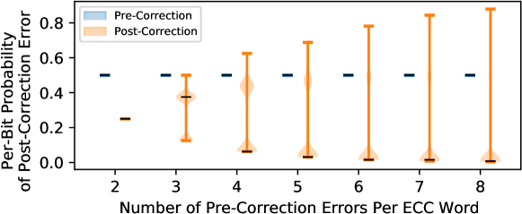
Second, in contrast, the per-bit probabilities of post-correction error exhibit a wide range. However, the probability density for each violin is tightly concentrated at for and shifts towards as the number of pre-correction errors increases. This means that the bits at risk of post-correction errors become harder to identify because they fail less often.
Table 7.1 shows the maximum number of bits at risk of post-correction errors that can be caused by a fixed number of bits at risk of pre-correction errors. This illustrates the worst-case scenario, where every uncorrectable combination of pre-correction errors (i.e., pre-correction error pattern) causes a unique indirect error. We see that bits at risk of pre-correction errors can cause unique pre-correction error patterns. Of these, are correctable error patterns, leaving uncorrectable pre-correction error patterns. Assuming that each of these patterns introduces a unique indirect error, the combination of bits at risk of direct and indirect error leads to bits at risk of post-correction errors. Therefore, we conclude that on-die ECC exponentially increases the number of at-risk bits that the profiler must identify.
| Bits at risk of pre-correction errors | 1 | 2 | 3 | 4 | 8 | |
|---|---|---|---|---|---|---|
| Unique pre-correction error patterns | 1 | 3 | 7 | 15 | 255 | |
| Uncorrectable pre-correction error patterns | 0 | 2 | 4 | 11 | 247 | |
| Bits at risk of post-correction errors | 1 | 3 | 7 | 15 | 255 |
7.3.2 Challenge 2: Profiling without Feedback
Without on-die ECC, an at-risk bit is identified when the bit fails. This means that every profiling round provides useful feedback about which bits are and are not at risk of error. Unfortunately, with on-die ECC, a bit at risk of post-correction errors can only be identified when particular combination(s) of pre-correction errors occur. This has two negative consequences.
First, because the profiler cannot observe pre-correction errors, it does not know whether a particular combination of pre-correction errors has been tested yet. Therefore, the profiler cannot draw meaningful conclusions from observing a bit not to fail. Instead, the profiler must pessimistically suspect every bit to be at risk of post-correction errors, even after many profiling rounds have elapsed without observing a given bit fail. Second, each ECC word can only exhibit one pre-correction error pattern at a time (i.e., during any given profiling round). This serializes the process of identifying any two bits at risk of post-correction errors that fail under different pre-correction error patterns.
As a result, no profiler that identifies at-risk bits based on observing post-correction errors can quickly identify all bits at risk of post-correction errors. We refer to this problem as bootstrapping because the profiler must explore different pre-correction error patterns without knowing which patterns it is exploring. In section 7.6.2, we find that bootstrapping limits the profiler’s coverage of at-risk bits to incremental improvements across profiling rounds.
7.3.3 Challenge 3: Multi-Bit Data Patterns
Designing data patterns that induce worst-case circuit conditions is a difficult problem that depends heavily on the particular circuit design of a given memory chip and the error mechanisms it is susceptible to [128, 103, 281, 414, 413, 121]. Without on-die ECC, a bit can fail only in one way, i.e., when it exhibits an error. Therefore, the worst-case pattern needs to only consider factors that affect the bit itself (e.g., data values stored in the bit and its neighbors).
Unfortunately, with on-die ECC, a given post-correction error can potentially occur with multiple different pre-correction error patterns. Therefore, the worst-case data pattern must both (1) account for different ways in which the post-correction error can occur; and (2) for each way, consider the worst-case conditions for the individual pre-correction errors to occur simultaneously. This is a far more complex problem than without on-die ECC [170, 179], and in general, there may not even be a single worst-case data pattern that exercises all possible cases in which a given post-correction error might occur. To our knowledge, no prior work has developed a general solution to this problem, and we identify this as a key direction for future research.
7.4 Addressing the Three Challenges
We observe that all three profiling challenges stem from the lack of access that the profiler has into pre-correction errors. Therefore, we conclude that some transparency into the on-die ECC mechanism is necessary to enable practical error profiling in the presence of on-die ECC. This section discusses options for enabling access to pre-correction errors and describes our design choices for HARP.
7.4.1 Necessary Amount of Transparency
To reduce the number of changes we require from the memory chip, we consider the minimum amount of information that the profiler needs to make error profiling as easy as if there were no interference from on-die ECC. To achieve this goal, we examine the following two insights that are derived in section 7.2.4.
-
1.
Post-correction errors arise from either direct or indirect errors.
-
2.
The number of concurrent indirect errors is limited to the correction capability of on-die ECC.
First, we observe that it is not necessary for the profiler to have full transparency into the on-die ECC mechanism or pre-correction errors. If all bits at risk of direct errors can be identified, all remaining indirect errors are upper-bounded by on-die ECC’s correction capability. Therefore, the indirect errors can be safely identified from within the memory controller, e.g., using a reactive profiler.
Second, we observe that the profiler can determine exactly which pre-correction errors occurred within the data bits (though not the parity-check bits) simply by knowing at which bit position(s) on-die ECC performed a correction operation. This is because the data bits are systematically encoded (as explained in LABEL:bg:subsec:ondieecc_hamming_code), so their programmed values must match their encoded values. By observing which bits experienced direct error(s), the profiler knows which pre-correction errors occurred within the encoded data bits.
Based on these observations, we require that the profiler be able to identify which direct errors occur on every access, including those that on-die ECC corrects. Equivalently, on-die ECC may expose the error-correction operation that it performs so that the profiler can infer the direct errors from the post-correction data.
7.4.2 Exposing Direct Errors to the Profiler
We consider two different ways to inform the profiler about pre-correction errors within the data bits.
-
1.
Syndrome on Correction. On-die ECC reports the error syndrome calculated on all error correction events, which corresponds to the bit position(s) that on-die ECC corrects.
-
2.
Decode Bypass. On-die ECC provides a read access path that bypasses error correction and returns the raw values stored in the data portion of the codeword.
We choose to build upon decode bypass because we believe it to be the easiest to adopt for three key reasons. First, there exists precedent for similar on-die ECC decode bypass paths from both academia [177] and industry [40] with trivial modifications to internal DRAM hardware, and an on-die ECC disable configuration register is readily exposed in certain DRAM datasheets [25]. Second, prior works already reverse-engineer both the on-die ECC algorithm [466] and raw bit error rate [467] without access to raw data bits or insight into the on-die ECC mechanism, so we do not believe exposing a decode bypass path reveals significantly more sensitive information. Third, we strongly suspect that such a bypass path already exists for post-manufacturing testing [574]. This is reasonable because systematically-encoded data bits can be read out directly without requiring further transformation. If so, exposing this capability as a feature would likely require minimal engineering effort for the potential gains of new functionality. However, we recognize that the details of the on-die ECC implementation depend on the particular memory chip design, and it is ultimately up to the system designer to choose the most suitable option for their system.
7.4.3 Applicability to Other Systems
Any bit-granularity profiler operating without visibility into the pre-correction errors suffers form the three profiling challenges we identify in this work. Even a hypothetical future main memory system whose memory chips and controllers are designed by the same (or two trusted) parties will need to account for and overcome these profiling challenges when incorporating a repair mechanism that relies on practical and effective profiling.
7.5 Hybrid Active-Reactive Profiling
We introduce the Hybrid Active-Reactive Profiling (HARP) algorithm, which overcomes the three profiling challenges introduced by on-die ECC discussed in section 7.4. HARP separates profiling into active and reactive phases that independently identify bits at risk of direct and indirect errors, respectively.
7.5.1 HARP Design Overview
Fig. 7.3 illustrates the high-level architecture of a HARP-enabled system, with the required error-mitigation resources shown in blue. The memory chip exposes a read operation with the ability to bypass on-die ECC and return the raw data (though not parity-check) bits. The memory controller contains a repair mechanism with an associated error profile alongside both an active and reactive profiler. During active profiling, the active profiler uses the ECC bypass path to search for bits at risk of direct errors. Because the active profiler interfaces directly with the raw data bits, its profiling process is equivalent to profiling a memory chip without on-die ECC. If and when direct errors are observed, the active profiler communicates their locations to the repair mechanism’s error profile.
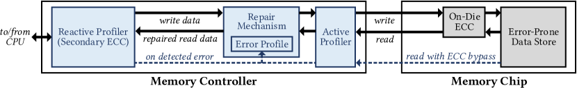
After active profiling is complete, the reactive profiler (i.e., a secondary ECC code with correction capability at least as strong as that of on-die ECC) continuously monitors for bits at risk of indirect errors. The reactive profiler is responsible only for identifying bits at risk of indirect errors the first time that they fail. If and when the reactive profiler identifies an indirect error, the location of the error is recorded to the error profile for subsequent repair.
7.5.2 Active Profiling Implementation
The active profiler follows the general round-based algorithm employed by state-of-the-art error profilers, as discussed in section 7.1. Each round of testing first programs memory cells with a standard memory data pattern that is designed to maximize the chance of observing errors (e.g., , , random data) [12, 414, 369, 283, 297]. Patterns may or may not change across testing rounds depending on the requirements of the particular data pattern. Once sufficiently many rounds are complete, the set of at-risk bits identified comprises the union of all bits identified across all testing rounds.
We assume that the active profiler achieves full coverage of bits at risk of direct errors by leveraging any or all of the worst-case testing techniques developed throughout prior works [468, 283, 285, 415, 414]. This is feasible because the active profiler can read and write to the raw data bits exploiting the ECC bypass path and the systematically-encoded data bits, respectively. Therefore, the active profiler can use techniques developed for memory chips without on-die ECC.
7.5.3 Reactive Profiling Implementation
HARP requires that the secondary ECC have correction capability at least as high as the number of indirect errors that on-die ECC can cause at one time. This requires the layout of secondary ECC words to account for the layout of on-die ECC words: the two must combine in such a way that every on-die ECC word is protected with the necessary correction capability by the secondary ECC. For example, with a single-error correcting on-die ECC that uses 128-bit words, the memory controller must ensure that every 128-bit on-die ECC word is protected with at least single-error correction.
How this is achieved depends heavily on a given system’s memory architecture. For example, depending on the size of an on-die ECC word and how many memory chips the memory controller interfaces with, on-die ECC words may be split across different data transfers. In this case, the system designer must choose a design that matches their design goals, e.g., dividing secondary ECC words across multiple transfers (which introduces its own reliability challenges [177]), or interleaving secondary ECC words across multiple on-die ECC words (which could require stronger secondary ECC).
Without loss of generality, we assume that the memory controller interfaces with a single memory chip at a time (e.g., similar to some LPDDR4 systems [250]) and provisions a single-error correcting code per on-die ECC word. Such a system is sufficient for demonstrating the error profiling challenges that we address in this work. Matching the granularity of secondary and on-die ECC words for arbitrary systems is not a problem unique to our work since any secondary ECC that is designed to account for the effects of on-die ECC must consider how the two interact [88, 177]. Therefore, we leave a general exploration of the tradeoffs involved to future work.
HARP-U and HARP-A.
We introduce two variants of HARP: HARP-A and HARP-U, which are aware and unaware of the on-die ECC parity-check matrix , respectively. HARP-A uses this knowledge to precompute777Using the methods described in detail in prior work [466]. bits at risk of indirect error given the bits at risk of direct error that are identified during active profiling. HARP-A does not provide benefits over HARP-U during active profiling. However, HARP-A reduces the number of bits at risk of indirect error that remain to be identified by reactive profiling.
Increasing the Secondary ECC Strength.
The secondary ECC is used for reactive profiling and must provide equal or greater correction capability than on-die ECC to safely identify indirect errors. Current on-die ECC designs are limited to simple single-error correcting codes due to area, energy, and latency constraints within the memory die [405, 177, 538], so the secondary ECC can be correspondingly simple. However, if either (1) future on-die ECC designs become significantly more complex; or (2) the system designer wishes to address other failure modes (e.g., component-level failures) using the secondary ECC, the system designer will need to increase the secondary ECC strength accordingly. Whether profile-based repair remains a feasible error-mitigation strategy in this case is ultimately up to the system designer and their reliability goals, so we leave further exploration to future work.
7.5.4 Limitations
HARP relies on the active profiler to achieve full coverage of bits at risk of direct errors so that the reactive profiler never observes a direct error (i.e., the reactive profiler’s correction capability is never exceeded). Consequently, if the active profiler fails to achieve full coverage, the reactive profiler may experience indirect errors in addition to direct error(s) missed by active profiling.
We acknowledge this as a theoretical limitation of HARP, but we do not believe it restricts HARP’s potential impact to future designs and scientific studies. This is because achieving full coverage of at-risk bits without on-die ECC is a long-standing problem that is complementary to our work. Prior works have studied this problem in detail [282, 285, 480, 468], and any solution developed for chips without on-die ECC can be immediately applied to HARP’s active profiling phase, effectively reducing the difficulty of profiling chips with on-die ECC to that of chips without on-die ECC.
7.6 Evaluations
In this section, we study how HARP’s coverage of direct and indirect errors changes with different pre-correction error counts and per-bit error probabilities to both (1) demonstrate the effect of the three profiling challenges introduced by on-die ECC and (2) show that HARP overcomes the three challenges.
7.6.1 Evaluation Methodology
We evaluate error coverage in simulation because, unlike with a real device, we can accurately compute error coverage using precise knowledge of which errors are and are not possible. This section describes our simulation methodology.
Baselines for Comparison.
We compare HARP-U and HARP-A with two baseline profiling algorithms that use multiple rounds of testing with different data patterns to identify at-risk bits based only on observing post-correction errors.
- 1.
-
2.
BEEP, the profiling algorithm supported by the reverse-engineering methodology BEER [466]. BEEP carefully constructs data patterns intended to systematically expose post-correction errors based on having reverse-engineered the on-die ECC parity-check matrix. We follow the SAT-solver-based methodology as described by [466] and use a random data pattern before the first post-correction error is confirmed.
Simulation Strategy.
We extend the open-source DRAM on-die ECC analysis infrastructure released by prior work [1, 466] to perform Monte-Carlo simulations of DRAM data retention errors. We release our simulation tools on Zenodo [469] and Github [5]. We simulate error injection and correction using single-error correcting Hamming codes [193] representative of those used in DRAM on-die ECC (i.e., (71, 64) [229, 435] and (136, 128) [447, 331, 330, 405] code configurations). All presented data is shown for a (71, 64) code, and we verified that our observations hold for longer (136, 128) codes. We simulate 1,036,980 total ECC words across 2769 randomly-generated parity-check matrices over 20 days of simulation time. For each profiler configuration, we simulate 128 profiling rounds because this is enough to understand the behavior of each configuration (e.g., the shapes of each curve in Fig. 7.4), striking a good balance with simulation time.
We inject errors according to the model discussed in section 7.2.2 to simulate the effect of uniform-random, data-dependent errors. We assume that all bits are true-cells [327, 369] that experience errors only when programmed with data ‘1’, which is consistent with experimental observations made by prior work [327, 466]. To study how varying error rates impact profiling, we simulate bit errors with Bernoulli probabilities of 1.0, 0.75, 0.5, and 0.25 and separate our results based on the total number of pre-correction errors injected into a given ECC word. Using this approach, one can easily determine the effect of an arbitrary raw bit error rate by summing over the individual per-bit error probabilities.
We define coverage as the proportion of all at-risk bits that are identified. We calculate coverage using the Z3 SAT solver [126], computing the total number of post-correction errors that are possible for a given (1) parity-check matrix; (2) set of pre-correction errors; and (3) (possibly empty) set of already-discovered post-correction errors. Note that a straightforward computation of coverage given on-die ECC is extremely difficult for data-dependent errors: each data pattern programs the parity-check bits differently, thereby provoking different pre-correction error patterns. Therefore, using the SAT solver, we accurately measure the bit error rate of all possible at-risk bits across all possible data patterns.
We simulate three different data patterns to exercise data-dependent behavior: random, charged (i.e., all bits are ‘1’s), and checkered (i.e., consecutive bits alternate between ‘0’ and ‘1’). For the random and checkered data patterns, we invert the data pattern each round of profiling. For the random pattern, we change the random pattern after every two profiling rounds (i.e., after both the pattern and its inverse are tested). We ensure that each profiler is evaluated with the exact same set of ECC words, pre-correction error patterns, and data patterns in order to preserve fairness when comparing coverage values. Unless otherwise stated, all data presented uses the random pattern, which we find performs on par or better than the static charged and checkered patterns that do not explore different pre-correction error combinations.
7.6.2 Active Phase Evaluation
We study the number of profiling rounds required by each profiling algorithm to achieve coverage of direct errors. We omit HARP-A because its coverage of direct errors is equal to that of HARP-U.
Direct Error Coverage.
Fig. 7.4 shows the coverage of bits at risk of direct errors that each profiler cumulatively achieves (y-axis) over 128 profiling rounds (x-axis) assuming four different values of pre-correction errors per ECC word (2, 3, 4, and 5). We report results for four different per-bit error probabilities of the injected pre-correction errors (25%, 50%, 75%, 100%). For each data point, we compute coverage as the proportion of at-risk bits identified out of all at-risk bits across all simulated ECC words.
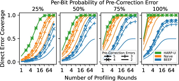
We make two observations. First, HARP consistently and quickly achieves full coverage, regardless of the number or per-bit error probabilities of the injected pre-correction errors. This is because HARP bypasses on-die ECC correction, identifying each at-risk bit independently, regardless of which error occurs in which testing round. In contrast, both Naive and BEEP (1) require more testing rounds to achieve coverage parity with HARP and (2) exhibit significant dependence on the number of pre-correction errors. This is a direct result of on-die ECC: each post-correction error depends on particular combination(s) of pre-correction errors, and achieving high coverage requires these combinations to occur in distinct testing rounds. We conclude that that HARP effectively overcomes the first profiling challenge by directly observing pre-correction errors, while Naive and BEEP must both rely on uncorrectable error patterns to incrementally improve coverage in each round.
Second, although, HARP and Naive both eventually achieve full coverage, BEEP fails to do so in certain cases. This is because BEEP does not explore all pre-correction error combinations necessary to expose each bit at risk of direct errors. We attribute this behavior to a nuance of the BEEP algorithm: BEEP crafts data patterns that increase the likelihood of indirect errors. Unfortunately, these patterns are slow to explore different combinations of pre-correction errors, which leads to incomplete coverage. This is consistent with prior work [466], which finds that BEEP exhibits low coverage when pre-correction errors are sparse or occur with low probability. We find that Naive also fails to achieve full coverage when using static data patterns (e.g., checkered) for the same reason.
Bootstrapping Analysis.
Fig. 7.5 shows the distribution (median marked with a horizontal line) of the number of profiling rounds required for each profiler to observe at least one direct error in each ECC word. If no post-correction errors are identified, we conservatively plot the data point as requiring 128 rounds, which is the maximum number of rounds evaluated (discussed in section 7.6.1). The data illustrates the difficulty of bootstrapping because observing any post-correction error with on-die ECC requires a specific combination of pre-correction errors to occur.
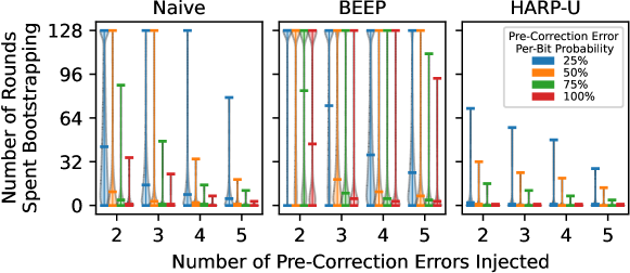
We make three observations. First, we see that HARP identifies the first error far more quickly than Naive or BEEP profiling across all configurations. Second, HARP never fails to identify at least one error within 128 rounds. Third, in contrast, BEEP sometimes cannot identify an error at all due to a combination of (1) the low per-bit pre-correction error probability and (2) the bootstrapping problem (i.e., more testing rounds does not guarantee higher coverage unless those rounds explore different uncorrectable patterns). We conclude that HARP effectively addresses the bootstrapping challenge by directly observing pre-correction errors instead of relying on exploring different uncorrectable error patterns.
7.6.3 Reactive Phase Evaluation
In this section, we study each error profiler’s coverage of bits at risk of indirect errors and examine the correction capability required from the secondary ECC to safely identify the at-risk bits remaining after active profiling. It is important to note that, unlike HARP, neither Naive nor BEEP profiling achieve full coverage of bits at risk of direct errors for all configurations. In such cases, multi-bit errors can occur during reactive profiling that are not safely identified by a single-error correcting code (studied in section 7.6.3), regardless of the profiler’s coverage of bits at risk of indirect errors.
Indirect Error Coverage.
Fig. 7.6 shows the proportion of all bits that are at risk of indirect errors that each profiler has missed per ECC word throughout 128 rounds of profiling. This is equivalent to the number of at-risk bits that reactive profiling has to identify. We evaluate an additional configuration, HARP-A+BEEP, which employs BEEP to identify the remaining at-risk bits once HARP-A has identified all bits at risk of direct errors.

We make three observations. First, HARP-U does not identify any bits at risk of indirect errors888Except for a small number of direct and indirect errors that overlap. because it bypasses the on-die ECC correction process that causes indirect errors. In contrast, HARP-A quickly identifies a subset of all bits at risk of indirect errors by predicting them from the identified direct errors. Note that HARP-A cannot identify all bits at risk of indirect errors because doing so would require knowing which parity-check bits are at risk of error, which the on-die ECC bypass path does not reveal.
Second, combining HARP-A with BEEP effectively overcomes HARP-A’s inability to identify pre-correction errors within the parity-check bits. This is because HARP-A+BEEP synergistically combines (1) HARP’s ability to quickly identify bits at risk of direct errors with (2) BEEP’s ability to exploit known at-risk bits to expose others. The combined configuration quickly identifies bits at risk of indirect errors, achieving coverage similar to Naive and BEEP profiling in less than half the number of profiling rounds.
Third, both Naive and BEEP achieve relatively high coverage of indirect errors after many (i.e., ) rounds compared to HARP-U and HARP-A. This is because both Naive and BEEP continually explore different uncorrectable error patterns, steadily exposing more and more indirect errors. BEEP achieves higher coverage because its algorithm deliberately seeks out pre-correction error combinations that are more likely to cause post-correction errors, thereby exposing more indirect errors in the long run.
We conclude that knowing the on-die ECC parity-check matrix helps HARP-A and BEEP identify bits at risk of indirect errors, thereby reducing the number of indirect errors that must be identified by by the secondary ECC during reactive profiling.
Secondary ECC Correction Capability.
Fig. 7.7 shows the worst-case (i.e., maximum) number of post-correction errors that can occur simultaneously within an ECC word after active profiling. This number is the correction capability required from secondary ECC to safely perform reactive profiling.
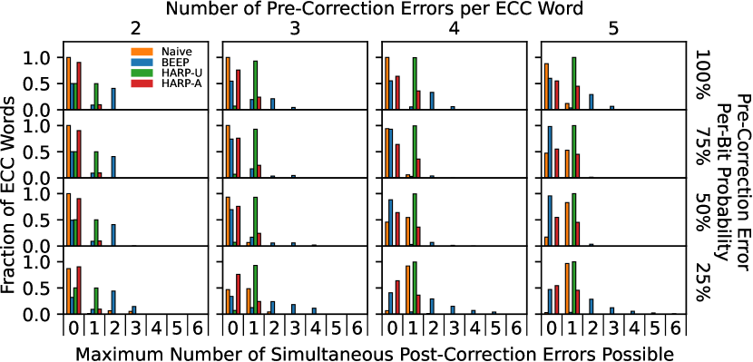
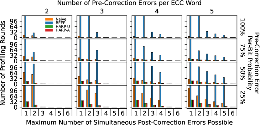
Maximum Error Count. Fig. 7.7a shows a normalized histogram of the maximum number of post-correction errors that can occur simultaneously within each simulated ECC word given all at-risk bits missed after 128 rounds of active profiling. We observe that both HARP-U and HARP-A exhibit at most one post-correction error across all configurations. This is because HARP identifies all bits at risk of direct errors within 128 profiling rounds (shown in Fig. 7.4), so only one error may occur at a time (i.e., an indirect error). In contrast, both Naive and BEEP are susceptible to multi-bit errors. In particular, BEEP’s relatively low coverage of bits at risk of direct errors means that many multi-bit error patterns remain possible. We conclude that, after 128 rounds of active profiling, a single-error correcting secondary ECC is sufficient to perform reactive profiling for HARP but insufficient to do so for Naive and BEEP.
Maximum Error Count. Fig. 7.7b shows how many active profiling rounds are required to ensure that no more than an x-axis value of post-correction errors can occur simultaneously in a single ECC word during reactive profiling. We conservatively report results for the 99th percentile of all simulated ECC words because neither Naive nor BEEP achieve full coverage of bits at risk of direct errors for all configurations within 128 profiling rounds. In cases where 128 profiling rounds are insufficient to achieve 99th-percentile values, we align the bar with the top of the plot.
We make two observations. First, both HARP configurations perform significantly faster than Naive and BEEP. For example, with a 50% pre-correction per-bit error probability, HARP ensures that no more than one post correction error can occur in 20.6%/36.4%/52.9%/62.1% of the profiling rounds required by Naive given 2/3/4/5 pre-correction errors. This is because HARP quickly identifies all bits at risk of direct errors, while Naive and BEEP both either (1) take longer to do so; or (2) fail to do so altogether (e.g., for the 100th percentile at a 50% per-bit error probability). Second, BEEP performs much worse than any other profiler because it exhibits extremely low coverage of bits at risk of direct error (studied in section 7.6.2). We conclude that achieving high coverage of bits at risk of direct errors is essential for minimizing the correction capability of the secondary ECC.
7.6.4 Case Study: DRAM Data Retention
In this section, we show how error profiling impacts end-to-end reliability. We study the bit error rate of a system that uses a bit-granularity repair mechanism (e.g., such as those discussed in section 2.3.4) to reduce the DRAM refresh rate, which prior work shows can significantly improve overall system performance and energy-efficiency [571, 370, 480, 468] and enable continued density scaling [434]. We assume that data-retention errors follow the error model described in section 7.2.2 (i.e., uniformly with a fixed raw bit error rate, which is consistent with prior experimental studies [546, 468, 37, 191, 295, 526, 467]) and that the repair mechanism perfectly repairs any at-risk bits that are identified by either active or reactive profiling. We assume a (71, 64) SEC on-die ECC code and a secondary ECC capable of detecting and correcting a single error in each on-die ECC word during reactive profiling.
Fig. 7.8 illustrates the fraction of all bits that are at risk of post-correction errors (i.e., the bit error rate) before (Fig. 7.8, left) and after (Fig. 7.8, right) secondary ECC is applied (i.e., before and after performing reactive profiling) given an x-axis number of active profiling rounds. Each line marker shows a different data-retention RBER (e.g., due to operating at different refresh rates).
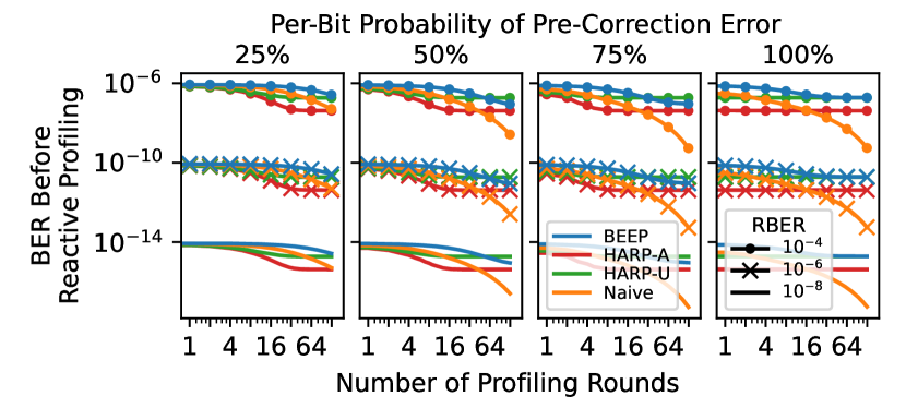
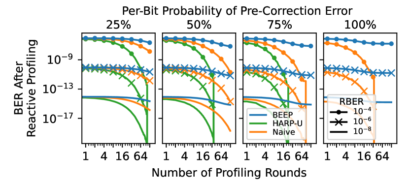
We make three observations. First, all profilers in Fig. 7.8 (left) behave consistently with the coverage analysis of section 7.6.2. HARP quickly identifies all bits at risk of direct error, but leaves indirect errors to be identified by reactive profiling. Both Naive and BEEP slowly explore different combinations of pre-correction errors, with Naive steadily reducing the BER given more profiling rounds while BEEP fails to do so.
Second, Fig. 7.8 (left) shows the benefit of HARP-A knowing the on-die ECC function. While both HARP-U and HARP-A quickly identify all bits at risk of direct errors, HARP-A also identifies bits at risk of indirect errors, thereby considerably reducing the overall BER (and therefore, the total number of bits) that remain to be identified by reactive profiling.
Third, Fig. 7.8 (right) shows that both HARP999HARP-A is not shown in Fig. 7.8 (right) because it exhibits identical BER to HARP-U after applying secondary ECC (i.e., because both profilers have identical coverage of bits at risk of direct errors). and Naive reach a BER of zero after sufficiently many profiling rounds, though Naive takes significantly more profiling rounds to do so (e.g., for a per-bit pre-correction error probability of 75%). This behavior is consistent with the fact that both profilers eventually achieve full coverage of bits at risk of direct error (shown in section 7.6.2) In contrast, BEEP fails to reach a zero probability value because it fails to achieve full coverage of bits at risk of direct error. Note that HARP-U immediately identifies all bits at risk of direct errors in the first profiling round with a per-bit pre-correction error probability of 100%, so it is not visible in the rightmost plot.
We conclude that HARP effectively identifies all bits at-risk of error faster than the baseline profilers, thereby enabling the repair mechanism to safely operate at the evaluated raw bit error rates. Although this case study uses a simple data-retention error model that does not include low-probability errors or other failure modes (discussed in section 7.2.2), it demonstrates (1) the importance of a practical and effective error profiling algorithm in enabling a repair mechanism to mitigate errors; and (2) the advantages that HARP provides in an end-to-end setting by overcoming the error profiling challenges introduced by on-die ECC.
7.7 Summary
We study how on-die ECC affects memory error profiling and identify three key challenges that it introduces: on-die ECC (1) exponentially increases the number of at-risk bits the profiler must identify; (2) makes individual at-risk bits more difficult to identify; and (3) interferes with commonly-used memory data patterns. To overcome these three challenges, we introduce Hybrid Active-Reactive Profiling (HARP), a new bit-granularity error profiling algorithm that enables practical and effective error profiling for memory chips that use on-die ECC. HARP exploits the key idea that on-die ECC introduces two different sources of post-correction errors: (1) direct errors that result from pre-correction errors within the data portion of the ECC codeword; and (2) indirect errors that are a result of the on-die ECC correction process. If all bits at risk of direct error are identified, the number of concurrent indirect errors is upper-bounded by the correction capability of on-die ECC. Therefore, HARP uses simple modifications to the on-die ECC mechanism to quickly identify bits at risk of direct errors and relies on a secondary ECC within the memory controller to safely identify indirect errors. Our evaluations show that HARP achieves full coverage of all at-risk bits in memory chips that use on-die ECC faster than prior approaches to error profiling. We hope that the studies, analyses, and ideas we provide in this work will enable researchers and practitioners alike to think about and overcome the challenge of how to handle error detection and correction across the hardware-software stack in the presence of on-die ECC.
?chaptername? 8 A Case for Transparent Reliability in DRAM Systems
The previous four chapters closely studied new challenges that on-die ECC introduces because of the way that it obfuscates memory errors in the context of error profiling, error characterization, and error mitigation. In this chapter, based on the understanding and technical contributions we developed so far, we argue for the importance of having transparency into basic commodity DRAM reliability characteristics. We then introduce our recommendations to facilitate such transparency in current and future commodity DRAM-based systems.
8.1 Background and Motivation
Dynamic Random Access Memory (DRAM) [132, 133, 279, 387, 439, 9] is the dominant choice for main memory across a broad range of computing systems because of its high capacity at low cost relative to other viable main memory technologies. Building efficient DRAM chips requires substantially different manufacturing processes relative to standard CMOS fabrication [317], so DRAM is typically designed and manufactured separately from other system components. In this way, system designers who purchase, test, and/or integrate commodity DRAM chips (e.g., cloud system designers, processor and system-on-a-chip (SoC) architects, memory module designers, test and validation engineers) are free to focus on the particular challenges of the systems they work on instead of dealing with the nuances of building low-cost, high-performance DRAM.
To ensure that system designers can integrate commodity DRAM chips from any manufacturer, the DRAM interface and operating characteristics have long been standardized by the JEDEC consortium [244]. JEDEC maintains a limited set of DRAM standards for commodity DRAM chips with different target applications, e.g., general-purpose DDRn [246, 249, 253], bandwidth-optimized HBMn [256, 257], mobile-oriented LPDDRn [250, 254], graphics-oriented GDDRn [251, 255]. Given that DRAM designs are heavily constrained by DRAM standards, manufacturers generally seek profitability through economies of scale [274, 129, 352, 120]: they mass produce standards-compliant DRAM chips using highly-optimized manufacturing processes. High-volume production amortizes manufacturing costs and increases per-chip profit margins. As such, DRAM manufacturers conservatively regard design- and manufacturing-related information as sensitive [434, 176, 105, 224], revealing only what DRAM standards require.
To maintain their competitive advantage in cost-per-capacity, DRAM manufacturers continually improve storage densities across successive product generations while minimizing fabrication costs (e.g., minimizing chip area, maximizing yield). This requires a careful balance between aggressively scaling physical feature sizes, continually optimizing circuit designs to reduce area consumption, and mitigating reliability issues that arise with process technology shrinkage [276, 88, 434, 405, 461, 538, 10]. Unfortunately, focusing primarily on storage density forces DRAM manufacturers to sacrifice potential improvements in other metrics of interest, such as performance, energy, etc. Even if process technology shrinkage naturally provides gains in these other metrics (e.g., by reducing circuit latencies with smaller circuit elements), manufacturers typically adjust their designs to exchange these gains for additional storage density (e.g., by building larger array sizes that offset any reductions in access latency). As manufacturers juggle the complex tradeoffs in chip design and manufacturing to maintain market competitiveness, DRAM as a whole exhibits slow generational improvements in key areas, such as access latency and power consumption [90, 344, 164].
Figure 2 provides a best-effort survey showing how manufacturer-reported values for four key DRAM operating timings and per-chip storage capacity (all shown in log scale) have evolved over time. We extract these data values from 58 publicly-available DRAM chip datasheets from across 19 different DRAM manufacturers with datasheet publication dates between 1970 and 2021. This data encompasses DRAM chips from both asynchronous (e.g., page mode, extended data out) and synchronous (e.g., SDRAM, DDRn) DRAM chips. Appendix LABEL:position:appendix_a describes our data collection methodology in further detail, and Appendix 8.B provides an overview of our dataset, which is publicly available on GitHub [2].
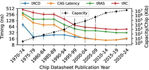
Parameter Definition tRCD minimum row activation to column operation delay CAS Latency read operation to data access latency tRAS minimum row activation to precharge delay tRC minimum delay between accesses to different rows across each 5-year period of time.
8.1.1 Motivation: The Need for Adaptability
We observe a clear trend that newer DRAM chips exhibit improvements in all four timing parameters and storage capacity. However, none of the four timings have improved significantly in the last two decades. For example, the median tRCD/CAS Latency/tRAS/tRC reduced by 2.66/3.11/2.89/2.89% per year on average between 1970 and 2000, but only 0.81/0.97/1.33/1.53% between 2000 and 2015.333We report 2015 instead of 2020 because 2020 shows a regression in CAS latency due to first-generation DDR5 chips, which we believe is not representative because of its immature technology. In contrast, storage capacity improved relatively consistently with an exponential growth factor of 0.328 per year (0.341 for 1970-2000 and 0.278 for 2000-2020) across the entire history of DRAM technology. This data is consistent with similar studies done in prior work [539, 90, 347, 202, 91, 344, 232, 108, 62, 443], showing that commodity DRAM manufacturers have prioritized storage capacity over access latency in recent years.
Unfortunately, prioritizing storage density does not always align with the increasingly diverse needs of modern computing systems. These needs change as systems continuously evolve, so there is no single target metric (e.g., storage capacity) that suits all DRAM-based systems. Instead, each system’s design goals differ based on factors such as cost, complexity, applications, etc. For example, storage-focused data centers (e.g., content delivery network nodes) may require high-reliability memory while compute-focused clusters may optimize for performance with low-latency memory. Unfortunately, system designers today are limited to a narrow range of commodity DRAM products,444Custom DRAM chips (e.g., latency-optimized [403, 156], high-reliability [534, 229]) and target-specific chips (e.g., LPDDRn [250, 254], GDDRn [251, 255]) sacrifice the cost advantages of high-volume general-purpose commodity DRAM [352]. that effectively restrict design freedom and limit the peak potential of DRAM-based systems.
To address this disparity, system designers have long since developed techniques for adapting unmodified commodity DRAM chips to varying system requirements. Examples include: (1) actively identifying and/or mitigating errors to improve reliability [301, 86, 614, 563, 260, 302, 435, 261, 194, 98, 102, 385, 470, 107, 523, 23, 430, 33]; (2) exploiting available timing [89, 91, 294, 343, 346, 586, 627, 326] and voltage [94, 125, 131] margins to reduce memory access latency, power consumption, decrease refresh overheads [571, 370, 434, 468, 366, 165, 584, 480, 468]; and (3) mitigating unwanted DRAM data persistence [189, 182, 530] and read-disturb problems [605, 312, 30, 307, 497]. Section 8.2.1 discusses these proposals in greater detail to motivate the need to adapt commodity DRAM to diverse yet aggressive design targets.
However, these proposals are largely theoretical ideas or proofs-of-concept based on performance and reliability characteristics that are assumed, inferred, or reverse-engineered from a limited set of observations and DRAM products (e.g., in-house experimental studies) without DRAM manufacturers’ support. Therefore, adopting such proposals in a consumer-facing product requires a system designer to weigh the benefits of enhancing DRAM (e.g., improving performance, security, etc.) against both: (1) risks (e.g., failures in the field) associated with potentially violating manufacturer-recommended operating conditions and (2) limitations due to compatibility with only a subset of all commodity DRAM products (e.g., only those that have been accurately reverse-engineered). These risks and limitations are a serious barrier to adoption, especially for small-scale designers who may have limited headroom and expertise for exploring unconventional designs.
In this work, we argue that the lack of transparency concerning DRAM reliability characteristics is ultimately responsible for confining system designers to conventional, specification-constrained designs. For example, safely improving DRAM access latency by adjusting operating timings requires understanding the possible failure modes resulting from using non-standard timings (discussed further in Section 8.6). This is because selecting suitable operating timings requires the system designer to estimate the reliability impact of the new timings, which in turn requires reliability modeling or extensive testing under worst-case operating conditions. Unfortunately, obtaining the information necessary to make these estimates (e.g., error models, worst-case testing parameters) is difficult, if not impossible,555For all but the largest customers capable of independently conducting rigorous post-manufacturing testing. without transparency from DRAM manufacturers. This transparency does not exist today, even through private agreements for high-volume consumers who have significant stake in the DRAM industry [8, 504, 374]. In general, without the ability to understand how different design choices can impact DRAM reliability (e.g., error rates), system designers are discouraged from deploying or even exploring alternative designs.
To understand the source of the transparency problem, we conduct four case studies throughout Sections 8.4–8.7 that each examine a key system design concern for commodity DRAM chips: (1) reliability; (2) refresh overheads; (3) access latency; and (4) the RowHammer security vulnerability. For each case study, we explain how system designers are forced to make assumptions about DRAM reliability in order to address these concerns without breaking design independence with DRAM manufacturers, but those very assumptions limit the practicality and scope of the solution. We then argue that DRAM standards lie at the heart of the problem because they do not adequately address the aforementioned DRAM reliability concerns. To overcome this reliance on assumptions, we show that incorporating specifications for consumer-visible DRAM reliability characteristics (e.g., industry-validated error models and testing techniques) into DRAM standards alleviates the problem and allows system designers to better adapt commodity DRAM to their particular needs without requiring changes to how DRAM manufacturers design and build commodity DRAM.
We propose incorporating information transparency into DRAM standards using a two-step approach involving all DRAM stakeholders, including consumers and manufacturers. In Step 1, for DRAM chips already in the field, we seek the release of basic information about DRAM chips that consumers can use to better understand the chips’ reliability characteristics. Section 8.9.1 details examples of possible information to release, including (1) basic microarchitectural characteristics (e.g., organization of physical rows, sizes of internal storage arrays) that can be reverse-engineered using existing techniques with access to appropriate testing infrastructure [267, 343, 467, 91, 415, 295, 327, 294, 455, 198] and (2) industry-recommended testing best practices (e.g., test patterns for key error mechanisms). We believe that this information can be released through a combination of (1) crowdsourced testing of commodity DRAM chips on the market; and (2) DRAM chip manufacturers publishing information (e.g., using datasheet revisions or online resources) about their products, possibly limited to basic information that manufacturers already have available (i.e., that requires minimal logistical effort to release). Through a combination of these two avenues, information can be provided to all system designers, including the majority of designers without the ability to conduct exhaustive testing, almost immediately without requiring changes to existing DRAM hardware or standards (though standardizing the information release could streamline the process). Then, armed with this information, system designers can make more informed decisions when developing their own solutions to system-specific design concerns while also preserving the advantages of commodity DRAM built per general-purpose DRAM standards.
In Step 2, we propose extending DRAM standards with explicit DRAM reliability standards that provide industry-standard guarantees, tools, and/or information helpful to consumers. We envision different possibilities for these reliability standards, including (1) reliability guarantees for how a chip is expected to behave under certain operating conditions (e.g., predictable behavior of faults [119]); (2) disclosure of industry-validated DRAM reliability models and testing strategies suitable for commodity DRAM chips (e.g., similar to how JEDEC JEP122 [252], JESD218 [247], and JESD219 [248] address Flash-memory-specific error mechanisms [74, 78, 75] such as floating-gate data retention [81, 379, 380, 83] and models for physical phenomena such as threshold voltage distributions [79, 82, 80, 378]); and (3) requirements for manufacturers to directly provide relevant information about their DRAM chips (e.g., the information requested in Step 1). As the DRAM industry continues to evolve, we anticipate closer collaboration between DRAM and system designers to efficiently overcome the technology scaling challenges that DRAM is already facing [276, 405, 420, 421]. Although we hope that transparency will occur naturally as part of this process, we believe the end result will be determined in a large part by the direction in which DRAM standards evolve. Therefore, we believe that ensuring transparency of reliability characteristics becomes a first-order concern is essential for allowing innovation going forward.
8.2 The System Designer’s Challenge
Today’s DRAM industry thrives on separation of concerns: DRAM manufacturers can focus on designing highly-optimized DRAM chips while consumers can make use of standardized DRAM that conform to JEDEC standards. This design independence is powerful because it allows each party to leverage their respective expertise to build the best possible product. As a result, a system designer who is responsible for choosing the memory substrate for a particular system can simply select between a limited range of standardized commodity parts that are optimized for different targets, such as general-purpose performance (e.g., DDRn [249, 253]), high bandwidth (e.g., GDDRn [251, 255], HBMn [256, 257]), and low power (e.g., LPDDRn [250, 254]).
Unfortunately, the system designer faces a significant challenge: the designer is unable to fully explore the memory design space (as well as the system-memory co-design space) because there are only a limited number of viable design points using commodity DRAM chips. Therefore, the limited number of options inherently forces the designer to overlook opportunities for customizing DRAM operation towards their system’s particular design goals. As main memory becomes an increasingly significant system bottleneck [420, 429, 424], we believe that enabling system designers to flexibly adapt commodity DRAM to suit their own needs as they see fit is a promising path to reap the benefits of adaptability while preserving the design independence between DRAM manufacturers and system designers.
8.2.1 Benefits for DRAM Consumers
Prior works [301, 86, 614, 563, 260, 302, 435, 261, 98, 102, 385, 470, 584, 393, 446, 571, 37, 220, 397, 370, 449, 582, 366, 434, 165, 480, 282, 284, 283, 285, 241, 298, 300, 278, 468, 390, 89, 91, 294, 343, 346, 586, 627, 197, 326, 390, 620, 159, 295, 451, 452, 296, 514, 513, 516, 518, 187, 515, 605, 181, 423, 312, 325, 567, 71, 497] demonstrate significant system-level benefits from adapting commodity DRAM operation to different system needs without changing the DRAM design itself. This section reviews the benefits of four concrete examples of such customizations: 1) DRAM reliability improvement, 2) DRAM refresh overhead reduction, 3) DRAM access latency reduction, and 4) RowHammer security improvement. In principle, a system designer can readily implement each customization using existing techniques. Unfortunately, adopting these techniques in practice requires understanding how DRAM reliability characteristics behave under different operating conditions, which is not clearly communicated by DRAM manufacturers or standards today. In this section, we review each example customization’s potential benefits; then, our case studies throughout Sections 8.4-8.7 explore each example customization in further detail to identify the specific factors that we believe discourage system designers from adopting the examples in practice.
DRAM Reliability Improvement
DRAM is susceptible to a wide variety of error mechanisms that can impact overall system reliability. To combat DRAM-related failures, system designers typically incorporate reliability, availability and serviceability (RAS) features [547, 130, 532] that collectively improve system reliability beyond what commodity DRAM chips can provide alone. In general, memory RAS is a broad research area with solutions spanning the hardware-software stack, ranging from hardware-based mechanisms within the DRAM chip (e.g., on-die ECC scrubbing [253, 484, 119], post-package repair [212, 249, 253, 287, 575], target row refresh [198, 154]), memory controller (e.g., rank-level ECC [301, 86, 614, 563, 260, 302, 435, 261, 98, 102, 385, 470, 584], rank-level ECC scrubbing [194, 480, 107, 523, 23, 430, 33, 540, 484, 523], repair techniques [366, 434, 321, 373, 320, 507, 432, 622, 581, 289]) to software-only solutions (e.g., page retirement [393, 446, 571, 37, 220, 397], failure prediction [416, 52, 167, 336, 363, 61]).
As a specific and relevant example, an important category of hardware-based redundancy mechanisms known as rank-level error-correcting codes (rank-level ECC) operate within the memory controller to isolate the rest of the system from random DRAM errors. Depending on the ECC design, rank-level ECC can protect against random single-bit (e.g., SEC/SEC-DED Hamming codes [193]), multi-bit (e.g., BCH [210, 69], Reed-Solomon [489]), and/or multi-component (e.g., Chipkill [129, 301]) errors with varying hardware and runtime overheads. The system designer must decide which ECC mechanism is most appropriate for their particular system (e.g., which error mechanisms are dominant and what degree of protection is required). For example, a state-of-the-art rank-level ECC mechanism called Frugal-ECC [302] uses data compression to provide chipkill-correct ECC for 4 non-ECC DIMMs and 8 ECC DIMMs with negligible performance (maximum of 3.8%), energy-efficiency, and area overheads compared with an industry-standard chipkill solution. Therefore, Frugal-ECC enables system designers to implement chipkill reliability using commodity DRAM chips with a fraction of the storage overheads suffered by conventional ECC DIMM configurations.
DRAM Refresh Overhead Reduction
DRAM stores data in volatile capacitors, which are susceptible to charge leakage. To prevent this leakage from causing data loss, DRAM requires periodic refresh operations that intermittently access all DRAM cells to restore their charge levels to safe values. Unfortunately, DRAM refresh operations are well known to waste significant system performance and power [449, 298, 338, 370, 434, 59, 582, 37, 390, 58], sacrificing almost half of the total memory throughput and wasting almost half of the total DRAM power for projected 64 Gb chips [370].
To alleviate the power and performance costs of DRAM refresh, prior works [370, 449, 582, 571, 366, 434, 165, 480, 282, 284, 283, 285, 241, 298, 300, 278, 468, 390] take advantage of the fact that most refresh operations are unnecessary.666Latency-hiding techniques (e.g, prefetching, memory command scheduling, on-chip caching, etc.) and parallelization of refresh and access operations [92, 443, 457, 544, 418] help mitigate performance overheads but do not change the total number of refresh operations issued. As a result, such techniques cannot mitigate energy wastage due to DRAM refresh. These techniques are also imperfect in many cases where latency-hiding is impractical (e.g., row conflicts between refresh and access commands, larger memory footprints than available caching resources) [431, 457, 624, 92]. The standard DRAM refresh algorithm refreshes all cells frequently (i.e., at the worst-case rate) to simplify DRAM refresh and guarantee correctness. However, each cell’s data retention characteristics vary significantly due to a combination of data-dependence [283, 285, 369, 282, 468] and process variation [190, 191, 176, 434, 369, 370, 582]. As a result, eliminating unnecessary refresh operations can provide significant power reduction and performance improvement. For example, Liu et al. [370] demonstrate an average energy-per-access and system performance improvement of 8.3% and 4.1%, respectively, for 4 Gib chips (49.7% and 107.9% for 64 Gib chips) when relaxing the refresh rate at the row granularity. Therefore, reducing refresh overheads can potentially benefit any DRAM-based system.
DRAM Access Latency Reduction
Figure 2 shows that DRAM access latency has not significantly improved relative to storage capacity over the last two decades. This makes DRAM an increasingly significant system performance bottleneck today, especially for workloads with large footprints that are sensitive to DRAM access latency [215, 148, 186, 203, 218, 633, 453, 65, 63, 326, 271, 539, 420, 595, 600, 427, 428, 272, 429, 57, 56, 372, 161, 525, 163]. Although conventional latency-hiding techniques (e.g., caching, prefetching, multithreading) can potentially help mitigate many of the performance concerns, these techniques (1) fundamentally do not change the latency of each memory access and (2) fail to work in many cases (e.g., irregular memory access patterns, random accesses, huge memory footprints).
To address this problem, prior works have taken two major directions. First, many works [89, 91, 294, 343, 346, 586, 627, 197, 326, 390, 620] show that the average DRAM access latency can be shortened by reducing DRAM access timings for particular memory locations that can tolerate faster accesses. This can be done safely because, although DRAM standards call for constant access timings across all memory locations, the minimum viable access timings that the hardware can support actually differ between memory locations due to factors such as heterogeneity in the circuit design [346, 344] and manufacturing process variation between circuit components [89, 91, 294, 94, 343].
Exploiting these variations in access timings to reduce the average memory access latency can provide significant system performance improvement. For example, Chang et al. [91] experimentally show that exploiting access latency variations can provide an average 8-core system performance improvement of 13.3%/17.6%/19.5% for real DRAM chips from three major DRAM manufacturers. Similarly, Kim et al. [294] show that exploiting access latency variations induced by DRAM sense amplifiers provides an average (maximum) system performance improvement of 4.97% (8.79%) versus using default DRAM access timings for 4-core heterogeneous workload mixes based on data obtained from 282 commodity LPDDR4 DRAM chips.
Second, other works [159, 295, 451, 452, 296, 514, 513, 516, 518, 187, 515] show that commodity DRAM can perform massively-parallel computations (e.g., at the granularity of an 8 KiB DRAM row) by exploiting the underlying analog behavior of DRAM operations (e.g., charge sharing between cells). These works show that such computations can significantly improve overall system performance and energy-efficiency by both (1) reducing the amount of data transferred between the processor and DRAM and (2) exploiting the relatively high throughput of row-granularity operations. For example, Gao et al. [159] show that in-DRAM 8-bit vector addition is more energy-efficient than the same computation in the processor, primarily due to avoiding the need for off-chip data transfers. Similarly, Olgun et al. [451] use an end-to-end FPGA-based evaluation infrastructure to demonstrate that in-DRAM copy and initialization techniques can improve the performance of system-level copy and initialization by and , respectively.
Improving Security Against RowHammer
RowHammer [312, 38, 422, 426] is a well-studied read-disturb phenomenon in modern DRAM chips in which memory accesses to a given memory location can induce bit-flips at other locations. Recent experimental studies [312, 297] show that RowHammer is continually worsening with process technology shrinkage. Although DRAM manufacturers incorporate internal RowHammer-mitigation mechanisms [127, 350, 154, 198, 115, 297, 407], prior work [154, 113, 198, 243, 127] shows that these mechanisms do not suffice. Therefore, several works [605, 462, 312, 603, 19, 30] provide RowHammer-mitigation mechanisms that operate from outside of the DRAM chip to provide strong security without requiring changes to DRAM chip hardware or relying upon information from DRAM manufacturers. Such a solution is attractive for a system designer with interest in building a secure system because the designer can rely upon their own methods rather than relying upon external, possibly difficult-to-verify promises or guarantees [504, 479].
Following prior work [605], we classify previously-proposed RowHammer defenses into four different categories as follows.
-
1.
Access-agnostic mitigation hardens a DRAM chip against RowHammer independently of the memory access pattern. This includes increasing the overall DRAM refresh rate [312, 30, 19] and memory-wide error correction and/or integrity-checking mechanisms such as strong ECC [479, 115, 312]. These mechanisms are algorithmically simple but can introduce significant system hardware, performance, and/or energy-efficiency overheads (e.g., a large number of additional refresh operations [312, 297, 58]).
- 2.
- 3.
- 4.
RowHammer defense is an ongoing area of research, and which mechanism type is most effective depends on the level of security (e.g., the threat model) that the system designer requires and the trade-offs (e.g., performance, energy, hardware area, complexity overheads) they are willing to make.
8.2.2 Benefits for DRAM Manufacturers
We believe that the ability to adapt commodity DRAM to system-specific design goals also benefits DRAM manufacturers for two key reasons. First, adaptability broadens the scope and competitive advantage of DRAM technology relative to alternative technologies (e.g., emerging memories). Second, enabling DRAM consumers to more easily innovate on the DRAM substrate can encourage valuable feedback for DRAM manufacturers, including insights from customer use-cases and well-evaluated suggestions for future products.
Regardless of these benefits, we believe making commodity DRAM adaptable has no significant downside for DRAM manufacturers. The reliability characteristics that we wish to be communicated (as described in detail in Section 8.9.1) are either (1) already exposed in scientific studies today; or (2) can be reverse-engineered using existing techniques by those with access to appropriate tools (e.g., competitors, scientific labs). We simply ask for these characteristics to be officially provided in a trustworthy capacity. DRAM manufacturers have not previously provided this information because there has been no pressing need to do so. However, releasing this information makes sense today because it can enable a broad range of benefits for DRAM consumers going forward, especially as DRAM technology scaling continues to face increasing difficulties [420, 425, 422].
8.2.3 Short-Term vs. Long-Term Solutions
Prior works [471, 429, 425, 420, 312, 276, 422, 426] have praised the merits of cooperation between DRAM manufacturers and system designers in order to collaboratively solve main memory challenges across the system stack. However, this requires either (1) breaking design independence between the two parties; (2) achieving consensus among all DRAM stakeholders (i.e., JEDEC committee members and representatives, including DRAM manufacturers and consumers) for every design change, followed by a lengthy adoption period; or (3) reducing dependence on DRAM standards and JEDEC. We do not believe any of these options are easy to adopt for either the (1) short term, where we would like to quickly effect changes that enable information transparency; or (2) long term, where breaking design independence constrains the very freedom that we advocate system designers should have in meeting their own design goals while preserving the cost advantages of mass-produced commodity DRAM chips.
Instead, we argue for enabling each party to solve their own system-specific design challenges, modifying DRAM standards only for issues that collectively affect all DRAM stakeholders. However, regardless of how the DRAM industry evolves over the coming years, we firmly believe that DRAM must become more adaptable, whether that occurs through standards or collaboration.
8.3 Quantitatively Measuring Reliability
As we will show in the following case studies (Sections 8.4–8.7), a system designer exploring unconventional DRAM operating points must first understand how reliably a chip will behave at that operating point. Given that this behavior is not governed by DRAM standards or described by DRAM manufacturers, the system designer must determine it themselves, e.g., through modeling and/or testing. This section formalizes the information that a system designer may need (but does not necessarily have access to today) in order to quantitatively understand DRAM reliability.
8.3.1 Information Flow During Testing
Figure 8.2 describes the flow of information necessary for a system designer to quantitatively estimate777“Estimate” because, in general, no model or experiment is likely to be perfect, including those provided by manufacturers. a DRAM chip’s error characteristics starting from basic properties of the chip . In principle, these characteristics can comprise any aspect of DRAM reliability that a system designer wants to quantify while exploring their system’s design and/or configuration space. Examples include: (1) worst-case error rates (e.g., bit error rate (BER) or failures in time (FIT)) across a given set of operating points; (2) a profile of error-prone memory locations; or (3) a list of error-free operating points (e.g., as identified in a shmoo analysis [46]). The error characteristics can be estimated in two different ways: testing or modeling.
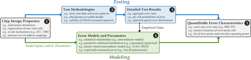
Determination from Testing
First, a system designer may estimate error characteristics using measurements from detailed experimental testing across a variety of operating conditions. Examples of measured quantities include: aggregate error rates, per-cell probabilities of error, and spatial/temporal error distributions. These measurements can be made using testing infrastructures ranging from industry-standard large-scale testing equipment [15, 560] to home-grown tools based on commodity FPGAs [199, 451, 213, 312, 159, 94, 164, 589, 91, 282, 580, 335] or DRAM-based computing systems [536, 113, 566, 153, 125].
To conduct accurate and rigorous testing, the system designer must use an effective test methodology that suits the particular DRAM chip under test. Prior works extensively study key aspects of effective test methodologies, including appropriate data and access patterns, the effects of enabling/disabling DRAM chip features such as target row refresh (TRR) [154, 386, 198, 243, 297] and on-die error correcting codes (on-die ECC) [435, 405, 276, 448, 176, 538, 447, 330, 332, 467, 466, 464], and the viability of different DRAM command sequences (e.g., sequences that enable in-DRAM row copy operations [514, 159, 451, 93], true random-number generation [452, 296, 550, 70], and physically unclonable functions [295, 551]).
In turn, choosing an effective test methodology requires knowledge of basic properties about a DRAM chip’s design and/or error mechanisms . For example, DRAM manufacturer’s design choices for the sizes of internal storage arrays (i.e., mats [346, 623, 539, 452]), charge encoding conventions of each cell (i.e., the true- and anti-cell organization [327, 369]), use of on-die reliability-improving mechanisms (e.g., on-die ECC, TRR), and organization of row and column addresses all play key roles in determining if and how susceptible a DRAM chip is to key error mechanisms (e.g., data retention [191, 327, 467, 369, 35, 588, 607], access-latency-related failures [294, 347, 343, 346, 91, 452, 326, 89], and RowHammer [312, 422, 426, 576, 611, 460]). Section 8.9.1 provides further detail about such design properties and how knowing them is necessary to develop effective test methodologies.
Determination from Modeling
Second, the system designer may make predictions from analytical or empirical error models based on a previous understanding of DRAM errors (e.g., from past experiments or scientific studies). Examples of such error models include: analytical models based on understanding DRAM failure modes (e.g., sources of runtime faults [120, 123, 86, 220, 529, 398]), parametric statistical models that provide useful summary statistics (e.g., lognormal distribution of cell data-retention times [190, 191, 264, 207, 362, 208, 141, 305, 323], exponential distribution of the time-in-state of cells susceptible to variable-retention time (VRT) [35, 286, 480, 608, 491, 526, 290, 291, 329, 410, 450, 282, 276, 369]), physics-based simulation models (e.g., TCAD [611, 548, 139, 473, 264] and SPICE models [376, 196, 346, 197, 347, 524, 586, 627, 585]), and empirically-determined curves that predict observations well (e.g., single-bit error rates [468, 480, 369, 282, 283, 460]). Similar to testing, using error models to predict error characteristics ultimately relies on understanding the DRAM chip being tested because the accuracy of the predictions requires choosing appropriate models and model parameters (e.g., through testing or directly from fundamental chip design properties ).
8.3.2 Access to Modeling and Testing Information
Figure 8.2 shows that determining a DRAM chip’s error characteristics through modeling or testing ultimately relies on understanding the chip’s fundamental design properties. This reliance can be implicit (e.g., inherent within a pre-existing workflow designed for a specific chip) or explicit (e.g., chosen as part of a home-grown testing methodology). Therefore, a system designer must be vigilant of the information they (perhaps unknowingly) rely upon at each step of their design process concerning commodity DRAM.
Fortunately, the system designer only needs to be concerned with the information flow at the children of a node whose information is already known from a trustworthy source. For example, a system designer who wants to identify the locations of error-prone cells (i.e., ) using testing need not be concerned with chip design properties (i.e., ) if DRAM manufacturers provide appropriate test methodologies (i.e., ) or detailed test results (i.e., ). Unfortunately, to our knowledge, neither DRAM standards nor manufacturers provide the information in any of the nodes today, much less in a clear, industry-validated manner. Therefore, the system designer lacks a base of trustworthy information to build upon. This creates a barrier to entry for a system designer who wants to explore optimizations to commodity DRAM by compromising the designer’s ability to make well-informed or effective decisions.
In general, except for the few major DRAM customers who may be able to secure confidentiality agreements,888Even under confidentiality, DRAM manufacturers may be unwilling to reveal certain proprietary aspects of their designs (e.g., on-die error correction [466, 185], target row refresh [504]) or provide specifically requested numbers. system designers would need to rely on (possibly incorrect or incomplete) inferences or assumptions based on domain knowledge or reverse-engineering studies (e.g., similar in spirit to [468, 327, 369, 466, 297, 267, 51, 198, 147, 154, 583, 472, 262, 294, 91, 346]) that are not verified or supported by the DRAM industry.999DRAM manufacturers may make assumptions during their own testing. However, they have full transparency into their own designs (i.e, the root node in the information flow), so they can make the most informed decision. As a result, the need for assumptions can discourage practitioners from exploring the full design space even when a given design choice is otherwise beneficial. We conclude that the lack of information transparency is a serious impediment to adopting many promising DRAM-related optimizations today.
8.4 Study 1: Improving Memory Reliability
Main memory reliability is a key design concern for any system because when and how memory errors occur affects overall system reliability. In particular, designers of reliability-critical systems such as enterprise-class computing clusters (e.g., cloud, HPC) and systems operating in extreme or hostile environments (e.g., military, automotive, industrial, extraterrestrial) take additional measures (e.g., custom components [16, 534, 229, 222, 375, 50, 392, 124, 11], redundant resources [389, 322, 470]) to ensure that memory errors do not compromise their systems. Section 8.2.1 shows the benefits of incorporating mechanisms to improve memory reliability. This section explains how the details of a DRAM chip’s reliability characteristics play a major role in determining how system designers improve overall system reliability.
8.4.1 Adapting Commodity DRAM Chips
Commodity DRAM is designed to work for a wide variety of systems at a reasonable (albeit unspecified)101010Academic works speculate that commodity DRAM targets a bit error rate (BER) within the range of [434, 303, 373, 468], but we are unaware of industry-provided values. error rate. In general, a system designer who needs high memory reliability must design and build their own solutions (i.e., outside of the DRAM chip) to tolerate memory errors.111111Even designers who adopt custom DRAM solutions that sacrifice the cost advantages of commodity memory (e.g., high-reliability DRAM [534, 229]) may supplement the DRAM chips with additional error-mitigation mechanisms outside of the DRAM chip. In doing so, the designer effectively adapts a DRAM chip to specific system needs, enhancing DRAM reliability beyond what the DRAM chips provide alone.
Section 8.2.1 reviews examples of such memory error-mitigation mechanisms, which span the hardware-software stack. Regardless of where each mechanism operates from, the mechanism targets a particular error model, which defines the scope of the errors that it is designed to mitigate. This is important because, while a given mechanism efficiently mitigates errors within its target error model, it may fail to do so if errors no longer fit the model. In such cases, a different error-mitigation mechanism (or possibly, a combination of multiple mechanisms) may be more suitable.
For example, a coarse-grained approach such as page retirement [393, 446, 571, 37, 220, 397] efficiently mitigates a small number of errors at fixed bit positions. However, page retirement exhibits significant capacity and performance overheads at high error rates or when mitigating errors that change positions over time [397, 357, 393]. In contrast, a fine-grained hardware-based approach such as a block error-correcting code [409, 492, 495, 112, 116, 367] can efficiently mitigate a limited number of randomly-distributed errors but can fail silently (and even exacerbate the number of errors present [22, 258, 119, 538, 467, 466, 464]) when its correction capability is exceeded. We conclude that it is essential for the system designer to know when and how errors occur in a given memory chip in order to make an informed choice of which error-mitigation mechanism to use in a particular system.
8.4.2 Lack of Transparency in Commodity DRAM
Unfortunately, system designers generally do not have access to definitive error models for commodity DRAM chips. Therefore, designers are left to rely upon information they can gather by themselves (e.g., by expending testing resources) or from external, possibly untrustworthy, sources. However, as Section 8.3 discusses, obtaining the error characteristics of a DRAM chip without input from the manufacturers requires making a series of assumptions about the chip’s design and testing methodologies. The need for these assumptions (i.e., the lack of trustworthy information) can easily discourage designers from pursuing custom solutions to enhance DRAM reliability.
To exacerbate the problem of identifying a definitive error model, DRAM manufacturers are starting to incorporate two on-die error-mitigation mechanisms that correct a limited number of errors from within the DRAM chip itself: (1) on-die ECC [405, 435, 447, 330, 332, 448, 467, 466] for improving reliability and yield and (2) target row refresh [198, 154, 243, 386] for partially mitigating the RowHammer vulnerability. Prior works on ECC [538, 177, 435, 258, 88, 456, 119, 381, 185, 467, 466, 465, 464] and RowHammer [504, 479, 154, 198] show that both on-die ECC and TRR change how errors appear outside of the DRAM chip, thereby changing the DRAM error model seen by the memory controller (and therefore, to the rest of the system). Unfortunately, both mechanisms are opaque to the memory controller and are considered trade secrets that DRAM manufacturers will not officially disclose [176, 434, 467, 466, 504, 479, 374, 147]. As a result, both on-die ECC and TRR make it difficult for a system designer to reason about the DRAM error model and error rates. For example, to account for on-die ECC’s and TRR’s effects when designing a system-level error-mitigation mechanism, the system designer must spend additional time and resources using reverse-engineering techniques (e.g., for on-die ECC [467, 466] or TRR [198, 154]) or otherwise find a trustworthy source to acquire the necessary information in reliable manner.
8.5 Study 2: DRAM Refresh Overheads
DRAM refresh is a key design concern in modern systems. Section 8.2.1 reviews evidence that reducing the total number of refresh operations significantly benefits overall system performance and energy efficiency. In this section, we examine how mitigating refresh overheads in commodity DRAM requires making assumptions about DRAM reliability characteristics. Based on our analysis, we argue that these assumptions limit the techniques’ potential for adoption, discouraging system designers from using these solutions in practice.
8.5.1 Adapting Commodity DRAM Chips
Reducing unnecessary refresh operations in commodity DRAM chips generally requires two key steps. First, the memory controller must reduce the frequency of periodic refresh operations. This is achievable (though not necessarily supported to arbitrary values) using commodity DRAM chips because the memory controller manages DRAM refresh timings. For example, the memory controller might relax the rate at which it issues refresh operations to half of the DDRn standard of 3.9 or 7.8 s, which is supported by standards at extended temperature ranges [253, 254, 250, 249, 246], or even to over an order of magnitude less often [571, 370, 434, 278].
Second, the system must mitigate any errors that may occur within the small number of DRAM cells that require frequent refreshing. Doing so requires either using additional refresh operations (e.g., by issuing extra row activations [370]) or using error-mitigation mechanisms within processor (e.g., ECC [480] and/or bit-repair techniques [571, 366, 434]). Although both strategies introduce new performance and energy overheads, the benefits of reducing unnecessary refresh operations outweigh the overheads introduced [370, 449, 582, 571, 366, 434, 165, 480, 468, 440]. For example, Liu et al. [370] project that DRAM refresh overheads cause a 187.6% increase in the energy-per access and a 63.7% system performance degradation for 64 Gib chips. By reducing the overall number of DRAM refresh operations, the authors show that their mechanism, RAIDR, can mitigate these overheads by 49.7% and 107.9%, respectively.
8.5.2 Lack of Transparency in Commodity DRAM
Knowing, predicting, or identifying cells that cannot safely withstand infrequent refreshing (i.e., retention-weak cells) is a difficult reliability problem because the cells’ likelihood of error changes with how a DRAM chip is used (i.e., operating conditions such as the refresh rate, voltage, temperature) and the particular DRAM chip circuit design (e.g., random cell-to-cell variations, locations of true and anti-cells [369, 327, 467]). Prior works propose two practical ways of identifying retention-weak cells: (1) active profiling, which uses comprehensive tests to search for error-prone cells offline [370, 468, 283, 282, 366, 390], and (2) reactive profiling, which constantly monitors memory to identify errors as they manifest during runtime, e.g., ECC scrubbing [480, 194, 107]. Both approaches require the profiler to understand the worst-case behavior of data-retention errors for a given DRAM chip [282, 366]: an active profiler must use the worst-case conditions to maximize the proportion of retention-weak cells it identifies during profiling [468] and a reactive profiler must be provisioned to identify (and possibly also mitigate) the worst-case error pattern(s) that might be observed at runtime, e.g., to choose an appropriate ECC detection and correction capability [465, 479, 282].
The fact that an effective error profiling mechanism relies on understanding the underlying error characteristics reinforces the argument presented in Section 8.3. Even though there exist techniques for mitigating refresh overheads in commodity DRAM, practically adopting them relies on prerequisite knowledge about a DRAM chip and its reliability characteristics that is not provided by the DRAM industry today.
8.6 Study 3: Long DRAM Access Latency
Slow generational improvements in the DRAM access latency (shown in Section 8.1) contrast with the growing prevalence of latency-sensitive workloads today [215, 148, 186, 203, 218, 633, 453, 65, 63, 326, 271, 539, 420, 595, 600, 427, 428, 272, 429, 57, 56, 372, 161, 525, 163, 174, 173, 166]. Therefore, as Section 8.2.1 discusses, there is significant opportunity for improving overall system performance by reducing the memory access latency [89, 91, 294, 343, 346, 586, 627, 197, 326, 390, 620, 293, 345]. In this section, we study how techniques for reducing the access latency of commodity DRAM chips rely on making assumptions about DRAM reliability characteristics. Then, we argue that the need for these assumptions (and the lack of transparency in DRAM to allow them) discourages system designers from adopting the latency reduction techniques.
8.6.1 Adapting Commodity DRAM Chips
Strategies for improving the access latency of commodity DRAM chips rely on manipulating DRAM commands and/or access timings to either (1) eliminate conservative timing margins that DRAM manufacturers use to account for worst-case operation [91, 343, 89, 390, 525, 294, 197, 125, 131, 620]; or (2) exploit undefined DRAM chip behavior to perform beneficial operations (e.g., performing massively-parallel computations within DRAM rows [187, 159, 514, 451, 516, 517, 513, 515, 519], generating random values [296, 550, 452] or unique chip identifiers [295, 551, 617, 195, 506]).
In both cases, new DRAM access timings must be determined that ensure the desired operation can be performed predictably and reliably under all conditions. To identify these access timings, prior works [295, 296, 552, 159, 452, 91, 94, 343, 89, 164, 199, 90, 344, 125] perform extensive experimental characterization studies across many DRAM chips. These studies account for three primary sources of variation that affect the access timings of a given memory location. First, process variation introduces random variations between DRAM chip components (e.g., cells, rows, columns). Second, a manufacturer’s particular circuit design introduces structural variation (called design-induced variation [346]) that deterministically affects access timings based on a component’s location in the overall DRAM design (e.g., cells along the same bitline [294], cells at the borders of internal storage arrays [346]). Third, the charge level of a DRAM cell varies over time due to leakage and the effects of DRAM accesses [525, 197]. Experimentally determining the new predictable and reliable access timings requires properly accounting for all three sources of variation under all operating conditions.
8.6.2 Lack of Transparency in Commodity DRAM
Unfortunately, determining new viable access timings requires developing and executing a reliable testing methodology, which in turn requires making similar assumptions to those discussed for data-retention error profiling in Section 8.5.2. Choosing runtime (e.g., data and access patterns) and environmental (e.g., temperature, voltage) testing conditions in a meaningful way requires some understanding of the error mechanisms involved in timing-related errors [285], including (but not limited to) aspects of the circuit design, such as internal substructure dimensions (e.g., subarray sizing) [294, 346], the correspondence between logical DRAM bus addresses and physical cell locations [91, 343, 283], and the order of rows refreshed by each auto-refresh operation [525]. A system designer is discouraged from exploring improvements to the commodity DRAM access latency without trustworthy access to this information.
8.7 Study 4: RowHammer Mitigation
Many promising proposals exist for adding RowHammer defenses to commodity DRAM chips (discussed in Section 8.2.1), but their potential for adoption is hampered by system designers’ lack of visibility into how the underlying error mechanism behaves. In this section, we examine the various assumptions that RowHammer defense proposals rely upon and argue that these assumptions pose serious barriers for practical adoption.
8.7.1 Adapting Commodity DRAM Chips
To effectively mitigate RowHammer bit flips, a mitigation mechanism must be configured based on the vulnerability level of a given DRAM chip. This requires estimating the chip’s RowHammer error characteristics for different operating conditions and access patterns. Each of the four mechanism types introduced in Section 8.2.1 requires estimating different characteristics. Table 8.1 summarizes the different pieces of information required for each mitigation type. The first is known as [297, 455] or RowHammer Threshold [312, 605, 55], which describes the worst-case number of RowHammer memory accesses required to induce a bit-flip. The second is known as the blast radius [312, 297], which describes how many rows are affected by hammering a single row. The third is the DRAM’s internal physical row address mapping [312, 315], which is necessary to identify the locations of victim rows.
| Required Information | |||
|---|---|---|---|
| Strategy | Blast Radius | Row Mapping | |
| Access-Agnostic | ✓ | ||
| Proactive | ✓ | ✓ | |
| Physically Isolating | ✓ | ✓ | ✓ |
| Reactive | ✓ | ✓ | ✓ |
All three RowHammer error characteristics vary between DRAM manufacturers, chips, and cells based on a combination of random process variation, a manufacturers’ particular circuit design (including yield-management techniques such as post-manufacturing repair, target row refresh, and error correcting codes), and operating conditions such as temperature and voltage [312, 460, 459, 297, 455, 603, 618, 365, 147]. Therefore, as with estimating DRAM refresh and access timings (discussed in Sections 8.5.2 and 8.6.2), these studies rely on extensive experimental testing to estimate RowHammer error characteristics that are needed to design and/or configure the RowHammer defenses discussed in Section 8.2.1.
8.7.2 Lack of Transparency in Commodity DRAM
We observe that all previously-proposed RowHammer mitigation mechanisms require accurately estimating RowHammer error characteristics throughout all valid operating conditions. In particular, every mechanism must be tuned against at least in order to effectively prevent RowHammer. Prior works [479, 504, 374] make the same observation, discussing the difficulty in practically determining and relying on this information without support from DRAM manufacturers.
Therefore, a security-focused system designer who wants to implement or build upon one of the many previously-proposed system-level RowHammer defense mechanisms (discussed in Section 8.2.1) is limited by the same information access challenges as discussed in Section 8.3.2: because neither the error characteristics they need nor the methods to obtain them are provided by official sources, the system designer must rely on other means to obtain the necessary information. As a result, the system designer is likely discouraged from exploring designs that address RowHammer errors in commodity DRAM chips altogether.
8.8 Current DRAM Standards as the Problem
Based on our case studies, we conclude that reliance on information about DRAM reliability characteristics poses a serious challenge for optimizing how commodity DRAM is used. In this section, we hypothesize that the unavailability of information related to DRAM reliability is caused by a lack of transparency within DRAM standards which provide control over, but not insight into, DRAM operations. We identify DRAM standards as both (1) the root cause of having to make assumptions about DRAM reliability (as standards are currently defined) and (2) the pathway to a solution for alleviating the need for such assumptions (by incorporating DRAM reliability as a key concern).
8.8.1 The Problem of Information Unavailability
In each case study throughout Sections 8.4–8.7, we observe that optimizing commodity DRAM chips for key system design concerns requires knowing information about DRAM reliability. This is unsurprising because reliability is central to each case study’s approach: each study improves system-level metrics (e.g., reliability, energy-efficiency, performance, security) by leveraging key properties of one or more error mechanisms (e.g., spatiotemporal dependence of errors due to circuit timing violations [294, 91, 346], the localized nature of RowHammer errors [312, 325, 567, 71, 297]). Therefore, identifying the best operating point requires at least a basic understanding of how the error mechanisms themselves behave under representative operating conditions.
Recent works [479, 504] discuss the pitfalls of designing defense mechanisms that rely on knowledge of how RowHammer errors behave (e.g., , dependence on a chip’s internal cell organization), calling into question the practicality of accurately determining these details given an arbitrary DRAM chip. Knowing or determining this information is essential to guarantee protection against RowHammer. However, determining it without guidance from DRAM manufacturers requires per-chip testing and/or reverse-engineering that relies on the accuracy of the underlying testing methodology used, which itself relies on knowledge of DRAM chip details that likely needs to be assumed or inferred (as discussed in Sections 8.3 and 8.7.2).
As a result, a system designer who wants to adapt commodity DRAM for their design requirements today is forced to make design and/or mechanism configuration decisions based upon assumptions or inferences from unofficial sources (e.g., self-designed experimental studies [343, 346, 294, 295, 296, 550, 552, 551, 91, 312, 369, 199, 159, 452, 94, 89, 164, 90, 344, 125]). Unfortunately, even a system designer willing to spend significant resources on such adaptations (e.g., to enhance system reliability, performance, security, etc.) may be discouraged by the underlying dependence on untrustworthy information. In the worst case, the designer may judge all adaptations to be impractical without a trustworthy understanding of a DRAM chip. We conclude that the lack of information transparency today discourages system designers from exploring alternative designs that have been shown to provide tangible benefits.
8.8.2 Limitations of DRAM Standards
Current DRAM standards do not address general reliability characteristics because commodity DRAM is designed for a fixed, high-reliability operating point such that the typical consumer can largely ignore errors. This follows directly from the separation-of-concerns between system and DRAM designers: current DRAM standards place most of the burden of addressing DRAM reliability challenges (e.g., worsening error rates with continued technology scaling [276, 405, 420]) on DRAM manufacturers alone.121212High-reliability systems may supplement DRAM chips’ base reliability with additional error-mitigation mechanisms, as discussed in Section 8.2.1.
We believe that this state of affairs arises naturally because establishing a strict separation of concerns requires a clear and explicit interface between manufacturers and customers. Consequently, ensuring that the standards leave enough flexibility for diverse customer use-cases requires careful and explicit attention. This is because the standards are susceptible to abstraction inversion [47], a design anti-pattern in which a previously agreed-upon interface becomes an obstacle, forcing system designers to re-implement basic functionality in terms of the outdated abstraction. A rigid interface limits what is and is not possible, potentially requiring unproductive reverse-engineering to work around.
We argue that needing to make assumptions in order to adapt commodity DRAM to system-specific goals clearly indicates abstraction inversion today. This implies that DRAM standards have aged without sufficient attention to flexibility. Although a fixed operating point defines a clear interface, we believe that leaving room for (and potentially even encouraging) different operating points is essential today.
8.9 DRAM Standards as the Solution
We believe that the separation of concerns provided by DRAM standards is necessary for practicality because it enables DRAM manufacturers and system designers to focus on designing the best possible products within their respective areas of expertise. However, we argue that the separation must be crafted in a way that not only does not impede progress, but ideally encourages and aids it. To achieve both goals, we propose extending DRAM standards in a way that enables system designers to make informed decisions about how their design choices will affect DRAM operation. In other words, instead of modifying DRAM designs, we advocate modifying standards to facilitate transparency of DRAM reliability characteristics. Armed with this information, system designers can freely explore how to best use commodity DRAM chips to solve their own design challenges while preserving the separation of concerns that allows DRAM designers to focus on building the best possible standards-compliant DRAM chips.
8.9.1 Choosing Information to Release
We identify what information to release using our analysis of information flow in Section 8.3. We observe that, given the information at any node in Figure 8.2, system designers can work to determine the information at each of its child nodes. As a result, access to trustworthy information at any node provides system designers with a foundation to make informed design decisions. Therefore, we recommend that the DRAM industry be free to release information at at least one node of their choice that they are willing and capable of doing so. This section examines realistic possibilities for communicating information at each node of the flowchart.
Basic Design Characteristics
At the lowest level, DRAM manufacturers could provide basic chip design characteristics that allow system designers to develop their own test methodologies and error models. This is the most general and flexible approach because it places no limitations on what types of studies system designers may pursue (e.g., in contrast to providing information that is useful for reasoning about only one particular error mechanism). Table LABEL:tab:design_characteristics gives examples of key design characteristics that prior works often make assumptions about in their own efforts to optimize commodity DRAM usage. For each design characteristic, we list prior works that reverse-engineer the characteristic and describe use-cases that rely on knowledge of the characteristics.
We believe that releasing these characteristics will minimally (if at all) impact DRAM manufacturer’s business interests given that each of the characteristics can be reverse-engineered with existing methods (as shown by Table LABEL:tab:design_characteristics, Column 2) and access to appropriate tools, as demonstrated by prior studies [467, 327, 468, 369, 466, 198, 154, 267, 297, 346, 91, 294, 191, 51, 583, 415, 312, 282, 147]. Releasing this information in an official capacity simply confirms what is already suspected, providing a competitor with no more information about a given DRAM chip than they already had available. On the other hand, knowing this information empowers system designers and enables them to confidently design and implement system-level optimizations, benefiting both designers and manufacturers in the long run (as discussed in Section 8.2).
Test Methodologies
At a level of abstraction beyond chip design details, DRAM manufacturers could describe effective test methodologies that system designers can use to study the particular aspects of DRAM reliability they are interested in. Compared with providing chip design characteristics, directly providing test methodologies absolves (1) manufacturers from needing to reveal chip design information; and (2) system designers from needing the DRAM-related expertise to determine the test methodologies from chip design characteristics.131313We believe that interested parties already have such expertise, as shown by the fact that many studies [467, 327, 468, 369, 466, 198, 154, 267, 297, 346, 91, 294, 191, 51, 583, 415, 312, 282, 147] determine the necessary test methodologies through extensive experimentation. As a drawback, providing test methodologies alone limits system designers to working with only the particular error mechanisms that the methodologies are designed for (e.g., data-retention, RowHammer). Table LABEL:tab:test_params summarizes key aspects of testing methodologies that prior works generally need to assume throughout the course of their testing.
![[Uncaptioned image]](/html/2204.10387/assets/x53.png)
We make three qualitative observations. First, while all four DRAM timing values have roughly decreased over time, improvements have been relatively stagnant for the last two decades (note the logarithmic Y-axis). The bulk of the improvement in timing parameter values occurred during the period of asynchronous DRAM, and following the introduction of SDRAM and DDRn DRAM chips, little to no improvements have been made despite, or possibly as a result of, continual increases in overall chip storage density. Second, CAS latency and tRCD converged to roughly the same values following the introduction of synchronous DRAM. We hypothesize that this is because similar factors affect the latency of these operations, including a long command and data communication latency between the external DRAM bus and the internal storage array [279]. Third, the DDR5 data points appear to worsen relative to previous DDRn points. However, we believe this might be because DDR5 chips are new at the time of writing this article and have not yet been fully optimized (e.g., through die revisions and other process improvements).
To quantify the changes in access timings, we aggregate the data points from Figure 2.3.4 by three different categories: time, DRAM standard, and chip capacity. Figure 8.4, shows the minimum, median, and maximum of the timing parameter values (in log scale) for each 5-year period (top) and DRAM standard (bottom). The data shows that the median tRCD/CAS Latency/tRAS/tRC reduced by 2.66/3.11/2.89/2.89% per year on average between 1970 and 2000 but only 0.81/0.97/1.33/1.53% between 2000 and 2015141414We omit the 2020 data point because 2020 shows a regression in CAS latency due to first-generation DDR5 chips, which we believe is not representative because of its immature technology. for an overall decrease of 1.83/2.10/1.99/2.00% between 1970 and 2015.
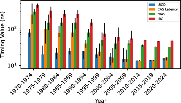
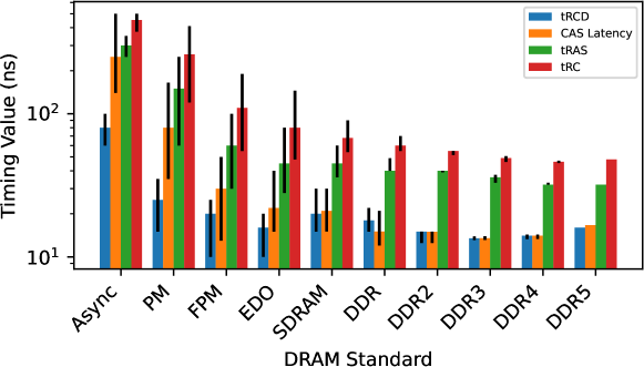
Figure 8.5 shows the minimum, median, and maximum of the timing parameter values (in log scale) grouped by DRAM chip storage capacity.151515We omit tRCD and tRAS for the 1 Kib chips because they do not use a row address strobe (RAS) signal. We find that the timings follow similar trends as in Figure 8.4 because higher-capacity DRAM chips are typically introduced more recently and follow newer DRAM standards.
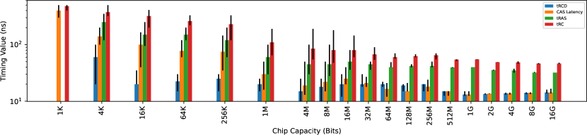
8.A.2 Current Consumption Trends
We review the evolution of the following key DRAM current consumption measurements, which are standardized by JEDEC and are provided by manufacturers in their datasheets.
-
•
IDD0: current consumption with continuous row activation and precharge commands issued to only one bank.
-
•
IDD4R: current consumption when issuing back-to-back read operations to all banks.
-
•
IDD5B: current consumption when issuing continuous burst refresh operations.
Figure 8.6 shows how key DRAM current consumption values (in log scale) have evolved across DRAM chips of different years (top) and capacities (bottom). We use different markers to show data points from chips of different DRAM standards. We qualitatively observe that current consumption increased exponentially up until approximately the year 2000, which is about the time at which improvements in access timings slowed down (as seen in Figure 2.3.4). After this point, different current consumption measurements diverged as IDD0 values decreased while IDD4R and IDD5B stabilized or increased. We explain this behavior by a change in the way DRAM chips were refreshed as DRAM capacities continued to increase. Earlier DRAM chips refreshed rows using individual row accesses (e.g., RAS-only refresh), which result in comparable behavior for access and refresh operations. In contrast, newer DRAM chips aggressively refresh multiple rows per refresh operation (e.g., burst refresh), which differentiates refresh operations from normal row accesses [418, 49, 48].
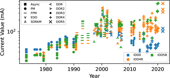
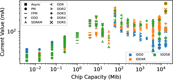
We quantify the current consumption values by aggregating the data points from Figure 8.6 by time and DRAM standard. Figure 8.7 shows the minimum, median, and maximum values (in log scale) across each 5-year period (top) and DRAM standard (bottom). The data shows that the median IDD0/IDD4R/IDD5B increased by 12.22/20.91/26.97% per year on average between 1970 and 2000 but decreased by 4.62/1.00/0.13% between 2000 and 2015161616Similar to Section LABEL:position:subsec:timing_trends, we omit the 2020 data point because the first-generation DDR5 chips exhibit outlying data values (e.g., no data reported for IDD5B in the datasheets). for an overall increase of 0.96/11.5/17.5% between 1970 and 2015.
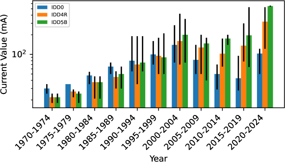
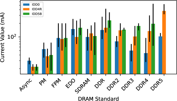
8.A.3 Relationship Between Timings and Currents
Finally, we examine the high-level relationship between the timing parameter and current consumption values. We find that the two are generally inversely related, which follows from the general principle that faster DRAM chips (i.e., lower timing parameters) require more power (i.e., increased current consumption values). Figure 8.8 illustrates this relationship for the four timing parameters studied in Section LABEL:position:subsec:timing_trends relative to IDD4R (i.e., the current consumption of read operations).
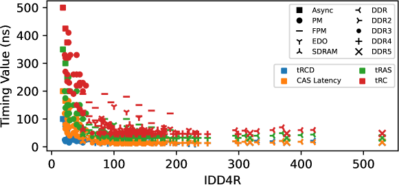
8.A.4 DRAM Refresh Timing Trends
DRAM refresh is governed by two key timing parameters:
-
•
tREFI (refresh interval): time between consecutive refresh commands sent by the memory controller.
-
•
tRFC: duration of a single refresh command.
Figure 8.9 shows how tREFI (left y-axis) and tRFC (right y-axis) evolved across the DRAM chips in our study. We group chips by storage capacity because DRAM refresh timings are closely related to capacity: higher-capacity chips using the same technology require more time or more refresh operations to fully refresh. The error bars show the minimum and maximum values observed across all chips for any given chip capacity.
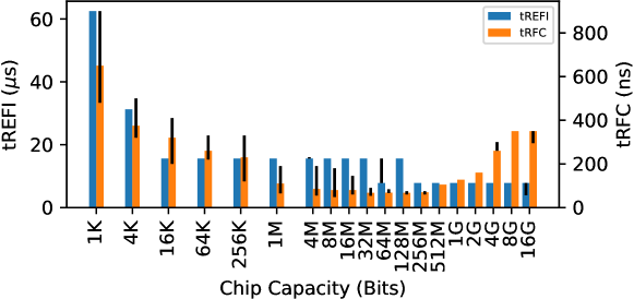
We make three observations. First, tREFI is shorter for higher-capacity DRAM chips (e.g., 62.5 s for an asynchronous 1 Kib chip versus 3.9 s for a 16 Gib DDR5 chip). This is consistent with the fact that higher-capacity chips require more frequent refreshing. Second, tRFC first decreases with chip capacity (e.g., 900 ns for an asynchronous 1 Kib chip versus 54 ns for a 32 Mib SDRAM chip) but then increases (e.g., to 350 ns for a 16 Gib DDR4 chip). This is because rapid improvements in row access times (and therefore refresh timings) initially outpaced the increase in storage capacity. However, starting around 512 Mib chip sizes, row access times improved much more slowly (as observed in Section LABEL:position:subsec:timing_trends) while storage capacity continued to increase. Third, the variation in tRFC across chips of each capacity (illustrated using the error bars) decreased for higher-capacity chips. This is because higher-capacity chips follow more recent DRAM standards (i.e., DDRn), which standardize DRAM auto refresh timings. In contrast, older DRAM chips were simply refreshed as quickly as their rows could be accessed (e.g., every tRC using RAS-only refresh).
Figure 8.10 shows the refresh penalty [48, 49], which is defined as the ratio between tRFC and tREFI, for DRAM chips of different storage capacities. The refresh penalty represents the average time that a DRAM rank (or bank) is unavailable for access due to refresh operations [48, 544, 49, 104, 624]. We observe that the refresh penalty exhibits a similar trend to tRFC: the refresh penalty worsens from a median of 1.04% for 1 Kib chips to 2.05% for 16 Kib chips, then improves to 0.43% for 128 Mib chips, and finally worsens to a median of 4.48% (worst-case of 7.56% for DDR5 chips) for 16 Gib chips.
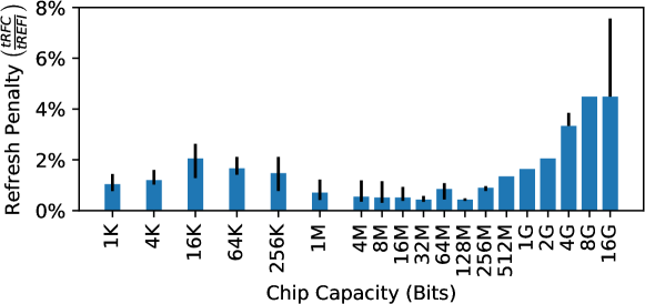
This non-monotonic trend is due to the relative improvements in DRAM access times and storage capacities: DRAM capacities consistently improved while DRAM access times did so only for older, lower-capacity chips (e.g., Mib chips). This is consistent with trends observed in prior work [443, 370, 59, 431, 92, 480], which expect that future, higher-capacity DRAM chips will spend an even larger proportion of time refreshing unless the DRAM refresh algorithm and techniques can be improved.
?appendixname? 8.B Survey Data Sources
Table 8.2 itemizes the 58 DRAM datasheets used for our survey in Appendix LABEL:position:appendix_a. For each datasheet, we show the DRAM chip manufacturer, model number, DRAM standard, year, and capacity. Our full dataset is available online [2].
| Year | Manufacturer | Model Number | Datasheet Source | DRAM Standard | Capacity per Chip (Kib) |
|---|---|---|---|---|---|
| 1970 | Intel | 1103 | \citeSds_intel19701103 | Asynchronous | 1 |
| 1971 | Mostek | MK4006 | \citeSds_mostek1971mk4006 | Asynchronous | 1 |
| 1973 | Mostek | MK4096 | \citeSds_mostek1973mk4096 | Asynchronous | 4 |
| 1976 | Mostek | MK4027 | \citeSds_mostek1976mk4027 | PM | 4 |
| 1976 | Mostek | MK4116P | \citeSds_mostek1976mk4116p | PM | 16 |
| 1978 | Fairchild | F4116 | \citeSds_fairchild1978f4116 | PM | 16 |
| 1979 | Intel | 2118 | \citeSds_intel19792118 | PM | 16 |
| 1981 | Mitsubishi | M5K4164ANP | \citeSds_mitsubishi1981m5k4164anp | PM | 64 |
| 1982 | Mostek | MK4564 | \citeSds_mostek1982mk4564 | PM | 64 |
| 1984 | NTE | NTE4164 | \citeSds_nte1984nte4164 | PM | 64 |
| 1984 | Texas Instruments | TMS4416 | \citeSds_texas1984tms4416 | PM | 64 |
| 1985 | Mitsubishi | M5M4256P | \citeSds_mitsubishi1985m5m4256p | PM | 256 |
| 1987 | Samsung | KM41464A | \citeSds_samsung1987km41464a | PM | 256 |
| 1987 | Texas Instruments | TMS4464 | \citeSds_texas1987tms4464 | PM | 256 |
| 1989 | Texas Instruments | SMJ4464 | \citeSds_texas1989smj4464 | PM | 256 |
| 1990 | Intel | 21256 | \citeSds_intel199021256 | PM | 256 |
| 1991 | Mitsubishi | M5M44100 | \citeSds_mitsubishi1991m5m44100 | FPM | 4096 |
| 1993 | Mitsubishi | M5M44256B | \citeSds_mitsubishi1993m5m44256b | FPM | 1024 |
| 1993 | Mosel Vitelic | V404J8 | \citeSds_mosel1993v404j8 | FPM | 8192 |
| 1995 | Siemens | HYB511000BJ | \citeSds_siemens1995hyb511000bj | FPM | 1024 |
| 1997 | Hyundai | HY5118164B | \citeSds_hyundai1997hy5118164b | EDO | 16384 |
| 1997 | Samsung | KM48S2020CT | \citeSds_samsung1997km48s2020ct | SDRAM | 16384 |
| 1998 | Micron | MT48LC4M4A1 | \citeSds_micron1998mt48lc4m4a1 | SDRAM | 16384 |
| 1998 | Mosel Vitelic | V53C808H | \citeSds_mosel1998v53c808h | EDO | 8192 |
| 1998 | Siemens | HYB39S16400 | \citeSds_siemens1998hyb39s16400 | SDRAM | 16384 |
| 1999 | Samsung | K4S160822D | \citeSds_samsung1999k4s160822d | SDRAM | 16384 |
| 1999 | Samsung | K4S561632A | \citeSds_samsung1999k4s561632a | SDRAM | 262144 |
| 2000 | Amic | A416316B | \citeSds_amic2000a416316b | FPM | 1024 |
| 2000 | ISSI | IS41LV32256 | \citeSds_issi2000is41lv32256 | EDO | 8192 |
| 2000 | Samsung | K4D623237A5 | \citeSds_samsung2000k4d623237a5 | DDR | 65536 |
| 2001 | Alliance | AS4C256K16E0 | \citeSds_alliance2001as4c256k16e0 | EDO | 4096 |
| 2001 | Alliance | AS4C4M4FOQ | \citeSds_alliance2001as4c4m4foq | FPM | 16384 |
| 2001 | ISSI | IS41C4400X | \citeSds_issi2001is41c4400x | EDO | 16384 |
| 2001 | Micron | MT46V2M32 | \citeSds_micron2001mt46v2m32 | DDR | 65536 |
| 2001 | Micron | MT46V32M4 | \citeSds_micron2001mt46v32m4 | DDR | 131072 |
| 2001 | Mosel Vitelic | V58C265164S | \citeSds_mosel2001v58c265164s | DDR | 65536 |
| 2001 | TM Tech | T224160B | \citeSds_tm2001t224160b | FPM | 4096 |
| 2003 | Micron | MT46V64M4 | \citeSds_micron2003mt46v64m4 | DDR | 262144 |
| 2003 | Samsung | K4S560432E | \citeSds_samsung2003k4s560432e | SDRAM | 262144 |
| 2005 | Amic | A43L0632 | \citeSds_amic2005a43l0632 | SDRAM | 32768 |
| 2006 | Elite | M52S32321A | \citeSds_elite2006m52s32321a | SDRAM | 32768 |
| 2006 | ISSI | IS42S81600B | \citeSds_issi2006is42s81600b | SDRAM | 131072 |
| 2006 | Sasmung | K4T51043QC | \citeSds_sasmung2006k4t51043qc | DDR2 | 524288 |
| 2007 | Micron | MT47H256M4 | \citeSds_micron2007mt47h256m4 | DDR2 | 1048576 |
| 2010 | Samsung | K4B4G0446A | \citeSds_samsung2010k4b4g0446a | DDR3 | 4194304 |
| 2011 | Hynix | H5TQ4G43MFR | \citeSds_hynix2011h5tq4g43mfr | DDR3 | 4194304 |
| 2011 | Nanya | NT5CB512M | \citeSds_nanya2011nt5cb512m | DDR3 | 2097152 |
| 2013 | Samsung | K4B4G0446A | \citeSds_samsung2013k4b4g0446a | DDR3 | 4194304 |
| 2015 | Micron | MT40A2G | \citeSds_micron2015mt40a2g | DDR4 | 8388608 |
| 2016 | Hynix | H5AN4G4NAFR | \citeSds_hynix2016h5an4g4nafr | DDR4 | 4194304 |
| 2016 | Samsung | K4A8G165WC | \citeSds_samsung2016k4a8g165wc | DDR4 | 8388608 |
| 2017 | Hynix | H5AN8G4NAFR | \citeSds_hynix2017h5an8g4nafr | DDR4 | 8388608 |
| 2018 | Micron | MT40A | \citeSds_micron2018mt40a | DDR4 | 16777216 |
| 2019 | Hynix | H5AN8G4NCJR | \citeSds_hynix2019h5an8g4ncjr | DDR4 | 8388608 |
| 2019 | Samsung | K4AAG045WA | \citeSds_samsung2019k4aag045wa | DDR4 | 16777216 |
| 2020 | Samsung | K4AAG085WA | \citeSds_samsung2020k4aag085wa | DDR4 | 16777216 |
| 2021 | Hynix | HMCG66MEB | \citeSds_hynix2021hmcg66meb | DDR5 | 16777216 |
| 2021 | Micron | MT60B1G16 | \citeSds_micron2021mt60b1g16 | DDR5 | 16777216 |
IEEEtran \bibliographySreferences
?chaptername? 9 Conclusions and Future Directions
In summary, the goal of this dissertation is twofold: (1) understand how on-die ECC obfuscates the raw memory error characteristics; and (2) develop new testing techniques that enable scientists and engineers to overcome the obfuscation. To this end, we use a combination of analytical and experimental studies to develop a series of new testing techniques that allow for faster, more effective error profiling and recovery of the error characteristics that on-die ECC obfuscates.
First, we perform the first extensive error characterization study of data-retention errors in LPDDR4 DRAM chips in order to understand how the errors occur and develop a fast and efficient error profiling algorithm. We find that there is a complex tradeoff space surrounding data-retention error profiling, where profiling under different operating conditions can improve profiling runtime and coverage at the cost of incurring false positives. Based on this, we introduce reach profiling, a new data-retention error profiling algorithm that searches for errors at a longer refresh interval and/or higher temperature than the desired operating conditions in order to improve profiling runtime and coverage. Our evaluations show that reach profiling can improve runtime by an average of 2.5 relative to the best prior profiling algorithm while achieving 99% coverage with less than a 50% false positive rate.
Second, we extend our studies to DRAM chips that use on-die ECC. To understand how on-die ECC affects DRAM data-retention error characteristics, we develop Error Inference (EIN), a new statistical inference methodology capable of inferring details of both the on-die ECC mechanism and the underlying raw bit errors using only the processor-visible post-correction errors. We evaluate EIN through the first data-retention error characterization study of DRAM chips that use on-die ECC. We find that EIN is able to (1) reverse-engineer the type and strength of the on-die ECC implementation; (2) infer pre-correction data-retention error rates given only the post-correction errors; and (3) recover the well-studied raw bit error distributions that on-die ECC obfuscates.
Third, to understand exactly how on-die ECC acts upon a given raw bit error pattern, we develop a new testing methodology, Bit-Exact Error Recovery (BEER). BEER systematically determines the full on-die ECC function (i.e., its parity-check matrix) without requiring access to hardware tools, prerequisite knowledge about the DRAM chip or the on-die ECC mechanism, or ECC metadata (e.g., error syndromes, parity information). We demonstrate BEER using 80 real LPDDR4 DRAM and evaluate its correctness and performance in simulation. We then introduce Bit-Exact Error Profiling (BEEP), the first error profiling algorithm that uses the known on-die ECC function (e.g., via BEER) to recover the number and bit-exact locations of the pre-correction errors that are responsible for a given post-correction error pattern.
Fourth, we study how on-die ECC operations alter the memory controller’s perspective of memory errors in order to understand how on-die ECC impacts error profiling. Based on our study, we identify three key challenges that on-die ECC introduces, each stemming from the fact that on-die ECC introduces statistical dependence between otherwise independent errors. To overcome these challenges, we introduce Hybrid Active-Reactive Profiling (HARP), a new bit-granularity error profiling algorithm. HARP uses small modifications to the on-die ECC read logic to enable fast and efficient error profiling in the presence of on-die ECC. Our evaluations show that HARP significantly improves profiling speed relative to baseline profiling algorithms that rely only on post-correction errors.
Finally, based on the understanding and insights we developed through the course of our work, we argue the importance of having transparency into basic DRAM reliability characteristics so that system designers can more easily implement a broad range of optimizations for better adapting commodity DRAM chips to the particular needs of their systems. We substantiate our arguments through three case studies: (1) reducing DRAM refresh overhead; (2) improving DRAM access latency; and (3) designing RowHammer defenses. In each study, we highlight the lack of transparency that discourages system designers from adopting the optimization. We conclude by providing our recommendations for improving transparency in current and future commodity DRAM-based systems.
9.1 Future Research Directions
Although this dissertation focuses on testing techniques to overcome on-die ECC primarily in the context of DRAM errors, we believe that this work is applicable in a more general sense and opens up new research directions. This section reviews promising directions for future work.
9.1.1 Extending the Proposed Techniques
We believe that the general principles behind each of our techniques are applicable to other ECC designs (e.g., stronger linear block codes such as Bose-Chaudhuri-Hocquenghem (BCH) [69, 210] and Reed-Solomon (RS) [489] codes) and architectures (e.g., rank-level ECC), failure modes (e.g., RowHammer), and memory technologies and (e.g., NAND Flash memory [78], phase-change memory [598, 339, 340], magnetoresistive memory [29, 632], Racetrack memory [463]). In this section, we review several directions in which we believe our work can be adapted to identify and address reliability challenges in other systems.
To Other ECC Schemes
Although we demonstrate EIN, BEER, and HARP in the context of DRAM on-die ECC, the techniques we rely upon are not restricted to single-error correcting Hamming code. EIN is broadly applicable because it only requires understanding how a given ECC mechanism will transform the statistical characteristics of the pre-correction errors. As long as this transformation can be understood for a given ECC scheme (e.g., using simulations, as we do in our work), EIN can be extended to deduce the nature of the ECC scheme and the pre-correction errors it obfuscates. Similarly, BEER and HARP rely upon how the syndrome decoding process treats uncorrectable errors. This process is not specific to Hamming codes, and in fact, can be used by all linear block codes, including BCH and RS codes that are useful for stronger, multi-bit error correction outside of the memory die. Therefore, we believe future work can take inspiration from and extend our work to develop analogous techniques for systems using different, possibly stronger ECC schemes.
To Other DRAM Failure Modes
We demonstrate our work in the context of DRAM data-retention errors because they are a relevant and interesting problem today. However, we believe that future work can apply similar principles to those underlying our techniques (e.g., profiling under exacerbated operating conditions, exploiting data-dependence of the error mechanisms) to solve error profiling and characterization challenges for other DRAM failure modes. For example, several works [611, 505, 459] analytically and/or experimentally demonstrate that RowHammer exhibits sensitivity to device temperature. Based on this observation, reach profiling can potentially be extended to quickly and efficiently identify those cells that are more susceptible to RowHammer errors. In general, any failure mode that is sensitive one or more parameters that are under the operator’s control (e.g., data patterns, timings, temperature, voltage) can theoretically be exploited in such a manner.
Similarly, a BEER-like approach can be taken with any failure mode that exhibits strong dependence on the data value stored in a cell. This data dependence allows control over which cells can and cannot fail, enabling the extraction of information about the ECC mechanism and raw bit error characteristics. Although other DRAM failure modes have not been shown to exhibit as strong a data dependence as data-retention, we believe that BEER can be extended to work with a failure mode that exhibits some amount of data dependence through creative use of statistical measurements.
To Unpredictable Failure Modes
Our studies and techniques are centered on observing large quantities of uncorrectable errors in order to infer information about the on-die ECC mechanism and raw bit errors. However, addressing difficult-to-predict errors (e.g., sporadic events such as VRT errors) is already a significant challenge in DRAM today [405] and will continue to worsen with technology scaling. Unfortunately, these errors are difficult to anticipate beforehand (e.g., with offline profiling), so understanding their characteristics and developing efficient techniques to combat them is an important problem.
To Emerging Memory Technologies
Our work provides researchers with the tools to understand and explore DRAM on-die ECC and the raw bit error characteristics. However, the analysis and techniques we contribute are not limited to DRAM and can theoretically be extended to work with other memory technologies, such as PCM, MRAM, and RM. These technologies are known to suffer from their own reliability challenges [339, 340, 358, 306, 239, 275, 33, 570, 97, 29, 430, 110, 487], potentially requiring approaches similar to on-die ECC to make manufacturing feasible.111In fact, certain commodity STT-MRAM chips [144] are already provisioned with on-die ECC. Although most of these technologies are yet to be productized, identifying feasible designs and architectures is an important research problem that will continue to become more relevant as the technologies mature. We believe that our work will be relevant and helpful in addressing challenges that arise from on-die error-mitigation techniques that these memories incorporate.
To Other ECC Architectures
At an abstract level, our work applies to any communication channel that suffers from statistically well-defined errors and only exposes post-correction data. DRAM on-die ECC is an ideal example because all error-mitigation operations occur within the DRAM die and are therefore invisible at the chip’s interface. Furthermore, DRAM failure modes are closely tied to the technology itself and have been studied extensively across decades of research. However, any memory architecture that provides no visibility into the ECC mechanism likely suffers from analogous challenges to those we identify in our work. Possible examples include (1) a memory architecture that places ECC within an in-package memory controller (e.g., as does NAND Flash), thereby making the ECC invisible to the rest of the system; and (2) a DRAM-based system that uses rank-level ECC (i.e., within the memory controller). Although the ECC’s internal workings are more accessible than on-die ECC in both of these examples [115], a scientist or engineer who does not have access to the interfaces that allow visibility into the ECC mechanism (e.g., special processor registers, hardware debugging interfaces) can extend the techniques that we provide in our work to conduct their studies.
9.1.2 Leveraging the New-Found Visibility into Error Characteristics
We believe that future work can use the techniques that we develop in this work to enable a broad range of more robust systems in the context of memory chips that use on-die ECC. We review several possibilities in this section, but believe that other use cases exist that we have not yet foreseen.
Improved System-Level Error Mitigations
Armed with the tools to better understand on-die ECC, system designers can adapt their own error-mitigation mechanisms to the on-die ECC mechanisms that memory manufacturers deploy. This is especially important for systems that integrate modern commodity DRAM because on-die ECC is already prevalent among LPDDR4 and DDR5 chips [447, 333, 330, 253]. Several works [538, 88, 177] argue the value of being aware of on-die ECC when designing system-level error-mitigation mechanisms, and techniques such as EIN and BEER enable this visibility for already-deployed memory chips that use on-die ECC.
Error-Tolerant Computing
Prior works [562, 326, 442] have used their understanding of DRAM error characteristics to make neural network applications tolerant to DRAM errors. For such applications, we believe this is a promising approach to circumvent the need for stronger, more expensive hardware error-mitigation mechanisms. As with designing robust systems, making an application resilient to errors requires understanding the errors’ characteristics. We believe that the techniques we contribute will allow researchers to extend existing techniques and develop new ones that target systems equipped with on-die ECC.
9.1.3 Alternative Error Mitigation Designs
Our work details key challenges that on-die ECC’s obfuscation of error characteristics entails. We believe that modifying or replacing on-die ECC with techniques that avoid obfuscating the underlying error characteristics is a crucial future research direction. Although these approaches cannot help for DRAM on-die ECC that pervades DRAM chips today, we believe that they are promising alternatives for future designs.
Alternative On-Die ECC Architectures
Recent work [435, 177, 258] has considered rearchitecting on-die ECC in ways that allow system designers to better complement the reliability benefits that on-die ECC already provides. Similarly, recent DDR5 DRAM standards [253] explicitly discuss on-die ECC within specifications and add limited functionality to expose the underlying reliability characteristics (e.g., a limited form of ECC scrubbing). Each of these approaches take important steps towards enabling DRAM consumers to extract the maximum benefit from on-die ECC while minimizing the downsides (e.g., that we identify and work to address in this dissertation). However, we believe that significant future work remains to identify the best possible on-die ECC designs for different system configurations, design goals, and target error rates.
System-Level Error Mitigations
As memory errors worsen with continued technology scaling, we expect memory manufacturers to consider even stronger on-die ECC mechanisms. As an alternative to on-die ECC, we believe it is important to explore other ways to mitigate high error rates. Different system components have different advantages with respect to error mitigation. For example, the software is well-equipped to determine which errors are and are not significant at the application-level [396, 361, 381] and address them using flexible software-level techniques (e.g., using redundancy [528, 557, 490, 527] and/or failure recovery mechanisms [146, 96, 477]). In contrast, the hardware can quickly and efficiently respond to errors that occur during runtime [388]. We believe that exploring the system-level design space for error mitigation is a promising direction, not only to tackle high error rates that are difficult to address using on-die ECC or hardware repair mechanisms, but also to address the difficulties that proprietary on-die ECC solutions cause for system design and test.
9.1.4 Improving Transparency into DRAM Reliability and Operation
Our work explains and addresses the consequences of using on-die ECC that is completely invisible to the rest of the system. To prevent this problem in the future, we believe that an in-depth reevaluation of DRAM specifications is warranted. Although we identify certain information that can help DRAM consumers if released (discussed in Section 8.9), a broader study of areas in which design transparency can be helpful, possibly performed by system designers themselves, would be immensely helpful to guide future work.
9.2 Concluding Remarks
In this dissertation, we explore memory error characterization and profiling both with and without on-die ECC. We builds a detailed understanding of the challenges that on-die ECC introduces for when studying memory error characteristics. We show that on-die ECC obfuscates errors, making it difficult for scientists and engineers to make sense of observed errors in the context of the underlying physical memory technology. To address these challenges, we propose four new sets of testing techniques that enable more effectively study memory error characteristics: (1) Reach profiling, which quickly identifies bits at risk of data-retention error with high coverage so that refresh overhead mitigation techniques may safely eliminate unnecessary refresh operations; (2) EIN, which allows inferring details of both the on-die ECC mechanism and the raw bit error characteristics in the context of an error-characterization study; (3) BEER and BEEP, which expose the precise details of how on-die ECC is affecting raw bit error patterns, allowing for well informed design and test practices; and (4) HARP, which enables quickly identifying bits at risk of error in memory devices that use on-die ECC, thereby enabling bit repair mechanisms to accurately mitigate errors. We hope that the data and methods we contribute enable new studies and research directions that embrace the benefits of techniques like on-die ECC without sacrificing the transparency that we believe is crucial for continued innovation.
?appendixname? A Other Works of the Author
I led four successful projects that led towards this dissertation during my time as a Ph.D. student. First, I developed REAPER [468] with significant and foundational help from Jeremie Kim. Chapter 4 describes this project in detail, which was my first foray into the DRAM space. Second, I delved further into DRAM reliability with EIN [467], releasing the open-source, experimentally-validated EINSim [4] tool as part of the project. To our knowledge, EIN is the first work to delve into the real-world implementation of DRAM on-die ECC and received the Best Paper Award at DSN 2019. Chapter 5 summarizes this project and our findings. Next, I continued exploring the adverse consequences of on-die ECC with BEER [466], culminating in an open-source tool [1] that enables the community to replicate our study and freely apply the BEER methodology to their own devices. BEER received the best paper award at MICRO 2020 in recognition of its contributions to the state-of-the-art. Chapter 6 describes BEER and our open-source tool. Most recently, I developed HARP [465], whose artifacts are peer-evaluated and publicly available as an open-source tool [469, 5]. Chapter 7 discusses our study and findings from this project. Finally, I used the combined learnings from these projects (and other collaborations, described below) to develop a set of recommendations for the DRAM community going forward. Chapter 8 summarizes these recommendations, which we believe will improve the state of the industry in both the short and long term.
Throughout my graduate studies, I also participated in research projects in several distinct areas with my fellow graduate students in SAFARI. I acknowledge these works in the remainder of this chapter.
I spent the first year of my Ph.D. working in close collaboration with Amirali Boroumand. We devolved an efficient coherence protocol for processing-in-memory systems, culminating in two works: LazyPIM [67] and CoNDA [66]. In these works, we show that a speculative, optimistic approach to coherence traffic can be a good alternative to fine- or coarse-grained accounting given workloads that access the same data from both the host processor and the processing-in-memory cores.
Next, I delved into the DRAM reliability space and became involved with several works that I co-authored with Jeremie Kim alongside our work with data-retention errors. We performed extensive experimental DRAM error characterization studies, in which we exploited DRAM access timing reductions to (1) develop reliable device fingerprints in the form of physically unclonable functions (DRAM latency PUF [295]); (2) reduce memory access latency for memory locations that are tolerant to reduced access timings (Solar DRAM [294]); (3) and generate true random numbers (D-RaNGe [296]). Later, I was involved with Yaohua Wang in two projects. First, we improved the DRAM access latency by exploiting opportunities for reducing memory access timings based on an application’s memory access pattern (CAL [586]). Second, we developed a fine-grained in-DRAM data movement mechanism (FIGARO [585]) that can be exploited to act as a cache that improves the average DRAM access latency, in addition to potentially helping defend against security attacks that make use of RowHammer and DRAM timing side channels.
Continuing on the path of DRAM access latency reduction, I worked with Hasan Hassan to develop CROW [196], a mechanism that enables quickly duplicating data between rows in-DRAM. Using the copy operation, we show that it is possible to use the copied rows to reduce both access latency and refresh overheads. Next, I worked with Haocong Luo to develop CLR-DRAM [376], a technique that enables a run time memory capacity-latency tradeoff at the granularity of individual DRAM rows. CLR-DRAM allows switching between the two states on the order of nanoseconds, providing a new and highly reconfigurable substrate for future research to build upon. Next, I worked with Lois Orosa to develop CODIC [454] a substrate that exposes fine-grained internal DRAM access timings to the programmer. Using these access timings, the programmer can implement a wide range of features, such as a physically unclonable function and a cold boot attack prevention mechanism. Finally, I worked with Ataberk Olgun to design QUAC-TRNG [452], a high-throughput true random number generator based on the error characteristics of commodity DRAM chips.
I also contributed on the topic of RowHammer through several distinct projects. First, I worked with Lucian Cojocar to study the effectiveness of different RowHammer error testing strategies and develop a methodology usable by server-class systems to test for RowHammer [113]. Next, I worked with Jeremie Kim to perform a large-scale RowHammer error-characterization study [297], in which we examined how RowHammer scales across different DRAM standards and technology generations. Then, I worked with Giray Yağlıkçı to develop BlockHammer [604], a new RowHammer defense mechanism that provides strong protection while improving scalability and compatibility with commodity DRAM chips relative to prior RowHammer defenses. Following BlockHammer, I worked with Lois Orosa and Giray Yağlıkçı to perform a large-scale RowHammer error-characterization study [455]. Finally, I worked with Giray Yağlıkçı to experimentally evaluate whether manipulating the DRAM supply voltage can be an effective defense against RowHammer [606].
Lastly, I worked with Nastaran Hajinazar on two different projects. In the first, we developed a new virtual memory framework called the Virtual Block Interface (VBI) [188]. VBI shifts the responsibility for most virtual memory management tasks to the hardware, thereby relieving the system software of significant complexity associated with virtual memory management responsibilities. In doing so, VBI improves overall system performance and enables several important architectural optimizations with respect to memory management. In the second project, we develop an end-to-end system framework for in-DRAM data processing called SIMDRAM [187]. SIMDRAM extends in-DRAM processing to a much more general set of computation primitives, facilitating the use of in-DRAM processing for a broader range of workloads.
?refname?
- [1] “BEER Source Code,” https://github.com/CMU-SAFARI/BEER.
- [2] “DRAM Datasheet Survey,” https://github.com/CMU-SAFARI/DRAM-Datasheet-Survey.
- [3] “DRAMPower Source Code,” https://github.com/ravenrd/DRAMPower.
- [4] “EINSim Source Code,” https://github.com/CMU-SAFARI/EINSim.
- [5] “HARP Source Code,” https://github.com/CMU-SAFARI/HARP.
- [6] “Ramulator Source Code,” https://github.com/CMU-SAFARI/ramulator.
- [7] “Standard Performance Evaluation Corporation,” http://www.spec.org/cpu2006.
- [8] Private communication, 2016–2021.
- [9] “DRAM: The Invention of On-Demand Data,” https://www.ibm.com/ibm/history/ibm100/us/en/icons/dram/transform/, 2021.
- [10] “Quarterly Report on Form 10-Q,” Micron Technologies, Inc., Tech. Rep., 2022.
- [11] 3D PLUS, “DDR4 SDRAM,” 2022.
- [12] R. D. Adams, High Performance Memory Testing: Design Principles, Fault Modeling and Self-Test. Springer SBM, 2002.
- [13] ADATA, “ADATA XPG DDR4 Officially Validated by AMD as AM4/Ryzen Compatible,” ADATA, Tech. Rep., 2017.
- [14] I. Advanced Validation Labs, “AVL Testing and Validation FAQ.”
- [15] Advantest, T5833/T5833ES Memory Test System, https://www.advantest.com/products/memory/t5833.html, 2022.
- [16] G. Agrawal, L. Massengill, and K. Gulati, “A Proposed SEU Tolerant Dynamic Random Access Memory (DRAM) Cell,” IEEE Trans. Nucl. Sci., 1994.
- [17] J. Ahn, S. Hong, S. Yoo, O. Mutlu, and K. Choi, “A Scalable Processing-In-Memory Accelerator for Parallel Graph Processing,” ISCA, 2016.
- [18] J. Ahn, S. Yoo, O. Mutlu, and K. Choi, “PIM-Enabled Instructions: A Low-Overhead, Locality-Aware Processing-in-Memory Architecture,” in ISCA, 2015.
- [19] B. Aichinger, “DDR Memory Errors Caused by Row Hammer,” in HPEC, 2015.
- [20] Z. Al-Ars, “DRAM Fault Analysis and Test Generation,” Ph.D. dissertation, Technische Universiteit Delft, 2005.
- [21] Z. Al-Ars, S. Hamdioui, and A. J. van de Goor, “Effects of Bit Line Coupling on the Faulty Behavior of DRAMs,” in VTS, 2004.
- [22] I. Alam, “Lightweight Opportunistic Memory Resilience,” Ph.D. dissertation, University of California, Los Angeles, 2021.
- [23] A. R. Alameldeen, I. Wagner, Z. Chishti, W. Wu, C. Wilkerson, and S.-L. Lu, “Energy-Efficient Cache Design Using Variable-Strength Error-Correcting Codes,” ISCA, 2011.
- [24] Alliance Memory, “Reliability Qualification Report,” Alliance Memory, Tech. Rep., 2014.
- [25] 2Gb/4Gb/8Gb LPDDR4, Alliance Memory, 2020, rev. 1.0.
- [26] AMD, “BKDG for AMD NPT Family 0Fh Processors,” 2009.
- [27] AMD, “BKDG for AMD Family 15h Models 00h-0Fh Processors,” 2013.
- [28] AMD, “AMD Opteron 4300 Series Processors,” 2018.
- [29] D. Apalkov, A. Khvalkovskiy, S. Watts, V. Nikitin, X. Tang, D. Lottis, K. Moon, X. Luo, E. Chen, A. Ong, A. Driskill-Smith, and M. Krounbi, “Spin-Transfer Torque Magnetic Random Access Memory (STT-MRAM),” JETC, 2013.
- [30] Apple Inc., “About the Security Content of Mac EFI Security Update 2015-001,” https://support.apple.com/en-us/HT204934, 2015.
- [31] ATP Electronics, “Stringent Tests from ICs to Modules Ensure DRAM Reliability,” https://www.atpinc.com/blog/dram-testing-module-chips-ic-burn-in-quality-characteristics, 2018.
- [32] J.-L. Autran, P. Roche, S. Sauze, G. Gasiot, D. Munteanu, P. Loaiza, M. Zampaolo, and J. Borel, “Altitude And Underground Real-Time SER Characterization Of CMOS 65 Nm SRAM,” IEEE Trans. Nucl. Sci., 2009.
- [33] M. Awasthi, M. Shevgoor, K. Sudan, B. Rajendran, R. Balasubramonian, and V. Srinivasan, “Efficient Scrub Mechanisms for Error-Prone Emerging Memories,” in HPCA, 2012.
- [34] Z. B. Aweke, S. F. Yitbarek, R. Qiao, R. Das, M. Hicks, Y. Oren, and T. Austin, “ANVIL: Software-Based Protection Against Next-Generation Rowhammer Attacks,” in ASPLOS, 2016.
- [35] A. Bacchini, M. Rovatti, G. Furano, and M. Ottavi, “Characterization of Data Retention Faults in DRAM Devices,” in DFT, 2014.
- [36] S. Baeg, D. Yun, M. Chun, and S.-J. Wen, “Estimation of the Trap Energy Characteristics of Row Hammer-Affected Cells in Gamma-Irradiated DDR4 DRAM,” IEEE Trans. Nucl. Sci., 2022.
- [37] S. Baek, S. Cho, and R. Melhem, “Refresh Now and Then,” in TC, 2014.
- [38] K. Bains, J. Halbert, C. Mozak, T. Schoenborn, and Z. Greenfield, “Row Hammer Refresh Command,” 2014, US Patent App. 13/539,415.
- [39] K. Bains, J. Halbert, C. Mozak, T. Schoenborn, and Z. Greenfield, “Row Hammer Refresh Command,” 2015, U.S. Patent 9,117,544.
- [40] K. S. Bains, R. Agarwal, and J. Lee, “Read Retry To Selectively Disable On-Die ECC,” 2020, US Patent App. 16/875,642.
- [41] K. S. Bains and J. B. Halbert, “Distributed Row Hammer Tracking,” 2016, U.S. Patent 9,299,400.
- [42] K. S. Bains and J. B. Halbert, “Row Hammer Monitoring Based on Stored Row Hammer Threshold Value,” 2016, U.S. Patent 9,384,821.
- [43] L. N. Bairavasundaram, A. C. Arpaci-Dusseau, R. H. Arpaci-Dusseau, G. R. Goodson, and B. Schroeder, “An Analysis Of Data Corruption In The Storage Stack,” TOS, 2008.
- [44] L. N. Bairavasundaram, G. R. Goodson, S. Pasupathy, and J. Schindler, “An Analysis Of Latent Sector Errors In Disk Drives,” in SIGMETRICS, 2007.
- [45] M. A. Bajura, Y. Boulghassoul, R. Naseer, S. DasGupta, A. F. Witulski, J. Sondeen, S. D. Stansberry, J. Draper, L. W. Massengill, and J. N. Damoulakis, “Models and Algorithmic Limits for an ECC-Based Approach To Hardening Sub-100-nm SRAMs,” Trans. on Nucl. Sci., 2007.
- [46] K. Baker and J. Van Beers, “Shmoo Plotting: The Black Art of IC Testing,” IEEE Des Test, 1997.
- [47] T. Baker, “Opening Up Ada-Tasking,” ACM SIGAda Ada Letters, 1990.
- [48] R. Balasubramonian, “A DRAM Refresh Tutorial,” http://utaharch.blogspot.com/2013/11/a-dram-refresh-tutorial.html, 2013.
- [49] R. Balasubramonian, “Innovations in the Memory System,” Synthesis Lectures on Computer Architecture, 2019.
- [50] S. K. Banerjee, “Two-Transistor DRAM Cell with High Alpha Particle Immunity,” 1989, US Patent 4,864,374.
- [51] A. Barenghi, L. Breveglieri, N. Izzo, and G. Pelosi, “Software-Only Reverse Engineering of Physical DRAM Mappings For RowHammer Attacks,” in IVSW, 2018.
- [52] E. Baseman, N. DeBardeleben, K. Ferreira, S. Levy, S. Raasch, V. Sridharan, T. Siddiqua, and Q. Guan, “Improving DRAM Fault Characterization Through Machine Learning,” in DSN-W, 2016.
- [53] J. Bauer, M. Gruhn, and F. C. Freiling, “Lest We Forget: Cold-Boot Attacks on Scrambled DDR3 Memory,” Digital Investigation, 2016.
- [54] L. Bautista-Gomez, F. Zyulkyarov, O. Unsal, and S. McIntosh-Smith, “Unprotected Computing: A Large-Scale Study Of DRAM Raw Error Rate On A Supercomputer,” in SC, 2016.
- [55] T. Bennett, S. Saroiu, A. Wolman, and L. Cojocar, “Panopticon: A Complete In-DRAM Rowhammer Mitigation,” in DRAMSec, 2021.
- [56] R. Bera, K. Kanellopoulos, A. Nori, T. Shahroodi, S. Subramoney, and O. Mutlu, “Pythia: A Customizable Hardware Prefetching Framework using Online Reinforcement Learning,” in MICRO, 2021.
- [57] R. Bera, A. V. Nori, O. Mutlu, and S. Subramoney, “DSPatch: Dual Spatial Pattern Prefetcher,” in MICRO, 2019.
- [58] I. Bhati, M.-T. Chang, Z. Chishti, S.-L. Lu, and B. Jacob, “DRAM Refresh Mechanisms, Penalties, and Trade-Offs,” in TC, 2016.
- [59] I. Bhati, Z. Chishti, S.-L. Lu, and B. Jacob, “Flexible Auto-Refresh: Enabling Scalable and Energy-Efficient DRAM Refresh Reductions,” in ISCA, 2015.
- [60] N. Bjørner, A.-D. Phan, and L. Fleckenstein, “nu-Z: An Optimizing SMT Solver,” in TACAS, 2015.
- [61] I. Boixaderas, D. Zivanovic, S. Moré, J. Bartolome, D. Vicente, M. Casas, P. M. Carpenter, P. Radojković, and E. Ayguadé, “Cost-Aware Prediction of Uncorrected DRAM Errors in the Field,” in SC, 2020.
- [62] S. Borkar and A. A. Chien, “The Future of Microprocessors,” CACM, 2011.
- [63] A. Boroumand, S. Ghose, B. Akin, R. Narayanaswami, G. F. Oliveira, X. Ma, E. Shiu, and O. Mutlu, “Google Neural Network Models for Edge Devices: Analyzing and Mitigating Machine Learning Inference Bottlenecks,” in PACT, 2021.
- [64] A. Boroumand, S. Ghose, B. Akin, R. Narayanaswami, G. F. Oliveira, X. Ma, E. Shiu, and O. Mutlu, “Mitigating Edge Machine Learning Inference Bottlenecks: An Empirical Study on Accelerating Google Edge Models,” arXiv:2103.00768, 2021.
- [65] A. Boroumand, S. Ghose, Y. Kim, R. Ausavarungnirun, E. Shiu, R. Thakur, D. Kim, A. Kuusela, A. Knies, P. Ranganathan, and O. Mutlu, “Google Workloads for Consumer Devices: Mitigating Data Movement Bottlenecks,” in ASPLOS, 2018.
- [66] A. Boroumand, S. Ghose, M. Patel, H. Hassan, B. Lucia, R. Ausavarungnirun, K. Hsieh, N. Hajinazar, K. T. Malladi, H. Zheng, and O. Mutlu, “CoNDA: Efficient Cache Coherence Support For Near-Data Accelerators,” in ISCA, 2019.
- [67] A. Boroumand, S. Ghose, M. Patel, H. Hassan, B. Lucia, K. Hsieh, K. T. Malladi, H. Zheng, and O. Mutlu, “LazyPIM: An Efficient Cache Coherence Mechanism For Processing-In-Memory,” CAL, 2016.
- [68] L. Borucki, G. Schindlbeck, and C. Slayman, “Comparison of Accelerated DRAM Soft Error Rates Measured at Component and System Level,” in IEEE IRPS, 2008.
- [69] R. C. Bose and D. K. Ray-Chaudhuri, “On a Class of Error Correcting Binary Group Codes,” Information and Control, 1960.
- [70] F. Bostancı, A. Olgun, L. Orosa, A. G. Yağlıkçı, J. S. Kim, H. Hassan, O. Ergin, and O. Mutlu, “DR-STRaNGe: End-to-End System Design for DRAM-based True Random Number Generators,” HPCA, 2022.
- [71] F. Brasser, L. Davi, D. Gens, C. Liebchen, and A.-R. Sadeghi, “CAn’t Touch This: Software-Only Mitigation Against Rowhammer Attacks Targeting Kernel Memory,” in USENIX Security, 2017.
- [72] R. Brummayer and A. Biere, “Boolector: An Efficient SMT Solver for Bit-Vectors and Arrays,” in International Conference on Tools and Algorithms for the Construction and Analysis of Systems, 2009.
- [73] G. W. Burr, M. J. Breitwisch, M. Franceschini, D. Garetto, K. Gopalakrishnan, B. Jackson, B. Kurdi, C. Lam, L. A. Lastras, A. Padilla, B. Rajendran, S. Raoux, and R. S. Shenoy, “Phase Change Memory Technology,” J Vac Sci Technol B, 2010.
- [74] Y. Cai, S. Ghose, E. F. Haratsch, Y. Luo, and O. Mutlu, “Error Characterization, Mitigation, and Recovery In Flash-Memory-Based Solid-State Drives,” Proc. IEEE, 2017.
- [75] Y. Cai, S. Ghose, E. F. Haratsch, Y. Luo, and O. Mutlu, “Errors in Flash-Memory-Based Solid-State Drives: Analysis, Mitigation, and Recovery,” Inside Solid State Drives, 2018.
- [76] Y. Cai, S. Ghose, Y. Luo, K. Mai, O. Mutlu, and E. F. Haratsch, “Vulnerabilities in MLC NAND Flash Memory Programming: Experimental Analysis, Exploits, and Mitigation Techniques,” in HPCA, 2017.
- [77] Y. Cai, E. F. Haratsch, M. McCartney, and K. Mai, “FPGA-Based Solid-State Drive Prototyping Platform,” in FCCM, 2011.
- [78] Y. Cai, E. F. Haratsch, O. Mutlu, and K. Mai, “Error Patterns in MLC NAND Flash Memory: Measurement, Characterization, and Analysis,” in DATE, 2012.
- [79] Y. Cai, E. F. Haratsch, O. Mutlu, and K. Mai, “Threshold Voltage Distribution in MLC NAND Flash Memory: Characterization, Analysis, and Modeling,” in DATE, 2013.
- [80] Y. Cai, Y. Luo, S. Ghose, and O. Mutlu, “Read Disturb Errors in MLC NAND Flash Memory: Characterization, Mitigation, and Recovery,” in DSN, 2015.
- [81] Y. Cai, Y. Luo, E. F. Haratsch, K. Mai, and O. Mutlu, “Data Retention in MLC NAND Flash Memory: Characterization, Optimization, and Recovery,” in HPCA, 2015.
- [82] Y. Cai, O. Mutlu, E. F. Haratsch, and K. Mai, “Program Interference in MLC NAND Flash Memory: Characterization, Modeling, and Mitigation,” in ICCD, 2013.
- [83] Y. Cai, G. Yalcin, O. Mutlu, E. F. Haratsch, A. Cristal, O. S. Unsal, and K. Mai, “Flash Correct-And-Refresh: Retention-Aware Error Management for Increased Flash Memory Lifetime,” in ICCD, 2012.
- [84] Y. Cai, G. Yalcin, O. Mutlu, E. F. Haratsch, A. Cristal, O. S. Unsal, and K. Mai, “Error Analysis and Retention-Aware Error Management for NAND Flash Memory,” in ITJ, 2013.
- [85] Y. Cai, G. Yalcin, O. Mutlu, E. F. Haratsch, O. Unsal, A. Cristal, and K. Mai, “Neighbor-Cell Assisted Error Correction for MLC NAND Flash Memories,” in SIGMETRICS, 2014.
- [86] G. C. Cardarilli, P. Marinucci, and A. Salsano, “Development of an Evaluation Model for the Design of Fault-Tolerant Solid State Mass Memory,” in ISCAS, 2000.
- [87] P. Cavicchi and R. Schellingerhout, “Patent Ambush in Standard-Setting: the Comission Accepts Commitments from Rambus to Lower Memory Chip Royalty Rates,” Competition Policy Newsletter, 2010.
- [88] S. Cha, O. Seongil, H. Shin, S. Hwang, K. Park, S. J. Jang, J. S. Choi, G. Y. Jin, Y. H. Son, H. Cho, J. H. Ahn, and N. S. Kim, “Defect Analysis and Cost-Effective Resilience Architecture for Future DRAM Devices,” in HPCA, 2017.
- [89] K. Chandrasekar, S. Goossens, C. Weis, M. Koedam, B. Akesson, N. Wehn, and K. Goossens, “Exploiting Expendable Process-Margins in DRAMs for Run-Time Performance Optimization,” in DATE, 2014.
- [90] K. K. Chang, “Understanding and Improving Latency of DRAM-Based Memory Systems,” Ph.D. dissertation, Carnegie Mellon University, 2017.
- [91] K. K. Chang, A. Kashyap, H. Hassan, S. Ghose, K. Hsieh, D. Lee, T. Li, G. Pekhimenko, S. Khan, and O. Mutlu, “Understanding Latency Variation in Modern DRAM Chips: Experimental Characterization, Analysis, and Optimization,” in SIGMETRICS, 2016.
- [92] K. K. Chang, D. Lee, Z. Chishti, A. R. Alameldeen, C. Wilkerson, Y. Kim, and O. Mutlu, “Improving DRAM Performance by Parallelizing Refreshes with Accesses,” in HPCA, 2014.
- [93] K. K. Chang, P. J. Nair, D. Lee, S. Ghose, M. K. Qureshi, and O. Mutlu, “Low-Cost Inter-Linked Subarrays (LISA): Enabling Fast Inter-Subarray Data Movement in DRAM,” in HPCA, 2016.
- [94] K. K. Chang, A. G. Yağlıkçı, S. Ghose, A. Agrawal, N. Chatterjee, A. Kashyap, D. Lee, M. O’Connor, H. Hassan, and O. Mutlu, “Understanding Reduced-Voltage Operation in Modern DRAM Devices: Experimental Characterization, Analysis, and Mechanisms,” in SIGMETRICS, 2017.
- [95] P. K. Chatterjee, G. W. Taylor, A. F. Tasch, and H.-S. Fu, “Leakage Studies in High-Density Dynamic MOS Memory Devices,” TED, 1979.
- [96] C. Chen, G. Eisenhauer, S. Pande, and Q. Guan, “Care: Compiler-Assisted Recovery From Soft Failures,” in SC, 2019.
- [97] E. Chen, D. Apalkov, Z. Diao, A. Driskill-Smith, D. Druist, D. Lottis, V. Nikitin, X. Tang, S. Watts, S. Wang, S. A. Wolf, A. W. Ghosh, J. W. Lu, S. J. Poon, M. Stan, W. H. Butler, S. Gupta, C. K. A. Mewes, T. Mewes, and P. B. Visscher, “Advances and Future Prospects of Spin-Transfer Torque Random Access Memory,” TOM, 2010.
- [98] H.-M. Chen, A. Arunkumar, C.-J. Wu, T. Mudge, and C. Chakrabarti, “E-ECC: Low Power Erasure And Error Correction Schemes For Increasing Reliability Of Commodity DRAM Systems,” in Proceedings of the 2015 International Symposium on Memory Systems, 2015, pp. 60–70.
- [99] H.-M. Chen, S.-Y. Lee, T. Mudge, C.-J. Wu, and C. Chakrabarti, “Configurable-ECC: Architecting a Flexible ECC Scheme to Support Different Sized Accesses in High Bandwidth Memory Systems,” TC, 2018.
- [100] H.-M. Chen, C.-J. Wu, T. Mudge, and C. Chakrabarti, “RATT-ECC: Rate Adaptive Two-Tiered Error Correction Codes for Reliable 3D Die-Stacked Memory,” ACM Transactions on Architecture and Code Optimization (TACO), vol. 13, no. 3, pp. 1–24, 2016.
- [101] J. Chen, X. Jiang, Y. Zhang, L. Liu, H. Xu, and Q. Liu, “CARE: Coordinated Augmentation for Elastic Resilience on DRAM Errors in Data Centers,” in HPCA, 2021.
- [102] L. Chen, Y. Cao, and Z. Zhang, “E3CC: A Memory Error Protection Scheme With Novel Address Mapping for Subranked And Low-Power Memories,” TACO, 2013.
- [103] K.-L. Cheng, M.-F. Tsai, and C.-W. Wu, “Neighborhood Pattern-Sensitive Fault Testing and Diagnostics for Random-Access Memories,” TCAD, 2002.
- [104] W.-K. Cheng, P.-Y. Shen, and X.-L. Li, “Retention-Aware DRAM Auto-Refresh Scheme for Energy and Performance Efficiency,” Micromachines, 2019.
- [105] B. R. Childers, J. Yang, and Y. Zhang, “Achieving Yield, Density and Performance Effective DRAM at Extreme Technology Sizes,” in MEMSYS, 2015.
- [106] M. H. Cho, N. Jeon, M. Jeong, S. Lee, S. Yamada, and H. Hong, “A Novel Method to Characterize DRAM Process Variation by the Analyzing Stochastic Properties of Retention Time Distribution,” in EDTM, 2017.
- [107] H. Choi, D. Hong, J. Lee, and S. Yoo, “Reducing DRAM Refresh Power Consumption by Runtime Profiling of Retention Time and Dual-Row Activation,” Microprocessors and Microsystems, 2020.
- [108] J. Choi, W. Shin, J. Jang, J. Suh, Y. Kwon, Y. Moon, and L.-S. Kim, “Multiple Clone Row DRAM: A Low Latency and Area Optimized DRAM,” in ISCA.
- [109] K. C. Chun, Y.-G. Chu, J.-S. Heo, T.-S. Kim, S. Kim, H.-K. Yang, M.-J. Kim, C.-K. Lee, J. Kim, H. Yoon et al., “A 16Gb LPDDR4X SDRAM with an NBTI-Tolerant Circuit Solution, an SWD PMOS GIDL Reduction Technique, an Adaptive Gear-Down Scheme and a Metastable-Free DQS Aligner In a 10nm Class DRAM Process,” in ISSCC, 2018.
- [110] K. C. Chun, H. Zhao, J. D. Harms, T.-H. Kim, J.-P. Wang, and C. H. Kim, “A Scaling Roadmap and Performance Evaluation of In-Plane and Perpendicular MTJ Based STT-MRAMs for High-Density Cache Memory,” JSSC, 2012.
- [111] A. Cimatti, A. Franzén, A. Griggio, R. Sebastiani, and C. Stenico, “Satisfiability Modulo The Theory of Costs: Foundations and Applications,” in TACAS, 2010.
- [112] G. C. Clark Jr and J. B. Cain, Error-Correction Coding for Digital Communications. Springer SBM, 2013.
- [113] L. Cojocar, J. Kim, M. Patel, L. Tsai, S. Saroiu, A. Wolman, and O. Mutlu, “Are We Susceptible to Rowhammer? An End-to-End Methodology for Cloud Providers,” in IEEE S&P, 2020.
- [114] L. Cojocar, K. Loughlin, S. Saroiu, B. Kasikci, and A. Wolman, “mFIT: A Bump-in-the-Wire Tool for Plug-and-Play Analysis of Rowhammer Susceptibility Factors,” 2021.
- [115] L. Cojocar, K. Razavi, C. Giuffrida, and H. Bos, “Exploiting Correcting Codes: On The Effectiveness Of ECC Memory Against Rowhammer Attacks,” in S&P, 2019.
- [116] D. J. Costello and S. Lin, Error Control Coding: Fundamentals and Applications. Prentice Hall, 1982.
- [117] F. Courbon, S. Skorobogatov, and C. Woods, “Reverse Engineering Flash EEPROM Memories Using Scanning Electron Microscopy,” in CARDIS, 2016.
- [118] T. M. Cover, J. A. Thomas, and J. Kieffer, “Elements of Information Theory,” SIAM Review, 1994.
- [119] K. Criss, K. Bains, R. Agarwal, T. Bennett, T. Grunzke, J. K. Kim, H. Chung, and M. Jang, “Improving Memory Reliability by Bounding DRAM Faults: DDR5 Improved Reliability Features,” in MEMSYS, 2020.
- [120] J. A. Croswell, “A Model for Analysis of the Effects of Redundancy and Error Correction on DRAM Memory Yield and Reliability,” Master’s thesis, MIT, 2000.
- [121] X. Cui, Z. Cheng, C. Lee, X. Lin, Y. Wei, X. Chen, and Z. Song, “A Snake Addressing Scheme for Phase Change Memory Testing,” SCIS, 2016.
- [122] Z. Cui, S. A. McKee, Z. Zha, Y. Bao, and M. Chen, “DTail: A Flexible Approach to DRAM Refresh Management,” in SC, 2014.
- [123] A. Das, H. Hassan, and O. Mutlu, “VRL-DRAM: Improving DRAM Performance Via Variable Refresh Latency,” in DAC, 2018.
- [124] Data Device Corporation, “Rad Hard Memories,” 2022.
- [125] H. David, C. Fallin, E. Gorbatov, U. R. Hanebutte, and O. Mutlu, “Memory Power Management via Dynamic Voltage/Frequency Scaling,” in ICAC, 2011.
- [126] L. De Moura and N. Bjørner, “Z3: An Efficient SMT Solver,” in TACAS, 2008.
- [127] F. de Ridder, P. Frigo, E. Vannacci, H. Bos, C. Giuffrida, and K. Razavi, “SMASH: Synchronized Many-sided Rowhammer Attacks from JavaScript,” in USENIX Security, 2021.
- [128] R. Dekker, F. Beenker, and L. Thijssen, “A Realistic Fault Model and Test Algorithms for Static Random Access Memories,” TCAD, 1990.
- [129] T. J. Dell, “A White Paper on the Benefits of Chipkill-Correct ECC for PC Server Main Memory,” IBM Microelectronics Division, 1997.
- [130] T. J. Dell, “System RAS Implications of DRAM Soft Errors,” IBM JRD, 2008.
- [131] Q. Deng, D. Meisner, L. Ramos, T. F. Wenisch, and R. Bianchini, “MemScale: Active Low-Power Modes for Main Memory,” in ASPLOS, 2011.
- [132] R. H. Dennard, “Field-Effect Transistor Memory,” 1968, US Patent 3,387,286.
- [133] R. H. Dennard, F. H. Gaensslen, H.-N. Yu, V. L. Rideout, E. Bassous, and A. R. LeBlanc, “Design of Ion-Implanted MOSFET’s with Very Small Physical Dimensions,” JSSC, 1974.
- [134] S. Desai, “Process Variation Aware DRAM (Dynamic Random Access Memory) Design Using Block-Based Adaptive Body Biasing Algorithm,” Ph.D. dissertation, Utah State University, 2012.
- [135] F. Devaux, “The True Processing in Memory Accelerator,” in HCS, 2019.
- [136] F. Devaux and R. Ayrignac, “Method and Circuit for Protecting a DRAM Memory Device from the Row Hammer Effect,” 2021, 10,885,966.
- [137] I. Dillig, T. Dillig, K. L. McMillan, and A. Aiken, “Minimum Satisfying Assignments for SMT,” in CAV, 2012.
- [138] A. Ditali, M. K. Ma, and M. Johnston, “X-Ray Radiation Effect in DRAM Retention Time,” T-DMR, 2007.
- [139] M. Duan, F. Adam-Lema, B. Cheng, C. Navarro, X. Wang, V. Georgiev, F. Gamiz, C. Millar, and A. Asenov, “2D-TCAD Simulation on Retention Time of Z2FET for DRAM Application,” in SISPAD, 2017.
- [140] K. Duganapalli, “Modelling and Test Generation for Crosstalk Faults in DSM Chips,” Ph.D. dissertation, Universität Bremen, 2016.
- [141] N. Edri, P. Meinerzhagen, A. Teman, A. Burg, and A. Fish, “Silicon-Proven, Per-Cell Retention Time Distribution Model for Gain-Cell Based eDRAMs,” IEEE TOCS, 2016.
- [142] B. Efron, “Bootstrap Methods: Another Look at the Jackknife,” in Breakthroughs in Statistics, 1992.
- [143] European Commission, “Competition Policy Newsletter,” Publications Office of the EU, 2010.
- [144] Everspin Technologies, “16Mb MRAM MR4A16B.”
- [145] S. Eyerman and L. Eeckhout, “System-Level Performance Metrics for Multiprogram Workloads,” in IEEE Micro, 2008.
- [146] B. Fang, Q. Guan, N. Debardeleben, K. Pattabiraman, and M. Ripeanu, “Letgo: A Lightweight Continuous Framework For HPC Applications Under Failures,” in HPDC, 2017.
- [147] M. Farmani, M. Tehranipoor, and F. Rahman, “RHAT: Efficient RowHammer-Aware Test for Modern DRAM Modules,” in ETS, 2021.
- [148] M. Ferdman, A. Adileh, O. Kocberber, S. Volos, M. Alisafaee, D. Jevdjic, C. Kaynak, A. D. Popescu, A. Ailamaki, and B. Falsafi, “Clearing The Clouds: A Study Of Emerging Scale-Out Workloads On Modern Hardware,” ASPLOS, 2012.
- [149] S. Field, “Microsoft Azure uses Error-Correcting Code Memory for Enhanced Reliability and Security,” https://azure.microsoft.com/en-us/blog/microsoft-azure-uses-error-correcting-code-memory-for-enhanced-reliability-and-security, 2015.
- [150] K. Flamm, “Measurement of DRAM Prices: Technology and Market Structure,” in Price Measurements and Their Uses. University of Chicago Press, 1993.
- [151] K. Flamm, “The Impact Of DRAM Design Innovation On Manufacturing Profitability,” Future Fab International, 2010.
- [152] G. D. Forney, “Concatenated Codes,” MIT Press, 1965.
- [153] P. Francis-Mezger and V. M. Weaver, “A Raspberry Pi Operating System for Exploring Advanced Memory System Concepts,” in MEMSYS, 2018.
- [154] P. Frigo, E. Vannacci, H. Hassan, V. van der Veen, O. Mutlu, C. Giuffrida, H. Bos, and K. Razavi, “TRRespass: Exploiting the Many Sides of Target Row Refresh,” in IEEE S&P, 2020.
- [155] R. Fromm, S. Perissakis, N. Cardwell, C. Kozyrakis, B. McGaughy, D. Patterson, T. Anderson, and K. Yelick, “The Energy Efficiency of IRAM Architectures,” ISCA, 1997.
- [156] FCRAM (Fast Cycle RAM), Fujitsu Semiconductor Limited, 2012, https://www.fujitsu.com/cn/Images/FCRAM_catalog_2012.2.pdf.
- [157] A. Fukami, S. Ghose, Y. Luo, Y. Cai, and O. Mutlu, “Improving the Reliability of Chip-Off Forensic Analysis of NAND Flash Memory Devices,” in Digital Investigation, 2017.
- [158] R. G. Gallager, “Low Density Parity Check Codes,” Ph.D. dissertation, Massachusetts Institute of Technology, 1963.
- [159] F. Gao, G. Tziantzioulis, and D. Wentzlaff, “ComputeDRAM: In-Memory Compute using Off-the-Shelf DRAMs,” in MICRO, 2019.
- [160] S. Gautam, S. Manhas, A. Kumar, M. Pakala, and E. Yieh, “Row Hammering Mitigation Using Metal Nanowire in Saddle Fin DRAM,” IEEE TED, 2019.
- [161] S. Ghose, A. Boroumand, J. S. Kim, J. Gómez-Luna, and O. Mutlu, “Processing-in-Memory: A Workload-driven Perspective,” IBM JRD, 2019.
- [162] S. Ghose, K. Hsieh, A. Boroumand, R. Ausavarungnirun, and O. Mutlu, “Enabling the Adoption of Processing-in-Memory: Challenges, Mechanisms, Future Research Directions,” arXiv:1802.00320, 2018.
- [163] S. Ghose, T. Li, N. Hajinazar, D. S. Cali, and O. Mutlu, “Demystifying Complex Workload-DRAM Interactions: An Experimental Study,” SIGMETRICS, 2019.
- [164] S. Ghose, A. G. Yağlıkçı, R. Gupta, D. Lee, K. Kudrolli, W. X. Liu, H. Hassan, K. K. Chang, N. Chatterjee, A. Agrawal, M. O’Connor, and O. Mutlu, “What Your DRAM Power Models Are Not Telling You: Lessons from a Detailed Experimental Study,” SIGMETRICS, 2018.
- [165] M. Ghosh and H.-H. S. Lee, “Smart Refresh: An Enhanced Memory Controller Design for Reducing Energy in Conventional and 3D Die-Stacked DRAMs,” in MICRO, 2007.
- [166] C. Giannoula, I. Fernandez, J. Gómez-Luna, N. Koziris, G. Goumas, and O. Mutlu, “Towards Efficient Sparse Matrix Vector Multiplication on Real Processing-in-Memory Architectures,” SIGMETRICS, 2022.
- [167] I. Giurgiu, J. Szabo, D. Wiesmann, and J. Bird, “Predicting DRAM Reliability in the Field with Machine Learning,” in Middleware, 2017.
- [168] V. Goiffon, T. Bilba, T. Deladerrière, G. Beaugendre, A. Le Roch, A. Dion, C. Virmontois, J.-M. Belloir, M. Gaillardin, A. Jay, and P. Paillet, “Radiation-Induced Variable Retention Time in Dynamic Random Access Memories,” IEEE Trans. Nucl. Sci., 2019.
- [169] M. Gokhale, B. Holmes, and K. Iobst, “Processing in Memory: The Terasys Massively Parallel PIM Array,” Computer, 1995.
- [170] S. M. Gold and A. B. Hegde, “Providing Test Coverage of Integrated ECC Logic in Embedded Memory,” 2014, US Patent 8,914,687.
- [171] C. P. Gomes, H. Kautz, A. Sabharwal, and B. Selman, “Satisfiability Solvers,” Foundations of Artificial Intelligence, 2008.
- [172] H. Gomez, A. Amaya, and E. Roa, “DRAM Row-Hammer Attack Reduction using Dummy Cells,” in NORCAS, 2016.
- [173] J. Gómez-Luna, I. El Hajj, I. Fernandez, C. Giannoula, G. F. Oliveira, and O. Mutlu, “Benchmarking Memory-Centric Computing Systems: Analysis of Real Processing-in-Memory Hardware,” in CUT, 2021.
- [174] J. Gómez-Luna, J. El Hajj, I. Fernandez, and C. Giannoula, “Benchmarking a New Paradigm: Understanding a Modern Processing-in-Memory Architecture,” in arXiv:2105.03814, 2021.
- [175] J. Gómez-Luna, I. E. Hajj, I. Fernández, C. Giannoula, G. F. Oliveira, and O. Mutlu, “Benchmarking a New Paradigm: Understanding a Modern Processing-in-Memory Architecture,” arXiv:2105.03814, 2021.
- [176] S.-L. Gong, J. Kim, and M. Erez, “DRAM Scaling Error Evaluation Model Using Various Retention Time,” in DSN-W, 2017.
- [177] S.-L. Gong, J. Kim, S. Lym, M. Sullivan, H. David, and M. Erez, “DUO: Exposing On-Chip Redundancy to Rank-Level ECC for High Reliability,” in HPCA, 2018.
- [178] S.-L. Gong, M. Rhu, J. Kim, J. Chung, and M. Erez, “Clean-ECC: High Reliability ECC for Adaptive Granularity Memory System,” in Proceedings of the 48th International Symposium on Microarchitecture, 2015, pp. 611–622.
- [179] K. W. Gorman, M. R. Ouellette, and P. E. Perry, “Memory Test With In-Line Error Correction Code Logic,” 2015, US Patent 9,224,503.
- [180] M. Gottscho, M. Shoaib, S. Govindan, B. Sharma, D. Wang, and P. Gupta, “Measuring The Impact Of Memory Errors On Application Performance,” CAL, 2016.
- [181] Z. Greenfield and T. Levy, “Throttling Support for Row-Hammer Counters,” 2016, U.S. Patent 9,251,885.
- [182] M. Gruhn and T. Müller, “On the Practicability of Cold Boot Attacks,” in ARES, 2013.
- [183] B. Gu, T. Coughlin, B. Maxwell, J. Griffith, J. Lee, J. Cordingley, S. Johnson, E. Karaginiannis, and J. Ehmann, “Challenges and Future Directions of Laser Fuse Processing in Memory Repair,” Proc. Semicon China, 2003.
- [184] X. Guo, M. N. Bojnordi, Q. Guo, and E. Ipek, “Sanitizer: Mitigating the Impact of Expensive ECC Checks on STT-MRAM Based Main Memories,” TOC, 2017.
- [185] S. Gurumurthi, K. Lee, M. Jang, V. Sridharan, A. Nygren, Y. Ryu, K. Sohn, T. Kim, and H. Chung, “HBM3: Enabling Memory Resilience at Scale,” CAL, 2021.
- [186] A. Gutierrez, R. G. Dreslinski, T. F. Wenisch, T. Mudge, A. Saidi, C. Emmons, and N. Paver, “Full-System Analysis And Characterization Of Interactive Smartphone Applications,” in IISWC, 2011.
- [187] N. Hajinazar, G. F. Oliveira, S. Gregorio, J. Ferreira, N. M. Ghiasi, M. Patel, M. Alser, S. Ghose, J. G. Luna, and O. Mutlu, “SIMDRAM: An End-to-End Framework for Bit-Serial SIMD Computing in DRAM,” ASPLOS, 2021.
- [188] N. Hajinazar, P. Patel, M. Patel, K. Kanellopoulos, S. Ghose, R. Ausavarungnirun, G. F. Oliveira, J. Appavoo, V. Seshadri, and O. Mutlu, “The Virtual Block Interface: A Flexible Alternative To The Conventional Virtual Memory Framework,” in ISCA, 2020.
- [189] J. A. Halderman, S. D. Schoen, N. Heninger, W. Clarkson, W. Paul, J. A. Calandrino, A. J. Feldman, J. Appelbaum, and E. W. Felten, “Lest We Remember: Cold-Boot Attacks on Encryption Keys,” USENIX Security, 2008.
- [190] T. Hamamoto, S. Sugiura, and S. Sawada, “Well Concentration: A Novel Scaling Limitation Factor Derived From DRAM Retention Time and Its Modeling,” in IEDM, 1995.
- [191] T. Hamamoto, S. Sugiura, and S. Sawada, “On the Retention Time Distribution of Dynamic Random Access Memory (DRAM),” in TED, 1998.
- [192] S. Hamdioui, P. Pouyan, H. Li, Y. Wang, A. Raychowdhur, and I. Yoon, “Test and Reliability of Emerging Non-Volatile Memories,” in ATS, 2017.
- [193] R. W. Hamming, “Error Detecting and Error Correcting Codes,” in Bell Labs Technical Journal, 1950.
- [194] Y. Han, Y. Wang, H. Li, and X. Li, “Data-Aware DRAM Refresh to Squeeze the Margin of Retention Time in Hybrid Memory Cube,” in ICCAD, 2014.
- [195] M. S. Hashemian, B. Singh, F. Wolff, D. Weyer, S. Clay, and C. Papachristou, “A Robust Authentication Methodology Using Physically Unclonable Functions in DRAM Arrays,” in DATE, 2015.
- [196] H. Hassan, M. Patel, J. S. Kim, A. G. Yağlıkçı, N. Vijaykumar, N. M. Ghiasi, S. Ghose, and O. Mutlu, “CROW: A Low-Cost Substrate for Improving DRAM Performance, Energy Efficiency, and Reliability,” in ISCA, 2019.
- [197] H. Hassan, G. Pekhimenko, N. Vijaykumar, V. Seshadri, D. Lee, O. Ergin, and O. Mutlu, “ChargeCache: Reducing DRAM Latency by Exploiting Row Access Locality,” in HPCA, 2016.
- [198] H. Hassan, Y. C. Tugrul, J. S. Kim, V. Van der Veen, K. Razavi, and O. Mutlu, “Uncovering In-DRAM RowHammer Protection Mechanisms: A New Methodology, Custom RowHammer Patterns, and Implications,” in MICRO, 2021.
- [199] H. Hassan, N. Vijaykumar, S. Khan, S. Ghose, K. Chang, G. Pekhimenko, D. Lee, O. Ergin, and O. Mutlu, “SoftMC: A Flexible and Practical Open-Source Infrastructure for Enabling Experimental DRAM Studies,” in HPCA, 2017.
- [200] M. He, C. Song, I. Kim, C. Jeong, S. Kim, I. Park, M. Thottethodi, and T. Vijaykumar, “Newton: A DRAM-Maker’s Accelerator-In-Memory (AiM) Architecture for Machine Learning,” in MICRO, 2020.
- [201] W. Henkels, D.-S. Wen, R. Mohler, R. Franch, T. Bucelot, C. Long, J. Bracchitta, W. Cote, G. Bronner, Y. Taur, and R. Dennard, “A 4-Mb Low-Temperature DRAM,” JSSC, 1991.
- [202] J. L. Hennessy and D. A. Patterson, Computer Architecture: A Quantitative Approach. Elsevier, 2011.
- [203] J. Hestness, S. W. Keckler, and D. A. Wood, “A Comparative Analysis Of Microarchitecture Effects On CPU and GPU Memory System Behavior,” in IISWC, 2014.
- [204] Hewlett-Packard Development Company, L.P., “Why Buy HP Qualified Memory?” Hewlett-Packard Development Company, L.P., Tech. Rep., 2011.
- [205] H. Hidaka, Y. Matsuda, M. Asakura, and K. Fujishima, “The Cache DRAM Architecture: A DRAM with an on-Chip Cache Memory,” MICRO, 1990.
- [206] C. Hilgers, H. Macht, T. Müller, and M. Spreitzenbarth, “Post-Mortem Memory Analysis of Cold-Booted Android Devices,” in IMF, 2014.
- [207] A. Hiraiwa, M. Ogasawara, N. Natsuaki, Y. Itoh, and H. Iwai, “Statistical Modeling of Dynamic Random Access Memory Data Retention Characteristics,” JAP, 1996.
- [208] A. Hiraiwa, M. Ogasawara, N. Natsuaki, Y. Itoh, and H. Iwai, “Local-Field-Enhancement Model of DRAM Retention Failure,” in IEDM, 1998.
- [209] M.-J. Ho, “Method of Analyzing DRAM Redundancy Repair,” 2003, US Patent 6,573,524.
- [210] A. Hocquenghem, “Codes Correcteurs D’erreurs,” Chiffres, 1959.
- [211] S. Hong, “Memory Technology Trend and Future Challenges,” in IEDM, 2010.
- [212] M. Horiguchi and K. Itoh, Nanoscale Memory Repair. Springer SBM, 2011.
- [213] C.-S. Hou, J.-F. Li, C.-Y. Lo, D.-M. Kwai, Y.-F. Chou, and C.-W. Wu, “An FPGA-Based Test Platform for Analyzing Data Retention Time Distribution of DRAMs,” in VLSI-DAT, 2013.
- [214] B. Hovinen, “Getting Started with LELA,” http://www.singular.uni-kl.de/lela/tutorial.html, 2011.
- [215] K. Hsieh, S. Khan, N. Vijaykumar, K. K. Chang, A. Boroumand, S. Ghose, and O. Mutlu, “Accelerating Pointer Chasing In 3D-Stacked Memory: Challenges, Mechanisms, Evaluation,” in ICCD, 2016.
- [216] L. L. Hsu, R. V. Joshi, J. A. Fifield, and W. F. Ellis, “DRAM Array Interchangeable Between Single-cell and Twin-cell Array Operation,” 2001, US Patent 6452855B1.
- [217] Y. Huai, “Spin-Transfer Torque MRAM (STT-MRAM): Challenges and Prospects,” AAPPS bulletin, 2008.
- [218] Y. Huang, Z. Zha, M. Chen, and L. Zhang, “Moby: A Mobile Benchmark Suite For Architectural Simulators,” in ISPASS, 2014.
- [219] W. C. Huffman and V. Pless, Fundamentals of Error-Correcting Codes. Cambridge University Press, 2003.
- [220] A. A. Hwang, I. A. Stefanovici, and B. Schroeder, “Cosmic Rays Don’t Strike Twice: Understanding the Nature of DRAM Errors and the Implications for System Design,” in ASPLOS, 2012.
- [221] IEEE, “ISO/IEC/IEEE 24765: 2010 Systems and Software Engineering-Vocabulary,” ISO/IEC/IEEE, vol. 24765, 2010.
- [222] Infineon, “Radiation Hardened & High Reliability Memories,” 2022.
- [223] K. Iniewski, Nano-Semiconductors: Devices and Technology. CRC Press, 2011.
- [224] Integrated Circuit Engineering Corporation, Cost Effective IC Manufacturing, 1997.
- [225] Intel, “PC SDRAM UNBUFFERED DIMM SPECIFICATION,” 1998.
- [226] Intel Corporation, “Intel Data Catalog,” 1975.
- [227] Intel Corporation, “Intel Xeon Gold 5118 Processor,” 2020, https://ark.intel.com/content/www/us/en/ark/products/120473/intel-xeon-gold-5118-processor-16-5m-cache-2-30-ghz.html.
- [228] Intel Corporation, “Platform Memory Validation,” https://www.intel.com/content/www/us/en/platform-memory/platform-memory.html, 2020.
- [229] Intelligent Memory, “IM ECC DRAM with Integrated Error Correcting Code,” 2016, Product Brief.
- [230] Intelligent Memory, “I’M ECC DRAM with Integrated Error Correcting Code,” 2020, product Brief.
- [231] E. Ipek, J. Condit, E. B. Nightingale, D. Burger, and T. Moscibroda, “Dynamically Replicated Memory: Building Reliable Systems from Nanoscale Resistive Memories,” in ASPLOS, 2010.
- [232] R. Isaac, “The Remarkable Story of the DRAM Industry,” IEEE SSCS News, 2008.
- [233] T. Ishigaki, T. Kawahara, R. Takemura, K. Ono, K. Ito, H. Matsuoka, and H. Ohno, “A Multi-Level-Cell Spin-Transfer Torque Memory with Series-Stacked Magnetotunnel Junctions,” in VLSI, 2010.
- [234] ISSI, “DDR4 SDRAM,” https://www.issi.com/US/product-dram-ddr4.shtml.
- [235] ISSI, “NT5AD256M16E4-JR,” https://www.nanya.com/en/Product/4596/NT5AD256M16E4-JR.
- [236] 128Mx8, 64Mx16 1Gb DDR3 SDRAM with ECC, ISSI, 2018, rev. B1.
- [237] ISSI, “8Gb (x16 x 2 Channel) Mobile LPDDR4/LPDDR4X,” 2020.
- [238] ITRS, “International Technology Roadmap for Semiconductors Executive Summary,” 2013, http://www.itrs2.net/2013-itrs.html.
- [239] ITRS, “More Moore,” 2015, www.itrs2.net.
- [240] B. Jacob, S. Ng, and D. Wang, Memory Systems: Cache, DRAM, Disk. Morgan Kaufmann, 2010.
- [241] S. M. Jafri, H. Hassan, A. Hemani, and O. Mutlu, “Refresh Triggered Computation: Improving the Energy Efficiency of Convolutional Neural Network Accelerators,” TACO, 2020.
- [242] D. James, “Silicon Chip Teardown to the Atomic Scale–Challenges Facing the Reverse Engineering of Semiconductors,” Microscopy and Microanalysis, 2010.
- [243] P. Jattke, V. van der Veen, P. Frigo, S. Gunter, and K. Razavi, “Blacksmith: Scalable Rowhammering in the Frequency Domain,” in SP, 2022.
- [244] JEDEC, “JC-42 Solid State Memories,” https://www.jedec.org/committees/jc-42.
- [245] JEDEC, “Synchronous Dynamic Random Access Memory (SDRAM),” 1994.
- [246] JEDEC, DDR3 SDRAM Specification, 2008.
- [247] JEDEC, JESD218: Solid-State Drive (SSD) Requirements and Endurance Test Method, 2010.
- [248] JEDEC, JESD219: Solid-State Drive (SSD) Endurance Workloads, 2010.
- [249] JEDEC, DDR4 SDRAM Specification, 2012.
- [250] JEDEC, “Low Power Double Data Rate 4 (LPDDR4) SDRAM Specification,” JEDEC Standard JESD209–4B, 2014.
- [251] JEDEC, “Graphics Double Data Rate (GDDR5) SGRAM Standard,” JEDEC Standard JESD212C, 2016.
- [252] JEDEC, JEP122H: Failure Mechanisms and Models for Semiconductor Devices, 2016.
- [253] JEDEC, DDR5 SDRAM Specification, 2020.
- [254] JEDEC, “Low Power Double Data Rate 5 (LPDDR5) SDRAM Specification,” JEDEC Standard JESD209–5A, 2020.
- [255] JEDEC, “Graphics Double Data Rate (GDDR6) SGRAM Standard,” JEDEC Standard JESD250C, 2021.
- [256] JEDEC, “High Bandwidth Memory (HBM) DRAM,” JEDEC Standard JESD235D, 2021.
- [257] JEDEC, “High Bandwidth Memory DRAM (HBM3),” JEDEC Standard JESD238, 2022.
- [258] S. Jeong, S. Kang, and J.-S. Yang, “PAIR: Pin-aligned In-DRAM ECC architecture using expandability of Reed-Solomon code,” in DAC, 2020.
- [259] N. K. Jha and S. Gupta, Testing of Digital Systems. Cambridge University Press, 2003.
- [260] X. Jian, H. Duwe, J. Sartori, V. Sridharan, and R. Kumar, “Low-Power, Low-Storage-Overhead Chipkill Correct via Multi-Line Error Correction,” in SC, 2013.
- [261] X. Jian and R. Kumar, “Adaptive Reliability Chipkill Correct (ARCC),” in HPCA, 2013.
- [262] Y. Jiang, H. Zhu, H. Shan, X. Guo, X. Zhang, and Y. Jin, “TRRScope: Understanding Target Row Refresh Mechanism for Modern DDR Protection,” in HOST, 2021.
- [263] Y. Jiang, H. Zhu, D. Sullivan, X. Guo, X. Zhang, and Y. Jin, “Quantifying Rowhammer Vulnerability for DRAM Security,” in DAC, 2021.
- [264] S. Jin, J.-H. Yi, J. H. Choi, D. G. Kang, Y. J. Park, and H. S. Min, “Prediction of Data Retention Time Distribution of DRAM by Physics-Based Statistical Simulation,” TED, 2005.
- [265] S. Jin, J.-H. Yi, Y. J. Park, H. S. Min, J. H. Choi, and D. G. Kang, “Modeling of Retention Time Distribution of DRAM Cell Using a Monte-Carlo Method,” in IEDM, 2004.
- [266] M. Jung, D. M. Mathew, C. C. Rheinländer, C. Weis, and N. Wehn, “A Platform to Analyze DDR3 DRAM’s Power and Retention Time,” IEEE Design & Test, 2017.
- [267] M. Jung, C. C. Rheinländer, C. Weis, and N. Wehn, “Reverse Engineering of DRAMs: Row Hammer with Crosshair,” in MEMSYS, 2016.
- [268] M. Jung, C. Weis, N. Wehn, M. Sadri, and L. Benini, “Optimized Active and Power-Down Mode Refresh Control in 3D-DRAMs,” in VLSI-SoC, 2014.
- [269] M. Jung, É. Zulian, D. M. Mathew, M. Herrmann, C. Brugger, C. Weis, and N. Wehn, “Omitting Refresh: A Case Study for Commodity and Wide I/O DRAMs,” in MEMSYS, 2015.
- [270] H. L. Kalter, C. H. Stapper, J. E. Barth, J. DiLorenzo, C. E. Drake, J. A. Fifield, G. Kelley, S. C. Lewis, W. B. Van Der Hoeven, and J. A. Yankosky, “A 50-Ns 16-Mb DRAM with a 10-Ns Data Rate and On-Chip ECC,” JSSC, 1990.
- [271] K. Kanellopoulos, N. Vijaykumar, C. Giannoula, R. Azizi, S. Koppula, N. M. Ghiasi, T. Shahroodi, J. G. Luna, and O. Mutlu, “SMASH: Co-Designing Software Compression and Hardware-Accelerated Indexing for Efficient Sparse Matrix Operations,” in MICRO, 2019.
- [272] S. Kanev, J. P. Darago, K. Hazelwood, P. Ranganathan, T. Moseley, G.-Y. Wei, and D. Brooks, “Profiling a Warehouse-scale Computer,” in ISCA, 2015.
- [273] I. Kang, E. Lee, and J. H. Ahn, “CAT-TWO: Counter-Based Adaptive Tree, Time Window Optimized for DRAM Row-Hammer Prevention,” IEEE Access, 2020.
- [274] J. Kang, “A Study of the DRAM Industry,” Master’s thesis, Massachusetts Institute of Technology, 2010.
- [275] S. Kang, W. Y. Cho, B.-H. Cho, K.-J. Lee, C.-S. Lee, H.-R. Oh, B.-G. Choi, Q. Wang, H.-J. Kim, M.-H. Park, Y. H. Ro, S. Kim, C.-D. Ha, K.-S. Kim, Y.-R. Kim, D.-E. Kim, C.-K. Kwak, H.-G. Byun, G. Jeong, H. Jeong, K. Kim, and Y. Shin, “A 0.1-um 1.8-V 256-Mb Phase-Change Random Access Memory (PRAM) With 66-MHz Synchronous Burst-Read Operation,” JSSC, 2006.
- [276] U. Kang, H.-s. Yu, C. Park, H. Zheng, J. Halbert, K. Bains, S. Jang, and J. S. Choi, “Co-Architecting Controllers and DRAM to Enhance DRAM Process Scaling,” in The Memory Forum, 2014.
- [277] Y. Kang, W. Huang, S.-M. Yoo, D. Keen, Z. Ge, V. Lam, P. Pattnaik, and J. Torrellas, “FlexRAM: Toward an Advanced Intelligent Memory System,” in ICCD, 1999.
- [278] Y. Katayama, E. J. Stuckey, S. Morioka, and Z. Wu, “Fault-Tolerant Refresh Power Reduction of DRAMs for Quasi-Nonvolatile Data Retention,” in EFT, 1999.
- [279] B. Keeth, R. J. Baker, B. Johnson, and F. Lin, DRAM Circuit Design: Fundamental and High-Speed Topics. John Wiley & Sons, 2007.
- [280] C. Keller, F. Gurkaynak, H. Kaeslin, and N. Felber, “Dynamic Memory-Based Physically Unclonable Function for the Generation of Unique Identifiers and True Random Numbers,” in ISCAS, 2014.
- [281] M. N. I. Khan and S. Ghosh, “Test Challenges and Solutions for Emerging Non-Volatile Memories,” in VTS. IEEE, 2018.
- [282] S. Khan, D. Lee, Y. Kim, A. R. Alameldeen, C. Wilkerson, and O. Mutlu, “The Efficacy of Error Mitigation Techniques for DRAM Retention Failures: A Comparative Experimental Study,” in SIGMETRICS, 2014.
- [283] S. Khan, D. Lee, and O. Mutlu, “PARBOR: An Efficient System-Level Technique to Detect Data-Dependent Failures in DRAM,” in DSN, 2016.
- [284] S. Khan, C. Wilkerson, D. Lee, A. R. Alameldeen, and O. Mutlu, “A Case for Memory Content-Based Detection and Mitigation of Data-Dependent Failures in DRAM,” in IEEE CAL, 2016.
- [285] S. Khan, C. Wilkerson, Z. Wang, A. R. Alameldeen, D. Lee, and O. Mutlu, “Detecting and Mitigating Data-Dependent DRAM Failures by Exploiting Current Memory Content,” in MICRO, 2017.
- [286] D.-H. Kim, S. Cha, and L. S. Milor, “AVERT: An Elaborate Model for Simulating Variable Retention Time in DRAMs,” Microelectronics Reliability, 2015.
- [287] D.-H. Kim and L. S. Milor, “ECC-ASPIRIN: An ECC-assisted Post-Package Repair Scheme for Aging Errors in DRAMs,” in VTS, 2016.
- [288] D.-H. Kim, P. J. Nair, and M. K. Qureshi, “Architectural Support for Mitigating Row Hammering in DRAM Memories,” CAL, 2014.
- [289] D. W. Kim and M. Erez, “RelaxFault Memory Repair,” in ISCA, 2016.
- [290] H. Kim, B. Oh, Y. Son, K. Kim, S.-Y. Cha, J.-G. Jeong, S.-J. Hong, and H. Shin, “Characterization of the Variable Retention Time in Dynamic Random Access Memory,” TED, 2011.
- [291] H. Kim, B. Oh, Y. Son, K. Kim, S.-Y. Cha, J.-G. Jeong, S.-J. Hong, and H. Shin, “Study of Trap Models Related to the Variable Retention Time Phenomenon in DRAM,” TED, 2011.
- [292] I. Kim, S. Cho, D. Im, E. Cho, D. Kim, G. Oh, D. Ahn, S. Park, S. Nam, J. Moon, and C. Chung, “High Performance PRAM Cell Scalable to Sub-20nm Technology with Below 4F2 Cell Size, Extendable to DRAM Applications,” in VLSIT, 2010.
- [293] J. S. Kim, “Improving DRAM Performance, Security, and Reliability by Understanding and Exploiting DRAM Timing Parameter Margins,” Ph.D. dissertation, Carnegie Mellon University, 2020.
- [294] J. S. Kim, M. Patel, H. Hassan, and O. Mutlu, “Solar-DRAM: Reducing DRAM Access Latency by Exploiting the Variation in Local Bitlines,” in ICCD, 2018.
- [295] J. S. Kim, M. Patel, H. Hassan, and O. Mutlu, “The DRAM Latency PUF: Quickly Evaluating Physical Unclonable Functions by Exploiting the Latency-Reliability Tradeoff in Modern Commodity DRAM Devices,” in HPCA, 2018.
- [296] J. S. Kim, M. Patel, H. Hassan, L. Orosa, and O. Mutlu, “D-RaNGe: Using Commodity DRAM Devices to Generate True Random Numbers With Low Latency And High Throughput,” in HPCA, 2019.
- [297] J. S. Kim, M. Patel, A. G. Yağlıkçı, H. Hassan, R. Azizi, L. Orosa, and O. Mutlu, “Revisiting RowHammer: An Experimental Analysis of Modern Devices and Mitigation Techniques,” in ISCA, 2020.
- [298] J. Kim and M. C. Papaefthymiou, “Dynamic Memory Design for Low Data-Retention Power,” in PATMOS, 2000.
- [299] J. Kim and M. C. Papaefthymiou, “Block-Based Multi-Period Refresh For Energy Efficient Dynamic Memory,” in IEEE International ASIC/SOC Conference, 2001.
- [300] J. Kim and M. C. Papaefthymiou, “Block-Based Multiperiod Dynamic Memory Design for Low Data-Retention Power,” in TVLSI, 2003.
- [301] J. Kim, M. Sullivan, and M. Erez, “Bamboo ECC: Strong, Safe, and Flexible Codes For Reliable Computer Memory,” in HPCA, 2015.
- [302] J. Kim, M. Sullivan, S.-L. Gong, and M. Erez, “Frugal ECC: Efficient And Versatile Memory Error Protection Through Fine-Grained Compression,” in SC, 2015.
- [303] J. Kim, M. Sullivan, S. Lym, and M. Erez, “All-Inclusive ECC: Thorough End-to-End Protection for Reliable Computer Memory,” in ISCA, 2016.
- [304] K. Kim, C.-G. Hwang, and J. G. Lee, “DRAM Technology Perspective for Gigabit Era,” TED, 1998.
- [305] K. Kim and J. Lee, “A New Investigation of Data Retention Time in Truly Nanoscaled DRAMs,” in EDL, 2009.
- [306] K. Kim and S. J. Ahn, “Reliability Investigations for Manufacturable High Density PRAM,” in IRPS, 2005.
- [307] M. J. Kim, J. Park, Y. Park, W. Doh, N. Kim, T. J. Ham, J. W. Lee, and J. H. Ahn, “Mithril: Cooperative Row Hammer Protection on Commodity DRAM Leveraging Managed Refresh,” arXiv:2108.06703, 2021.
- [308] M. Kim, J. Park, G. Cho, Y. Kim, L. Orosa, O. Mutlu, and J. Kim, “Evanesco: Architectural Support for Efficient Data Sanitization in Modern Flash-Based Storage Systems,” in ASPLOS, 2020.
- [309] S.-H. Kim, W.-O. Lee, J.-H. Kim, S.-S. Lee, S.-Y. Hwang, C.-I. Kim, T.-W. Kwon, B.-S. Han, S.-K. Cho, D.-H. Kim, J.-K. Hong, M.-Y. Lee, S.-W. Yin, H.-G. Kim, J.-H. Ahn, Y.-T. Kim, Y.-H. Koh, and J.-S. Kih, “A Low Power and Highly Reliable 400Mbps Mobile DDR SDRAM With On-Chip Distributed ECC,” in ASSCC, 2007.
- [310] S. Kim, W. Kwak, C. Kim, D. Baek, and J. Huh, “Charge-Aware DRAM Refresh Reduction with Value Transformation,” in HPCA, 2020.
- [311] Y. Kim, “Architectural Techniques to Enhance DRAM Scaling,” Ph.D. dissertation, Carnegie Mellon University, 2015.
- [312] Y. Kim, R. Daly, J. Kim, C. Fallin, J. H. Lee, D. Lee, C. Wilkerson, K. Lai, and O. Mutlu, “Flipping Bits in Memory Without Accessing Them: An Experimental Study of DRAM Disturbance Errors,” in ISCA, 2014.
- [313] Y. Kim, D. Han, O. Mutlu, and M. Harchol-Balter, “ATLAS: A Scalable and High-Performance Scheduling Algorithm for Multiple Memory Controllers,” in HPCA, 2010.
- [314] Y. Kim, M. Papamichael, O. Mutlu, and M. Harchol-Balter, “Thread Cluster Memory Scheduling: Exploiting Differences in Memory Access Behavior,” in MICRO, 2010.
- [315] Y. Kim, V. Seshadri, D. Lee, J. Liu, and O. Mutlu, “A Case for Exploiting Subarray-Level Parallelism (SALP) in DRAM,” in ISCA, 2012.
- [316] Y. Kim, W. Yang, and O. Mutlu, “Ramulator: A Fast and Extensible DRAM Simulator,” in IEEE CAL, 2016.
- [317] Y.-B. Kim and T. W. Chen, “Assessing Merged DRAM/Logic Technology,” Integration, 1999.
- [318] Kingston Technology Corporation, “Kingston Testing Overview,” Tech. Rep., 2012.
- [319] Kingston Technology Corporation, “Kingston’s Memory Module Testing is Our Key to Quality Control,” https://www.kingston.com/us/company/testing-process, 2021.
- [320] D. Kline, R. Melhem, and A. K. Jones, “Sustainable Fault Management and Error Correction for Next-Generation Main Memories,” in IGSC, 2017.
- [321] D. Kline, J. Zhang, R. Melhem, and A. K. Jones, “Flower and Fame: A Low Overhead Bit-Level Fault-Map and Fault-Tolerance Approach for Deeply Scaled Memories,” in HPCA, 2020.
- [322] K. Kobayashi, “Highly-reliable Integrated Circuits for Ground and Space Applications,” ASICON, 2017.
- [323] W. Kong, P. C. Parries, G. Wang, and S. S. Iyer, “Analysis of Retention Time Distribution of Embedded DRAM-A New Method to Characterize Across-Chip Threshold Voltage Variation,” in ITC, 2008.
- [324] Y. Konishi, M. Kumanoya, H. Yamasaki, K. Dosaka, and T. Yoshihara, “Analysis of Coupling Noise Between Adjacent Bit Lines in Megabit DRAMs,” JSSC, 1989.
- [325] R. K. Konoth, M. Oliverio, A. Tatar, D. Andriesse, H. Bos, C. Giuffrida, and K. Razavi, “ZebRAM: Comprehensive and Compatible Software Protection Against Rowhammer Attacks,” in OSDI, 2018.
- [326] S. Koppula, L. Orosa, A. G. Yağlıkçı, R. Azizi, T. Shahroodi, K. Kanellopoulos, and O. Mutlu, “EDEN: Enabling Energy-Efficient, High-Performance Deep Neural Network Inference Using Approximate DRAM,” in MICRO, 2019.
- [327] K. Kraft, C. Sudarshan, D. M. Mathew, C. Weis, N. Wehn, and M. Jung, “Improving the Error Behavior of DRAM by Exploiting its Z-Channel Property,” in DATE, 2018.
- [328] E. Kültürsay, M. Kandemir, A. Sivasubramaniam, and O. Mutlu, “Evaluating STT-RAM as an Energy-Efficient Main Memory Alternative,” in ISPASS, 2013.
- [329] N. Kumar, “Detection of Variable Retention Time in DRAM,” Master’s thesis, Portland State University, Portland, Oregon, 2014.
- [330] N. Kwak, S.-H. Kim, K. H. Lee, C.-K. Baek, M. S. Jang, Y. Joo, S.-H. Lee, W. Y. Lee, E. Lee, D. Han, J. Kang, J. H. Lim, J.-B. Park, K.-T. Kim, S. Cho, S. W. Han, J. Y. Keh, J. H. Chun, J. Oh, and S. H. Lee, “A 4.8 Gb/s/pin 2Gb LPDDR4 SDRAM with Sub-100A Self-Refresh Current for IoT Applications,” in ISSCC, 2017.
- [331] H.-J. Kwon, E. Seo, C.-Y. Lee, Y.-H. Seo, G.-H. Han, H.-R. Kim, J.-H. Lee, M.-S. Jang, S.-G. Do, S.-H. Cho, J.-K. Park, S.-Y. Doo, J.-B. Shin, S.-H. Jung, H.-J. Kim, I.-H. Im, B.-R. Cho, J.-W. Lee, J.-Y. Lee, K.-H. Yu, H.-K. Kim, C.-H. Jeon, H.-S. Park, S.-S. Kim, S.-H. Lee, J.-W. Park, S.-S. Lee, B.-T. Lim, J.-y. Park, Y.-S. Park, H.-J. Kwon, S.-J. Bae, J.-H. Choi, K.-I. Park, S.-J. Jang, and G.-Y. Jin, “An Extremely Low-Standby-Power 3.733 Gb/s/pin 2Gb LPDDR4 SDRAM for Wearable Devices,” in ISSCC, 2017.
- [332] S. Kwon, Y. H. Son, and J. H. Ahn, “Understanding DDR4 in Pursuit of In-DRAM ECC,” in ISOCC, 2014.
- [333] Y.-C. Kwon, S. H. Lee, J. Lee, S.-H. Kwon, J. M. Ryu, J.-P. Son, O. Seongil, H.-S. Yu, H. Lee, S. Y. Kim, Y. Cho, J. G. Kim, J. Choi, H.-S. Shin, J. Kim, B. Phuah, H. Kim, M. J. Song, A. Choi, D. Kim, S. Kim, E.-B. Kim, D. Wang, S. Kang, Y. Ro, S. Seo, J. Song, J. Youn, K. Sohn, and N. S. Kim, “25.4 A 20nm 6GB Function-In-Memory DRAM, Based on HBM2 with a 1.2 TFLOPS Programmable Computing Unit Using Bank-Level Parallelism, for Machine Learning Applications,” in ISSCC, 2021.
- [334] Kyu-hyoun Kim, Uksong Kang, Hoe-Ju Chung, Duk-Ha Park, Woo-Seop Kim, Young-Chan Jang, Moonsook Park, Hoon Lee, Jin-Young Kim, Jung Sunwoo, Hwan-Wook Park, Hyun-Kyung Kim, Su-Jin Chung, Jae-Kwan Kim, Hyung-Seuk Kim, Kee-Won Kwon, Young-Taek Lee, Joo Sun Choi, and Changhyun Kim, “An 8Gb/s/pin 9.6ns Row-Cycle 288Mb Deca-Data Rate SDRAM with an I/O Error-Detection Scheme,” in ISSCC, 2006.
- [335] R. Ladbury, M. Berg, E. Wilcox, K. LaBel, H. Kim, A. Phan, and C. Seidleck, “Use of Commercial FPGA-Based Evaluation Boards for Single-Event Testing of DDR2 and DDR3 SDRAMS,” IEEE Trans. Nucl. Sci., 2013.
- [336] Z. Lan, J. Gu, Z. Zheng, R. Thakur, and S. Coghlan, “A Study of Dynamic Meta-Learning for Failure Prediction in Large-Scale Systems,” PDC, 2010.
- [337] M. Lanteigne, “How Rowhammer Could Be Used to Exploit Weaknesses in Computer Hardware,” Tech. Rep., 2016.
- [338] J. Laudon, “UltraSPARC T1: Architecture and Physical Design of a 32-threaded General Purpose CPU,” in ISSCC, 2006.
- [339] B. C. Lee, E. Ipek, O. Mutlu, and D. Burger, “Architecting Phase Change Memory as a Scalable DRAM Alternative,” in ISCA, 2009.
- [340] B. C. Lee, E. Ipek, O. Mutlu, and D. Burger, “Phase Change Memory Architecture and the Quest for Scalability,” CACM, 2010.
- [341] B. C. Lee, P. Zhou, J. Yang, Y. Zhang, B. Zhao, E. Ipek, O. Mutlu, and D. Burger, “Phase-Change Technology and the Future of Main Memory,” IEEE Micro, 2010.
- [342] C.-Y. Lee, C.-S. Lai, C.-M. Yang, and D. H.-L. Wang, “DRAM Data Retention And Cell Transistor Threshold Voltage Reliability Improved By Passivation Annealing Prior To The Deposition Of Plasma Nitride Layer,” TDMR, 2012.
- [343] D. Lee, Y. Kim, G. Pekhimenko, S. Khan, V. Seshadri, K. Chang, and O. Mutlu, “Adaptive-Latency DRAM: Optimizing DRAM Timing for the Common-Case,” in HPCA, 2015.
- [344] D. Lee, “Reducing DRAM Latency at Low Cost by Exploiting Heterogeneity,” Ph.D. dissertation, Carnegie Mellon University, 2016.
- [345] D. Lee, S. Ghose, G. Pekhimenko, S. Khan, and O. Mutlu, “Simultaneous Multi-Layer Access: Improving 3D-Stacked Memory Bandwidth at Low Cost,” TACO, 2016.
- [346] D. Lee, S. Khan, L. Subramanian, S. Ghose, R. Ausavarungnirun, G. Pekhimenko, V. Seshadri, and O. Mutlu, “Design-Induced Latency Variation in Modern DRAM Chips: Characterization, Analysis, and Latency Reduction Mechanisms,” in SIGMETRICS, 2017.
- [347] D. Lee, Y. Kim, V. Seshadri, J. Liu, L. Subramanian, and O. Mutlu, “Tiered-Latency DRAM: A Low Latency and Low Cost DRAM Architecture,” in HPCA, 2013.
- [348] E. Lee, I. Kang, S. Lee, G. Edward Suh, and J. Ho Ahn, “TWiCe: Preventing Row-Hammering by Exploiting Time Window Counters,” in ISCA, 2019.
- [349] H. T. Lee, H. Kim, Y.-J. Baek, and J. H. Cheon, “Correcting Errors in Private Keys Obtained from Cold Boot Attacks,” in ICISC, 2011.
- [350] J. Lee, “Green Memory Solution,” Investor’s Forum, Samsung Electronics, 2014.
- [351] J.-G. Lee, Y.-H. Jun, K.-H. Kyung, C. Yoo, Y.-H. Cho, and S.-I. Cho, “A New Column Redundancy Scheme For Yield Improvement Of High Speed DRAMs With Multiple Bit Pre-Fetch Structure,” in VLSI, 2001.
- [352] K. H. Lee, “A Strategic Analysis of the DRAM Industry After the Year 2000,” Master’s thesis, Massachusetts Institute of Technology, 2013.
- [353] K. Lee, C.-H. Yun, H. Seo, T. Kang, Y. Lee, and K. Cho, “An Evaluation of X-Ray Irradiation Induced Dynamic Refresh Characterization in DRAM,” in IRPS, 2019.
- [354] M. J. Lee and K. W. Park, “A Mechanism for Dependence of Refresh Time on Data Pattern in DRAM,” in EDL, 2010.
- [355] S.-H. Lee, “Technology Scaling Challenges and Opportunities of Memory Devices,” in IEDM, 2016.
- [356] S. Lee, K. Kim, S. Oh, J. Park, G. Hong, D. Ka, K. Hwang, J. Park, K. Kang, J. Kim et al., “A 1ynm 1.25 V 8Gb, 16Gb/s/pin GDDR6-based Accelerator-in-Memory supporting 1TFLOPS MAC Operation and Various Activation Functions for Deep-Learning Applications,” in ISSCC, 2022.
- [357] S. Lee, N. S. Kim, and D. Kim, “Exploiting OS-Level Memory Offlining for DRAM Power Management,” CAL, 2019.
- [358] S. Lee, J.-h. Jeong, T. S. Lee, W. M. Kim, and B.-k. Cheong, “A Study on the Failure Mechanism of a Phase-Change Memory in Write/Erase Cycling,” EDL, 2009.
- [359] S. Levy, K. B. Ferreira, N. DeBardeleben, T. Siddiqua, V. Sridharan, and E. Baseman, “Lessons Learned from Memory Errors Observed Over the Lifetime of Cielo,” in SC, 2018.
- [360] S. Li, C. Xu, Q. Zou, J. Zhao, Y. Lu, and Y. Xie, “Pinatubo: A Processing-in-Memory Architecture for Bulk Bitwise Operations in Emerging Non-Volatile Memories,” in DAC, 2016.
- [361] X. Li, M. C. Huang, K. Shen, and L. Chu, “A Realistic Evaluation Of Memory Hardware Errors And Software System Susceptibility,” in ATC, 2010.
- [362] Y. Li, H. Schneider, F. Schnabel, R. Thewes, and D. Schmitt-Landsiedel, “DRAM Yield Analysis and Optimization by a Statistical Design Approach,” in CSI, 2011.
- [363] Y. Liang, Y. Zhang, A. Sivasubramaniam, M. Jette, and R. Sahoo, “Bluegene/L Failure Analysis and Prediction Models,” in DSN, 2006.
- [364] U. Lieneweg, D. Nguyen, and B. Blaes, “Assessment of DRAM Reliability from Retention Time Measurements,” Flight Readiness Technol. Assessment NASA EEE Parts Prog., 1998.
- [365] C. Lim, K. Park, and S. Baeg, “Active Precharge Hammering to Monitor Displacement Damage using High-Energy Protons in 3x-nm SDRAM,” IEEE Trans. Nucl. Sci., 2016.
- [366] C. H. Lin, D.-Y. Shen, Y.-J. Chen, C.-L. Yang, and M. Wang, “SECRET: Selective Error Correction for Refresh Energy Reduction in DRAMs,” in ICCD, 2012.
- [367] S. Lin and D. J. Costello, Error Control Coding: Fundamentals and Applications, 2004.
- [368] S. Lindenlauf, H. Höfken, and M. Schuba, “Cold Boot Attacks on DDR2 and DDR3 SDRAM,” in ARES, 2015.
- [369] J. Liu, B. Jaiyen, Y. Kim, C. Wilkerson, and O. Mutlu, “An Experimental Study of Data Retention Behavior in Modern DRAM Devices: Implications for Retention Time Profiling Mechanisms,” in ISCA, 2013.
- [370] J. Liu, B. Jaiyen, R. Veras, and O. Mutlu, “RAIDR: Retention-Aware Intelligent DRAM Refresh,” in ISCA, 2012.
- [371] W. Liu, Z. Zhang, M. Li, and Z. Liu, “A Trustworthy Key Generation Prototype Based on DDR3 PUF for Wireless Sensor Networks,” in Sensors, 2014.
- [372] X. Liu, D. Roberts, R. Ausavarungnirun, O. Mutlu, and J. Zhao, “Binary Star: Coordinated Reliability in Heterogeneous Memory Systems for High Performance and Scalability,” in MICRO, 2019.
- [373] S. Longofono, D. Kline Jr, R. Melhem, and A. K. Jones, “Predicting and Mitigating Single-Event Upsets in DRAM using HOTH,” Microelectronics Reliability, 2021.
- [374] K. Loughlin, S. Saroiu, A. Wolman, and B. Kasikci, “Stop! Hammer Time: Rethinking Our Approach to Rowhammer Mitigations,” in HotOS, 2021.
- [375] N. C. Lu, “Advanced Cell Structures for Dynamic RAMs,” IEEE Circuits and Devices Magazine, 1989.
- [376] H. Luo, T. Shahroodi, H. Hassan, M. Patel, A. Giray Yağlıkçı, L. Orosa, J. Park, and O. Mutlu, “CLR-DRAM: A Low-Cost DRAM Architecture Enabling Dynamic Capacity-Latency Trade-Off,” in ISCA, 2020.
- [377] Y. Luo, Y. Cai, S. Ghose, J. Choi, and O. Mutlu, “WARM: Improving NAND Flash Memory Lifetime with Write-Hotness Aware Retention Management,” in MSST, 2015.
- [378] Y. Luo, S. Ghose, Y. Cai, E. F. Haratsch, and O. Mutlu, “Enabling Accurate and Practical Online Flash Channel Modeling for Modern MLC NAND Flash Memory,” in JSAC, 2016.
- [379] Y. Luo, S. Ghose, Y. Cai, E. F. Haratsch, and O. Mutlu, “HeatWatch: Improving 3D NAND Flash Memory Device Reliability by Exploiting Self-Recovery and Temperature Awareness,” in HPCA, 2018.
- [380] Y. Luo, S. Ghose, Y. Cai, E. F. Haratsch, and O. Mutlu, “Improving 3D NAND Flash Memory Lifetime by Tolerating Early Retention Loss and Process Variation,” SIGMETRICS, 2018.
- [381] Y. Luo, S. Govindan, B. Sharma, M. Santaniello, J. Meza, A. Kansal, J. Liu, B. Khessib, K. Vaid, and O. Mutlu, “Characterizing Application Memory Error Vulnerability to Optimize Datacenter Cost via Heterogeneous-Reliability Memory,” in DSN, 2014.
- [382] J. Maiz, S. Hareland, K. Zhang, and P. Armstrong, “Characterization of Multi-Bit Soft Error Events in Advanced SRAMs,” in IEDM, 2003.
- [383] A. Malek, E. Vasilakis, V. Papaefstathiou, P. Trancoso, and I. Sourdis, “Odd-ECC: On-Demand DRAM Error Correcting Codes,” in Proceedings of the International Symposium on Memory Systems, 2017, pp. 96–111.
- [384] J. A. Mandelman, R. H. Dennard, G. B. Bronner, J. K. DeBrosse, R. Divakaruni, Y. Li, and C. J. Radens, “Challenges and Future Directions for the Scaling of Dynamic Random-Access Memory (DRAM),” in IBM JRD, 2002.
- [385] E. Manzhosov, A. Hastings, M. Pancholi, R. Piersma, M. T. I. Ziad, and S. Sethumadhavan, “MUSE: Multi-Use Error Correcting Codes,” arXiv:2107.09245, 2021.
- [386] M. Marazzi, P. Jattke, S. Flavien, and K. Razavi, “ProTRR: Principled yet Optimal In-DRAM Target Row Refresh,” in SP, 2022.
- [387] J. Markoff, “IBM’s Robert H. Dennard and the Chip That Changed the World,” 2019, https://www.ibm.com/blogs/think/2019/11/ibms-robert-h-dennard-and-the-chip-that-changed-the-world/.
- [388] A. Martinez-Alvarez, S. Cuenca-Asensi, F. Restrepo-Calle, F. R. P. Pinto, H. Guzman-Miranda, and M. A. Aguirre, “Compiler-Directed Soft Error Mitigation For Embedded Systems,” TDSC, 2011.
- [389] D. M. Mathew, H. Kattan, C. Weis, J. Henkel, N. Wehn, and H. Amrouch, “Thermoelectric Cooling to Survive Commodity DRAMs in Harsh Environment Automotive Electronics,” IEEE Access, 2021.
- [390] D. M. Mathew, É. F. Zulian, M. Jung, K. Kraft, C. Weis, B. Jacob, and N. Wehn, “Using Run-Time Reverse-Engineering to Optimize DRAM Refresh,” in MEMSYS, 2017.
- [391] T. C. May and M. H. Woods, “Alpha-Particle-Induced Soft Errors in Dynamic Memories,” TED, 1979.
- [392] P. Mazumder, “Design of a Fault-Tolerant Three-Dimensional Dynamic Random-Access Memory with On-Chip Error-Correcting Circuit,” TOC, 1993.
- [393] Bad Page Offlining, mcelog, 2021, https://mcelog.org/badpageofflining.html.
- [394] P. McGregor, T. Hollebeek, A. Volynkin, and M. White, “Braving the Cold: New Methods for Preventing Cold Boot Attacks on Encryption Keys,” in Black Hat, 2008.
- [395] J. S. Meena, S. M. Sze, U. Chand, and T.-Y. Tseng, “Overview Of Emerging Nonvolatile Memory Technologies,” Nanoscale Research Letters, 2014.
- [396] A. Messer, P. Bernadat, G. Fu, D. Chen, Z. Dimitrijevic, D. Lie, D. D. Mannaru, A. Riska, and D. Milojicic, “Susceptibility Of Commodity Systems And Software To Memory Soft Errors,” TOC, 2004.
- [397] J. Meza, Q. Wu, S. Kumar, and O. Mutlu, “Revisiting Memory Errors in Large-Scale Production Data Centers: Analysis and Modeling of New Trends from the Field,” in DSN, 2015.
- [398] J. Meza, Q. Wu, S. Kumar, and O. Mutlu, “A Large-Scale Study of Flash Memory Errors in the Field,” in SIGMETRICS, 2015.
- [399] J. J. Meza, “Large Scale Studies of Memory, Storage, and Network Failures in a Modern Data Center,” Ph.D. dissertation, Carnegie Mellon University, 2018.
- [400] R. Micheloni, P. Onufryk, A. Marelli, C. Norrie, and I. Jaser, “Apparatus and Method Based on LDPC Codes for Adjusting a Correctable Raw Bit Error Rate Limit in a Memory System,” 2015, US Patent 9,092,353.
- [401] R. Micheloni, L. Crippa, and A. Marelli, Inside NAND Flash Memories. Springer Science & Business Media, 2010.
- [402] Micron Technology, “DRAM,” https://www.micron.com/products/dram/.
- [403] RLDRAM Memory, Micron Technology, 2021, https://www.micron.com/products/dram/rldram-memory.
- [404] Micron Technology Inc., “TN-04-30: Various Methods of DRAM Refresh,” Technical Report, 1999.
- [405] Micron Technology Inc., “ECC Brings Reliability and Power Efficiency to Mobile Devices,” Micron Technology Inc., Tech. Rep., 2017.
- [406] Micron Technology, Inc., “Mobile LPDDR4 SDRAM,” 2018.
- [407] Micron Technology Inc., “8Gb: x4, x8, x16 DDR4 SDRAM Features - Excessive Row Activation,” Micron Technology Inc., Tech. Rep., 2020.
- [408] Micron Technology Inc., “TN-40-40: DDR4 Point-to-Point Design Guide,” Micron Technology Inc., Tech. Rep., 2020.
- [409] T. K. Moon, Error Correction Coding: Mathematical Methods and Algorithms. John Wiley & Sons, 2005.
- [410] Y. Mori, K. Ohyu, K. Okonogi, and R. i. Yamada, “The Origin of Variable Retention Time in DRAM,” in IEDM, 2005.
- [411] Y. Mori, R.-I. Yamada, S. Kamohara, M. Moniwa, K. Ohyu, and O. Yamanaka, “A New Method for Predicting Distribution of DRAM Retention Time,” in IRPS, 2001.
- [412] MOSTEK, “MK4096(K/N)-6/16/11,” 1973.
- [413] I. Mrozek, “Analysis of Multibackground Memory Testing Techniques,” 2010.
- [414] I. Mrozek, Multi-Run Memory Tests for Pattern Sensitive Faults. Springer, 2019.
- [415] L. Mukhanov, D. S. Nikolopoulos, and G. Karakonstantis, “DStress: Automatic Synthesis of DRAM Reliability Stress Viruses using Genetic Algorithms,” in MICRO, 2020.
- [416] L. Mukhanov, K. Tovletoglou, H. Vandierendonck, D. S. Nikolopoulos, and G. Karakonstantis, “Workload-Aware DRAM Error Prediction Using Machine Learning,” in IISWC, 2019.
- [417] S. S. Mukherjee, J. Emer, T. Fossum, and S. K. Reinhardt, “Cache Scrubbing in Microprocessors: Myth or Necessity?” in SDC, 2004.
- [418] J. Mukundan, H. Hunter, K.-h. Kim, J. Stuecheli, and J. F. Martínez, “Understanding and Mitigating Refresh Overheads in High-Density DDR4 DRAM Systems,” in ISCA, 2013.
- [419] T. Müller, A. Dewald, and F. C. Freiling, “AESSE: A Cold-Boot Resistant Implementation of AES,” in EuroSec, 2010.
- [420] O. Mutlu, “Memory Scaling: A Systems Architecture Perspective,” in IMW, 2013.
- [421] O. Mutlu, “Main Memory Scaling: Challenges and Solution Directions,” in More Than Moore Technologies for Next Generation Computer Design. Springer, 2015, pp. 127–153.
- [422] O. Mutlu, “The RowHammer Problem and Other Issues we may Face as Memory Becomes Denser,” in DATE, 2017.
- [423] O. Mutlu, “RowHammer,” https://people.inf.ethz.ch/omutlu/pub/onur-Rowhammer-TopPicksinHardwareEmbeddedSecurity-November-8-2018.pdf, 2018, Top Picks in Hardware and Embedded Security.
- [424] O. Mutlu, S. Ghose, J. Gómez-Luna, and R. Ausavarungnirun, “Processing Data Where It Makes Sense: Enabling In-Memory Computation,” Microprocessors and Microsystems, 2019.
- [425] O. Mutlu, S. Ghose, J. Gomez-Luna, and R. Ausavarungnirun, “A Modern Primer on Processing in Memory,” in arXiv, 2020.
- [426] O. Mutlu and J. Kim, “RowHammer: A Retrospective,” in TCAD, 2019.
- [427] O. Mutlu and T. Moscibroda, “Stall-Time Fair Memory Access Scheduling for Chip Multiprocessors,” in MICRO, 2007.
- [428] O. Mutlu, J. Stark, C. Wilkerson, and Y. N. Patt, “Runahead Execution: An Alternative to Very Large Instruction Windows for Out-of-Order Processors,” in HPCA, 2003.
- [429] O. Mutlu and L. Subramanian, “Research Problems and Opportunities in Memory Systems,” in SUPERFRI, 2014.
- [430] H. Naeimi, C. Augustine, A. Raychowdhury, S.-L. Lu, and J. Tschanz, “STTRAM Scaling and Retention Failure,” Intel Technology Journal, 2013.
- [431] P. Nair, C.-C. Chou, and M. K. Qureshi, “A Case for Refresh Pausing in DRAM Memory Systems,” in HPCA, 2013.
- [432] P. J. Nair, B. Asgari, and M. K. Qureshi, “SuDoku: Tolerating High-Rate of Transient Failures for Enabling Scalable STTRAM,” in DSN, 2019.
- [433] P. J. Nair, C.-C. Chou, and M. K. Qureshi, “Refresh Pausing in DRAM Memory Systems,” in TACO, 2014.
- [434] P. J. Nair, D.-H. Kim, and M. K. Qureshi, “ArchShield: Architectural Framework for Assisting DRAM Scaling by Tolerating High Error Rates,” in ISCA, 2013.
- [435] P. J. Nair, V. Sridharan, and M. K. Qureshi, “XED: Exposing On-Die Error Detection Information for Strong Memory Reliability,” in ISCA, 2016.
- [436] Y. Nakagome, M. Aoki, S. Ikenaga, M. Horiguchi, S. Kimura, Y. Kawamoto, and K. Itoh, “The Impact of Data-Line Interference Noise on DRAM Scaling,” in JSSC, 1988.
- [437] I. Narayanan, D. Wang, M. Jeon, B. Sharma, L. Caulfield, A. Sivasubramaniam, B. Cutler, J. Liu, B. M. Khessib, and V. Kushagra, “SSD Failures in Datacenters: What, When and Why?” in SIGMETRICS, 2016.
- [438] NASA, “NASA NEPP Program Memory Technology - Testing, Analysis, and Roadmap,” https://radhome.gsfc.nasa.gov/radhome/papers/radecs05_sc.pdf, 2016.
- [439] Nature Electronics, “Memory Lane,” 2018.
- [440] D.-T. Nguyen, N.-M. Ho, M.-S. Le, W.-F. Wong, and I.-J. Chang, “ZEM: Zero-Cycle Bit-Masking Module for Deep Learning Refresh-Less DRAM,” IEEE Access, 2021.
- [441] D.-T. Nguyen, N.-M. Ho, W.-F. Wong, and I.-J. Chang, “OBET: On-the-Fly Byte-Level Error Tracking for Correcting and Detecting Faults in Unreliable DRAM Systems,” Sensors, 2021.
- [442] D. T. Nguyen, N. H. Hung, H. Kim, and H.-J. Lee, “An Approximate Memory Architecture For Energy Saving In Deep Learning Applications,” TOCS, 2020.
- [443] K. Nguyen, K. Lyu, X. Meng, V. Sridharan, and X. Jian, “Nonblocking Memory Refresh,” in ISCA, 2018.
- [444] Y. Nishi and B. Magyari-Kope, Advances in Non-Volatile Memory and Storage Technology. Woodhead Publishing, 2019.
- [445] D. Niu, S. Li, Y. Wang, W. Han, Z. Zhang, Y. Guan, T. Guan, F. Sun, F. Xue, L. Duan, Y. Fang, H. Zheng, X. Jiang, S. Wang, F. Zuo, Y. Wang, B. Yu, Q. Ren, and Y. Xie, “184QPS/W 64Mb/mm 2 3D Logic-to-DRAM Hybrid Bonding with Process-Near-Memory Engine for Recommendation System,” in ISSCC, 2022.
- [446] Dynamic Page Retirement, NVIDIA, 2020, https://docs.nvidia.com/deploy/dynamic-page-retirement/index.html.
- [447] T.-Y. Oh, H. Chung, J.-Y. Park, K.-W. Lee, S. Oh, S.-Y. Doo, H.-J. Kim, C. Lee, H.-R. Kim, J.-H. Lee, J.-I. Lee, K.-S. Ha, Y. Choi, Y.-C. Cho, Y.-C. Bae, T. Jang, C. Park, K. Park, S. Jang, and J. S. Choi, “A 3.2 Gbps/Pin 8 Gbit 1.0 V LPDDR4 SDRAM with Integrated ECC Engine for Sub-1 V DRAM Core Operation,” JSSC, 2014.
- [448] T.-Y. Oh, H. Chung, J.-Y. Park, K.-W. Lee, S. oh, S.-Y. Doo, H.-J. Kim, C. Lee, H.-R. Kim, J.-H. Lee, J.-I. Lee, K.-S. Ha, Y. Choi, Y.-C. Cho, Y.-C. Bae, T. Jang, C. Park, K. Park, S. Jang, and J. Choi, “A 3.2Gbps/pin 8Gb 1.0V LPDDR4 SDRAM with Integrated ECC Engine for Sub-1V DRAM Core Operation,” in ISSCC, 2014.
- [449] T. Ohsawa, K. Kai, and K. Murakami, “Optimizing the DRAM Refresh Count for Merged DRAM/logic LSIs,” in ISLPED, 1998.
- [450] K. Ohyu, T. Umeda, K. Okonogi, S. Tsukada, M. Hidaka, S. Fujieda, and Y. Mochizuki, “Quantitative Identification for the Physical Origin of Variable Retention Time: A Vacancy-Oxygen Complex Defect Model,” in IEDM, 2006.
- [451] A. Olgun, J. G. Luna, K. Kanellopoulos, B. Salami, H. Hassan, O. Ergin, and O. Mutlu, “PiDRAM: A Holistic End-to-end FPGA-based Framework for Processing-in-DRAM,” arXiv:2111.00082, 2021.
- [452] A. Olgun, M. Patel, A. G. Yağlıkçı, H. Luo, J. S. Kim, N. Bostancı, N. Vijaykumar, O. Ergin, and O. Mutlu, “QUAC-TRNG: High-Throughput True Random Number Generation Using Quadruple Row Activation in Commodity DRAM Chips,” in ISCA, 2021.
- [453] G. F. Oliveira, J. Gómez-Luna, S. Ghose, L. Orosa, N. Vijaykumar, I. Fernandez, M. Sadrosadati, and O. Mutlu, “DAMOV: A New Methodology and Benchmark Suite for Evaluating Data Movement Bottlenecks,” in IEEE Access, 2021.
- [454] L. Orosa, Y. Wang, M. Sadrosadati, J. S. Kim, M. Patel, I. Puddu, H. Luo, K. Razavi, J. Gómez-Luna, H. Hassan, N. Mansouri-Ghiasi, S. Ghose, and O. Mutlu, “CODIC: A Low-Cost Substrate for Enabling Custom In-DRAM Functionalities and Optimizations,” ISCA, 2021.
- [455] L. Orosa, A. G. Yağlıkçı, H. Luo, A. Olgun, J. Park, H. Hassan, M. Patel, J. S. Kim, and O. Mutlu, “A Deeper Look into RowHammer’s Sensitivities: Experiemental Analysis of Real DRAM Chips and Implications on Future Attacks and Defenses,” in MICRO, 2021.
- [456] S.-I. Pae, V. Kozhikkottu, D. Somasekar, W. Wu, S. G. Ramasubramanian, M. Dadual, H. Cho, and K.-W. Kwon, “Minimal Aliasing Single-Error-Correction Codes for DRAM Reliability Improvement,” IEEE Access, 2021.
- [457] X. Pan and F. Mueller, “Hiding DRAM Refresh Overhead in Real-Time Cyclic Executives,” in RTSS, 2019.
- [458] J. Park, M. Kim, M. Chun, L. Orosa, J. Kim, and O. Mutlu, “Reducing Solid-State Drive Read Latency by Optimizing Read-Retry,” in ASPLOS, 2021.
- [459] K. Park, C. Lim, D. Yun, and S. Baeg, “Experiments and Root Cause Analysis for Active-Precharge Hammering Fault In DDR3 SDRAM Under 3 Nm Technology,” Microelectronics Reliability, 2016.
- [460] K. Park, D. Yun, and S. Baeg, “Statistical Distributions of Row-Hammering Induced Failures in DDR3 Components,” Microelectronics Reliability, 2016.
- [461] S.-K. Park, “Technology Scaling Challenge and Future Prospects of DRAM and NAND Flash Memory,” in IMW, 2015.
- [462] Y. Park, W. Kwon, E. Lee, T. J. Ham, J. H. Ahn, and J. W. Lee, “Graphene: Strong yet Lightweight Row Hammer Protection,” in MICRO, 2020.
- [463] S. Parkin and S.-H. Yang, “Memory on the Racetrack,” Nature Nanotechnology, 2015.
- [464] M. Patel, “Enabling Effective Error Mitigation in Memory Chips That Use On-Die Error-Correcting Codes,” Ph.D. dissertation, ETH Zürich, 2021.
- [465] M. Patel, G. F. de Oliveira, and O. Mutlu, “HARP: Practically and Effectively Identifying Uncorrectable Errors in Memory Chips That Use On-Die Error-Correcting Codes,” in MICRO, 2021.
- [466] M. Patel, J. Kim, T. Shahroodi, H. Hassan, and O. Mutlu, “Bit-Exact ECC Recovery (BEER): Determining DRAM On-Die ECC Functions by Exploiting DRAM Data Retention Characteristics,” in MICRO, 2020.
- [467] M. Patel, J. S. Kim, H. Hassan, and O. Mutlu, “Understanding and Modeling On-Die Error Correction in Modern DRAM: An Experimental Study Using Real Devices,” in DSN, 2019.
- [468] M. Patel, J. S. Kim, and O. Mutlu, “The Reach Profiler (REAPER): Enabling the Mitigation of DRAM Retention Failures via Profiling at Aggressive Conditions,” in ISCA, 2017.
- [469] M. Patel, G. F. Oliveira, and O. Mutlu, “HARP Artifacts,” ZENODO, 2021, doi:10.5281/zenodo.5148592.
- [470] A. Patil, V. Nagarajan, R. Balasubramonian, and N. Oswald, “Dvé: Improving DRAM Reliability and Performance On-Demand via Coherent Replication,” in ISCA, 2021.
- [471] D. Patterson, T. Anderson, N. Cardwell, R. Fromm, K. Keeton, C. Kozyrakis, R. Thomas, and K. Yelick, “A Case for Intelligent RAM,” IEEE Micro, 1997.
- [472] P. Pessl, D. Gruss, C. Maurice, M. Schwarz, and S. Mangard, “DRAMA: Exploiting DRAM Addressing for Cross-CPU Attacks,” in USENIX Security, 2016.
- [473] P. Pfäffli, H. Wong, X. Xu, L. Silvestri, X. Lin, T. Yang, R. Tiwari, S. Mahapatra, S. Motzny, V. Moroz, and T. Ma, “TCAD Modeling for Reliability,” Microelectronics Reliability, 2018.
- [474] E. Pinheiro, W.-D. Weber, and L. A. Barroso, “Failure Trends In A Large Disk Drive Population,” FAST, 2007.
- [475] A. Pirovano, A. Redaelli, F. Pellizzer, F. Ottogalli, M. Tosi, D. Ielmini, A. L. Lacaita, and R. Bez, “Reliability Study Of Phase-Change Nonvolatile Memories,” TDMR, 2004.
- [476] M. R. Prasad, A. Biere, and A. Gupta, “A Survey of Recent Advances in SAT-based Formal Verification,” STTT, 2005.
- [477] F. Qin, J. Tucek, J. Sundaresan, and Y. Zhou, “Rx: Treating Bugs As Allergies—A Safe Method To Survive Software Failures,” in SOSP, 2005.
- [478] M. K. Qureshi, “Pay-As-You-Go: Low-Overhead Hard-Error Correction for Phase Change Memories,” in MICRO, 2011.
- [479] M. K. Qureshi, “Rethinking ECC in the Era of Row-Hammer,” in DRAMSec, 2021.
- [480] M. K. Qureshi, D.-H. Kim, S. Khan, P. J. Nair, and O. Mutlu, “AVATAR: A Variable-Retention-Time (VRT) Aware Refresh for DRAM Systems,” in DSN, 2015.
- [481] M. K. Qureshi, V. Srinivasan, and J. A. Rivers, “Scalable High Performance Main Memory System Using Phase-change Memory Technology,” in ISCA, 2009.
- [482] QY Research, “Global DRAM Market Professional Survey Report,” https://garnerinsights.com/Global-DRAM-Market-Professional-Survey-Report-2019, 2019.
- [483] D. Radaelli, H. Puchner, S. Wong, and S. Daniel, “Investigation Of Multi-Bit Upsets In A 150 nm Technology SRAM Device,” IEEE Trans. Nucl. Sci., 2005.
- [484] M. J. M. Rahman, “Utilizing Two Stage Scrubbing to Handle Single-Fault Multi-Error Cases in DRAM Systems,” Master’s thesis, Iowa State University, 2021.
- [485] A. Rahmati, M. Hicks, D. E. Holcomb, and K. Fu, “Probable Cause: The Deanonymizing Effects of Approximate DRAM,” in ISCA, 2016.
- [486] Rambus Inc., “Direct Rambus RIMM Module Specification,” 2000.
- [487] A. Raychowdhury, D. Somasekhar, T. Karnik, and V. De, “Design Space and Scalability Exploration of 1T-1STT MTJ Memory Arrays in the Presence of Variability and Disturbances,” in IEDM, 2009.
- [488] M. Redeker, B. F. Cockburn, and D. G. Elliott, “An Investigation Into Crosstalk Noise in DRAM Structures,” in MTDT, 2002.
- [489] I. S. Reed and G. Solomon, “Polynomial Codes Over Certain Finite Fields,” SIAM, 1960.
- [490] G. A. Reis, J. Chang, N. Vachharajani, R. Rangan, and D. I. August, “SWIFT: SOftware Implemented Fault Tolerance,” in CGO, 2005.
- [491] P. J. Restle, J. Park, and B. F. Lloyd, “DRAM Variable Retention Time,” in IEDM, 1992.
- [492] T. Richardson and R. Urbanke, Modern Coding Theory. Cambridge University Press, 2008.
- [493] S. Rixner, W. J. Dally, U. J. Kapasi, P. Mattson, and J. D. Owens, “Memory Access Scheduling,” in ISCA, 2000.
- [494] R. Rooney and N. Koyle, “Micron DDR5 SDRAM: New Features,” Micron Technology Inc., Tech. Rep., 2019.
- [495] R. M. Roth, Introduction to Coding Theory. Cambridge University Press, 2006.
- [496] S.-W. Ryu, K. Min, J. Shin, H. Kwon, D. Nam, T. Oh, T.-S. Jang, M. Yoo, Y. Kim, and S. Hong, “Overcoming the Reliability Limitation in the Ultimately Scaled DRAM using Silicon Migration Technique by Hydrogen Annealing,” in IEDM, 2017.
- [497] G. Saileshwar, B. Wang, M. Qureshi, and P. J. Nair, “Randomized Row-Swap: Mitigating Row Hammer by Breaking Spatial Correlation Between Aggressor and Victim Rows,” in ASPLOS, 2022.
- [498] K. Saino, S. Horiba, S. Uchiyama, Y. Takaishi, M. Takenaka, T. Uchida, Y. Takada, K. Koyama, H. Miyake, and C. Hu, “Impact of Gate-Induced Drain Leakage Current on the Tail Distribution of DRAM Data Retention Time,” in IEDM, 2000.
- [499] A. M. Saleh, J. J. Serrano, and J. H. Patel, “Reliability of Scrubbing Recovery-Techniques for Memory Systems,” TR, 1990.
- [500] Q. Salman, K. Yoongu, B. Nicolas, S. Eric, and N. Mattias, “Half-Double: Next-Row-Over Assisted Rowhammer,” 2021.
- [501] Samsung, “SAS SSDs for Enterprise: High Performance with Extreme Reliability,” http://www.samsung.com/global/business/semiconductor/file/media/SM1625_Brochure-0.pdf, 2012.
- [502] Samsung Electronics, “Mobile DRAM Stack Specification (LPDDR4),” 2018.
- [503] Sandia National Laboratories, “Fabriation, Testing, and Validation Capabilities,” https://www.sandia.gov/mesa/fabrication/index.html#tab-9, 2020.
- [504] S. Saroiu, A. Wolman, and L. Cojocar, “The Price of Secrecy: How Hiding Internal DRAM Topologies Hurts Rowhammer Defenses,” in IRPS, 2022.
- [505] A. Schaller, W. Xiong, N. A. Anagnostopoulos, M. U. Saleem, S. Gabmeyer, S. Katzenbeisser, and J. Szefer, “Intrinsic Rowhammer PUFs: Leveraging the Rowhammer Effect for Improved Security,” in HOST, 2017.
- [506] A. Schaller, W. Xiong, N. A. Anagnostopoulos, M. U. Saleem, S. Gabmeyer, B. Škorić, S. Katzenbeisser, and J. Szefer, “Decay-Based DRAM PUFs in Commodity Devices,” TDSC, 2018.
- [507] S. Schechter, G. H. Loh, K. Strauss, and D. Burger, “Use ECP, Not ECC, for Hard Failures in Resistive Memories,” ISCA, 2010.
- [508] B. Schroeder and G. A. Gibson, “Disk Failures in the Real World: What Does an MTTF of 1,000,000 Hours Mean To You?” 2007.
- [509] B. Schroeder, R. Lagisetty, and A. Merchant, “Flash Reliability in Production: The Expected and the Unexpected.” in FAST, 2016.
- [510] B. Schroeder, E. Pinheiro, and W.-D. Weber, “DRAM Errors in the Wild: a Large-Scale Field Study,” in SIGMETRICS, 2009.
- [511] N. H. Seong, D. H. Woo, V. Srinivasan, J. A. Rivers, and H.-H. S. Lee, “SAFER: Stuck-at-Fault Error Recovery for Memories,” in MICRO, 2010.
- [512] N. H. Seong, S. Yeo, and H.-H. S. Lee, “Tri-Level-Cell Phase Change Memory: Toward an Efficient and Reliable Memory System,” in ISCA, 2013.
- [513] V. Seshadri, K. Hsieh, A. Boroum, D. Lee, M. A. Kozuch, O. Mutlu, P. B. Gibbons, and T. C. Mowry, “Fast Bulk Bitwise AND and OR in DRAM,” IEEE CAL, 2015.
- [514] V. Seshadri, Y. Kim, C. Fallin, D. Lee, R. Ausavarungnirun, G. Pekhimenko, Y. Luo, O. Mutlu, P. B. Gibbons, M. A. Kozuch, and T. C. Mowry, “RowClone: Fast and Energy-Efficient In-DRAM Bulk Data Copy and Initialization,” in MICRO, 2013.
- [515] V. Seshadri, D. Lee, T. Mullins, H. Hassan, A. Boroumand, J. Kim, M. A. Kozuch, O. Mutlu, P. B. Gibbons, and T. C. Mowry, “Buddy-RAM: Improving the Performance and Efficiency of Bulk Bitwise Operations Using DRAM,” in arXiv, 2016.
- [516] V. Seshadri, D. Lee, T. Mullins, H. Hassan, A. Boroumand, J. Kim, M. A. Kozuch, O. Mutlu, P. B. Gibbons, and T. C. Mowry, “Ambit: In-Memory Accelerator for Bulk Bitwise Operations Using Commodity DRAM Technology,” in MICRO, 2017.
- [517] V. Seshadri and O. Mutlu, “Simple Operations in Memory to Reduce Data Movement,” in Advances in Computers, 2017.
- [518] V. Seshadri and O. Mutlu, “In-DRAM Bulk Bitwise Execution Engine,” arXiv:1905.09822, 2019.
- [519] V. Seshadri and O. Mutlu, “In-DRAM Bulk Bitwise Execution Engine,” Advances in Computers, 2020.
- [520] S. M. Seyedzadeh, A. K. Jones, and R. Melhem, “Mitigating Wordline Crosstalk Using Adaptive Trees of Counters,” in ISCA, 2018.
- [521] S. M. Seyedzadeh, D. Kline Jr, A. K. Jones, and R. Melhem, “Mitigating Bitline Crosstalk Noise in DRAM Memories,” in ISMS, 2017.
- [522] Y. Sfikas and Y. Tsiatouhas, “Testing Neighbouring Cell Leakage And Transition Induced Faults in DRAMs,” IEEE Trans. Comput., 2016.
- [523] R. Sharifi and Z. Navabi, “Online Profiling for Cluster-Specific Variable Rate Refreshing in High-Density DRAM Systems,” in ETS, 2017.
- [524] H. H. Shin and E.-Y. Chung, “In-DRAM Cache Management for Low Latency and Low Power 3D-Stacked DRAMs,” Micromachines, 2019.
- [525] W. Shin, J. Yang, J. Choi, and L.-S. Kim, “NUAT: A Non-Uniform Access Time Memory Controller,” in HPCA, 2014.
- [526] C. G. Shirley and W. R. Daasch, “Copula Models of Correlation: A DRAM Case Study,” in TC, 2014.
- [527] A. Shye, J. Blomstedt, T. Moseley, V. J. Reddi, and D. A. Connors, “PLR: A Software Approach To Transient Fault Tolerance For Multicore Architectures,” TDSC, 2008.
- [528] A. Shye, T. Moseley, V. J. Reddi, J. Blomstedt, and D. A. Connors, “Using Process-Level Redundancy To Exploit Multiple Cores For Transient Fault Tolerance,” in DSN, 2007.
- [529] T. Siddiqua, A. E. Papathanasiou, A. Biswas, S. Gurumurthi, I. Corp, and T. Aster, “Analysis and Modeling of Memory Errors From Large-Scale Field Data Collection,” in SELSE, 2013.
- [530] P. Simmons, “Security Through Amnesia: A Software-Based Solution to the Cold Boot Attack on Disk Encryption,” in ACSAC, 2011.
- [531] SK Hnyix, “366ball FBGA Specification 32Gb LPDDR4 (x16, 4 Channel),” 2015.
- [532] C. Slayman, M. Ma, and S. Lindley, “Impact of Error Correction Code and Dynamic Memory Reconfiguration on High-Reliability/Low-Cost Server Memory,” in IRWS, 2006.
- [533] SMART Modular Technologies, “SMART Press Release 415,” SMART Modular Technologies, Tech. Rep., 2017.
- [534] Rugged Memory, SMART Modular Technologies, 2021, https://www.smartm.com/product/rugged-memory.
- [535] A. Snavely and D. M. Tullsen, “Symbiotic Jobscheduling for a Simultaneous Mutlithreading Processor,” in ASPLOS, 2000.
- [536] P. Software, “MemTest86 Overview,” https://www.memtest86.com/index.html, 2019.
- [537] M. Son, H. Park, J. Ahn, and S. Yoo, “Making DRAM Stronger Against Row Hammering,” in DAC, 2017.
- [538] Y. H. Son, S. Lee, O. Seongil, S. Kwon, N. S. Kim, and J. H. Ahn, “CiDRA: A cache-Inspired DRAM resilience architecture,” in HPCA, 2015.
- [539] Y. H. Son, O. Seongil, Y. Ro, J. W. Lee, and J. H. Ahn, “Reducing Memory Access Latency with Asymmetric DRAM Bank Organizations,” in ISCA, 2013.
- [540] V. Sridharan, N. DeBardeleben, S. Blanchard, K. B. Ferreira, J. Stearley, J. Shalf, and S. Gurumurthi, “Memory Errors in Modern Systems: The Good, the Bad, and the Ugly,” in ASPLOS, 2015.
- [541] V. Sridharan and D. Liberty, “A Study of DRAM Failures in the Field,” in SC, 2012.
- [542] V. Sridharan, J. Stearley, N. DeBardeleben, S. Blanchard, and S. Gurumurthi, “Feng Shui of Supercomputer Memory: Positional Effects in DRAM and SRAM Faults,” in SC, 2013.
- [543] H. S. Stone, “A Logic-in-Memory Computer,” TC, 1970.
- [544] J. Stuecheli, D. Kaseridis, H. C. Hunter, and L. K. John, “Elastic Refresh: Techniques to Mitigate Refresh Penalties in High Density Memory,” in MICRO, 2010.
- [545] S. Sutar, A. Raha, D. Kulkarni, R. Shorey, J. Tew, and V. Raghunathan, “D-PUF: An Intrinsically Reconfigurable DRAM PUF for Device Authentication and Random Number Generation,” TECS, 2018.
- [546] S. Sutar, A. Raha, and V. Raghunathan, “D-PUF: An Intrinsically Reconfigurable DRAM PUF for Device Authentication in Embedded Systems,” in CASES, 2016.
- [547] Synopsys, “Reliability, Availability and Serviceability (RAS) for Memory Interfaces,” Synopsys, Tech. Rep., 2015.
- [548] Sentaurus Sdevice User’s Manual, Synopsys, 2018.
- [549] R. Takemura, K. Itoh, T. Sekiguchi, S. Akiyama, S. Hanzawa, K. Kajigaya, and T. Kawahara, “Long-Retention-Time, High-Speed DRAM Array with 12-F 2 Twin Cell for Sub 1-V Operation,” TOE, 2007.
- [550] B. Talukder, J. Kerns, B. Ray, T. Morris, and M. T. Rahman, “Exploiting DRAM Latency Variations for Generating True Random Numbers,” ICCE, 2019.
- [551] B. Talukder, B. Ray, M. Tehranipoor, D. Forte, and M. T. Rahman, “LDPUF: Exploiting DRAM Latency Variations to Generate Robust Device Signatures,” arXiv preprint arXiv:1808.02584, 2018.
- [552] B. B. Talukder, B. Ray, D. Forte, and M. T. Rahman, “PreLatPUF: Exploiting DRAM Latency Variations For Generating Robust Device Signatures,” IEEE Access, 2019.
- [553] Q. Tang, C. Zhou, W. Choi, G. Kang, J. Park, K. K. Parhi, and C. H. Kim, “A DRAM Based Physical Unclonable Function Capable of Generating > Challenge Response Pairs per 1Kbit Array for Secure Chip Authentication,” in CICC, 2017.
- [554] S. S. Tannu, D. M. Carmean, and M. K. Qureshi, “Cryogenic-DRAM Based Memory System for Scalable Quantum Computers: A Feasibility Study,” in MEMSYS, 2017.
- [555] A. Tatar, C. Giuffrida, H. Bos, and K. Razavi, “Defeating Software Mitigations Against Rowhammer: A Surgical Precision Hammer,” in RAID, 2018.
- [556] M. K. Tavana, A. K. Ziabari, M. Arjomand, M. Kandemir, C. Das, and D. Kaeli, “REMAP: A Reliability/Endurance Mechanism for Advancing PCM,” in MEMSYS, 2017.
- [557] D. J. Taylor, D. E. Morgan, and J. P. Black, “Redundancy In Data Structures: Improving Software Fault Tolerance,” TSE, 1980.
- [558] F. Tehranipoor, N. Karimian, W. Yan, and J. A. Chandy, “Investigation of DRAM PUFs Reliability Under Device Accelerated Aging Effects,” in ISCAS, 2017.
- [559] F. Tehranipoor, W. Yan, and J. A. Chandy, “Robust Hardware True Random Number Generators using DRAM Remanence Effects,” in HOST, 2016.
- [560] Teradyne, Magnum EPIC Ultra-high Performance Solution for Memory Device Test, https://www.teradyne.com/products/magnum-epic/, 2022.
- [561] R. Torrance and D. James, “The State-of-the-Art in IC Reverse Engineering,” in CHES, 2009.
- [562] F. Tu, W. Wu, S. Yin, L. Liu, and S. Wei, “RANA: Towards Efficient Neural Acceleration with Refresh-Optimized Embedded DRAM,” in ISCA, 2018.
- [563] A. N. Udipi, N. Muralimanohar, R. Balsubramonian, A. Davis, and N. P. Jouppi, “LOT-ECC: Localized And Tiered Reliability Mechanisms For Commodity Memory Systems,” in ISCA, 2012.
- [564] A. J. Van de Goor, Testing Semiconductor Memories: Theory and Practice. John Wiley & Sons, Inc., 1991.
- [565] A. J. Van De Goor and I. Schanstra, “Address and Data Scrambling: Causes and Impact on Memory Tests,” in DELTA, 2002.
- [566] V. van der Veen, Y. Fratantonio, M. Lindorfer, D. Gruss, C. Maurice, G. Vigna, H. Bos, K. Razavi, and C. Giuffrida, “Drammer: Deterministic Rowhammer Attacks on Mobile Platforms,” CCS, 2016.
- [567] V. van der Veen, M. Lindorfer, Y. Fratantonio, H. P. Pillai, G. Vigna, C. Kruegel, H. Bos, and K. Razavi, “GuardION: Practical Mitigation of DMA-Based Rowhammer Attacks on ARM,” in DIMVA, 2018.
- [568] J. P. van Zandwijk, “A Mathematical Approach to NAND Flash-Memory Descrambling and Decoding,” Digital Investigation, 2015.
- [569] J. P. van Zandwijk, “Bit-Errors as a Source of Forensic Information in NAND-Flash Memory,” Digital Investigation, 2017.
- [570] E. I. Vatajelu, P. Pouyan, and S. Hamdioui, “State of the Art and Challenges for Test and Reliability of Emerging Nonvolatile Resistive Memories,” JCTA, 2018.
- [571] R. K. Venkatesan, S. Herr, and E. Rotenberg, “Retention-Aware Placement in DRAM (RAPID): Software Methods for Quasi-Non-Volatile DRAM,” in HPCA, 2006.
- [572] Verified Market Research, “Global DRAM Market By Application, By Technology, By Memory, By Competitive Landscape, By Geographic Scope And Forecast,” https://www.verifiedmarketresearch.com/product/global-dram-market-size-and-forecast-to-2025, 2019.
- [573] R. Villanueva-Polanco, “Cold Boot Attacks on Bliss,” in LATINCRYPT, 2019.
- [574] M. Von Thun, “Qualification and Reliability of MRAM Toggle Memory Designed for Space Applications,” https://www.everspin.com/file/157395/download, 2020.
- [575] O. Wada, T. Namekawa, H. Ito, A. Nakayama, and S. Fujii, “Post-Packaging Auto Repair Techniques for Fast Row Cycle Embedded DRAM,” in TEST, 2004.
- [576] A. J. Walker, S. Lee, and D. Beery, “On DRAM Rowhammer and the Physics of Insecurity,” TED, 2021.
- [577] A. J. Walker, S. Lee, and D. Beery, “On DRAM Rowhammer and the Physics of Insecurity,” TED, 2021.
- [578] D. Wang, “Backward Compatible Dynamic Random Access Memory Device and Method of Testing Therefore,” 2015, US Patent 9,123,441.
- [579] F. Wang and V. D. Agrawal, “Soft Error Rates with Inertial and Logical Masking,” in VLSI, 2009.
- [580] F. Wang, T. Vogelsang, B. Haukness, and S. C. Magee, “DRAM Retention at Cryogenic Temperatures,” in IMW, 2018.
- [581] H. Wang, “Architecting Memory Systems Upon Highly Scaled Error-Prone Memory Technologies,” Ph.D. dissertation, Rensselaer Polytechnic Institute, 2017.
- [582] J. Wang, X. Dong, and Y. Xie, “ProactiveDRAM: A DRAM-Initiated Retention Management Scheme,” in ICCD, 2014.
- [583] M. Wang, Z. Zhang, Y. Cheng, and S. Nepal, “Dramdig: A Knowledge-Assisted Tool To Uncover DRAM Address Mapping,” in DAC, 2020.
- [584] S. Wang, M. N. Bojnordi, X. Guo, and E. Ipek, “Content Aware Refresh: Exploiting the Asymmetry of DRAM Retention Errors to Reduce the Refresh Frequency of Less Vulnerable Data,” TOC, 2018.
- [585] Y. Wang, L. Orosa, X. Peng, Y. Guo, S. Ghose, M. Patel, J. S. Kim, J. G. Luna, M. Sadrosadati, N. M. Ghiasi, and O. Mutlu, “FIGARO: Improving System Performance via Fine-Grained In-DRAM Data Relocation and Caching,” in MICRO, 2020.
- [586] Y. Wang, A. Tavakkol, L. Orosa, S. Ghose, N. M. Ghiasi, M. Patel, J. S. Kim, H. Hassan, M. Sadrosadati, and O. Mutlu, “Reducing DRAM Latency Via Charge-Level-Aware Look-Ahead Partial Restoration,” in MICRO, 2018.
- [587] Y. Wang, Y. Han, C. Wang, H. Li, and X. Li, “RADAR: A Case for Retention-Aware DRAM Assembly and Repair in Future FGR DRAM Memory,” in DAC, 2015.
- [588] A. Weber, A. Birner, and W. Krautschneider, “Data Retention Analysis on Individual Cells of 256Mb DRAM in 110nm Technology,” in ESSDERC, 2005.
- [589] C. Weis, M. Jung, P. Ehses, C. Santos, P. Vivet, S. Goossens, M. Koedam, and N. Wehn, “Retention Time Measurements and Modelling of Bit Error Rates of Wide I/O DRAM in MPSoCs,” in DATE, 2015.
- [590] C. Weis, M. Jung, O. Naji, C. Santos, P. Vivet, and A. Hansson, “Thermal Aspects and High-Level Explorations of 3D Stacked DRAMs,” in ISVLSI, 2015.
- [591] C. Weis, A. Mutaal, O. Naji, M. Jung, A. Hansson, and N. Wehn, “DRAMSpec: A High-Level DRAM Timing, Power and Area Exploration Tool,” IJPP, 2017.
- [592] W. Wen, M. Mao, X. Zhu, S. H. Kang, D. Wang, and Y. Chen, “CD-ECC: Content-Dependent Error Correction Codes for Combating Asymmetric Nonvolatile Memory Operation Errors,” in ICCAD, 2013.
- [593] B. Wicht, T. Nirschl, and D. Schmitt-Landsiedel, “Yield and Speed Optimization of a Latch-Type Voltage Sense Amplifier,” in JSSC, 2004.
- [594] C. Wilkerson, H. Gao, A. R. Alameldeen, Z. Chishti, M. Khellah, and S.-L. Lu, “Trading Off Cache Capacity for Reliability to Enable Low Voltage Operation,” ISCA, 2008.
- [595] M. V. Wilkes, “The Memory Gap and The Future of High Performance Memories,” SIGARCH Computer Architecture News, 2001.
- [596] J. Wise, “Reverse Engineering a NAND Flash Device Management Algorithm,” https://joshuawise.com/projects/ndfrecovery#ecc_recovery, 2014.
- [597] H.-S. P. Wong, H.-Y. Lee, S. Yu, Y.-S. Chen, Y. Wu, P.-S. Chen, B. Lee, F. T. Chen, and M.-J. Tsai, “Metal–Oxide RRAM,” Proc. IEEE, 2012.
- [598] H.-S. P. Wong, S. Raoux, S. Kim, J. Liang, J. P. Reifenberg, B. Rajendran, M. Asheghi, and K. E. Goodson, “Phase Change Memory,” Proc. IEEE, 2010.
- [599] X.-C. Wu, T. Sherwood, F. T. Chong, and Y. Li, “Protecting Page Tables From Rowhammer Attacks Using Monotonic Pointers in DRAM True-Cells,” in ASPLOS, 2019.
- [600] W. A. Wulf and S. A. McKee, “Hitting the Memory Wall: Implications of the Obvious,” SIGARCH Computer Architecture News, 1995.
- [601] P. Wyns, R. Anderson, and W. DesJardins, “Temperature Dependence of Required Refresh Time in Dynamic Random Access Memories,” in Proc. Symp. Low Temperature Electronics and High Temperature Superconductors, 1988.
- [602] W. Xiong, A. Schaller, N. A. Anagnostopoulos, M. U. Saleem, S. Gabmeyer, S. Katzenbeisser, and J. Szefer, “Run-Time Accessible DRAM PUFs in Commodity Devices,” in CHES, 2016.
- [603] A. G. Yağlıkçı, J. S. Kim, F. Devaux, and O. Mutlu, “Security Analysis of the Silver Bullet Technique for RowHammer Prevention,” 2021.
- [604] A. G. Yağlıkçı, M. Patel, J. S. Kim, R. Azizibarzoki, A. Olgun, L. Orosa, H. Hassan, J. Park, K. Kanellopoullos, T. Shahroodi, S. Ghose, and O. Mutlu, “BlockHammer: Preventing RowHammer at Low Cost by Blacklisting Rapidly-Accessed DRAM Rows,” in HPCA, 2021.
- [605] A. G. Yağlıkçı, M. Patel, J. S. Kim, R. Azizibarzoki, A. Olgun, L. Orosa, H. Hassan, J. Park, K. Kanellopoullos, T. Shahroodi, S. Ghose, and O. Mutlu, “BlockHammer: Preventing RowHammer at Low Cost by Blacklisting Rapidly-Accessed DRAM Rows,” in HPCA, 2021.
- [606] A. G. Yağlıkçı, H. Luo, A. Olgun, G. F. de Oliveira Junior, J. Park, M. Patel, H. Hassan, L. Orosa, J. Kim, and O. Mutlu, “Understanding the RowHammer Vulnerability Under Reduced Wordline Voltage: An Experimental Study Using Real Devices,” in DSN, 2022.
- [607] K. Yamaguchi, “Theoretical Study of Deep-Trap-Assisted Anomalous Currents in Worst-Bit Cells of Dynamic Random-Access Memories (DRAM’s),” TED, 2000.
- [608] D. S. Yaney, C.-Y. Lu, R. A. Kohler, M. J. Kelly, and J. T. Nelson, “A Meta-Stable Leakage Phenomenon in DRAM Charge Storage-Variable Hold Time,” in IEDM, 1987.
- [609] C. M. Yang, C. K. Wei, Y. J. Chang, T. C. Wu, H. P. Chen, and C. S. Lai, “Suppression of Row Hammer Effect by Doping Profile Modification in Saddle-Fin Array Devices for Sub-30-nm DRAM Technology,” IEEE Transactions on Device and Materials Reliability, 2016.
- [610] C.-M. Yang, C.-K. Wei, H.-P. Chen, J.-S. Luo, Y. J. Chang, T.-C. Wu, and C.-S. Lai, “Scanning Spreading Resistance Microscopy for Doping Profile in Saddle-Fin Devices,” IEEE Transactions on Nanotechnology, 2017.
- [611] T. Yang and X.-W. Lin, “Trap-Assisted DRAM Row Hammer Effect,” EDL, 2019.
- [612] R. Yeleswarapu and A. K. Somani, “Sscmsd-Single-Symbol Correction Multi-Symbol Detection For DRAM Subsystem,” in PRDC, 2018.
- [613] S. F. Yitbarek, M. T. Aga, R. Das, and T. Austin, “Cold Boot Attacks Are Still Hot: Security Analysis of Memory Scramblers in Modern Processors,” in HPCA, 2017.
- [614] D. H. Yoon and M. Erez, “Virtualized and Flexible ECC for Main Memory,” in ASPLOS, 2010.
- [615] D. H. Yoon, N. Muralimanohar, J. Chang, P. Ranganathan, N. P. Jouppi, and M. Erez, “FREE-p: Protecting Non-Volatile Memory Against Both Hard and Soft Errors,” in ISCA, 2011.
- [616] J. M. You and J.-S. Yang, “MRLoc : Mitigating Row-Hammering Based on Memory Locality,” in DAC, 2019.
- [617] M. Yue, N. Karimian, W. Yan, N. A. Anagnostopoulos, and F. Tehranipoor, “DRAM-Based Authentication Using Deep Convolutional Neural Networks,” IEEE Consumer Electronics Magazine, 2020.
- [618] D. Yun, M. Park, C. Lim, and S. Baeg, “Study of TID Effects on One Row Hammering using Gamma in DDR4 SDRAMs,” in IRPS, 2018.
- [619] C. Zhang, G. Sun, X. Zhang, W. Zhang, W. Zhao, T. Wang, Y. Liang, Y. Liu, Y. Wang, and J. Shu, “Hi-Fi Playback: Tolerating Position Errors in Shift Operations of Racetrack Memory,” in ISCA, 2015.
- [620] D. Zhang, G. Panwar, J. B. Kotra, N. DeBardeleben, S. Blanchard, and X. Jian, “Quantifying Server Memory Frequency Margin and Using it to Improve Performance in HPC Systems,” in ISCA, 2021.
- [621] D. Zhang, V. Sridharan, and X. Jian, “Exploring And Optimizing Chipkill-Correct For Persistent Memory Based On High-Density Nvrams,” in MICRO, 2018.
- [622] J. Zhang, D. Kline, L. Fang, R. Melhem, and A. K. Jones, “Dynamic Partitioning To Mitigate Stuck-At Faults in Emerging Memories,” in ICCAD, 2017.
- [623] T. Zhang, K. Chen, C. Xu, G. Sun, T. Wang, and Y. Xie, “Half-DRAM: A High-Bandwidth and Low-Power DRAM Architecture from the Rethinking of Fine-Grained Activation,” in ISCA, 2014.
- [624] T. Zhang, M. Poremba, C. Xu, G. Sun, and Y. Xie, “CREAM: A Concurrent-Refresh-Aware DRAM Memory Architecture,” in HPCA, 2014.
- [625] X. Zhang, R. Wang, Y. Zhang, and J. Yang, “Boosting Chipkill Capability Under Retention-Error Induced Reliability Emergency,” in ASP-DAC, 2019.
- [626] X. Zhang, Y. Zhang, B. R. Childers, and J. Yang, “Exploiting DRAM Restore Time Variations In Deep Sub-Micron Scaling,” in DATE, 2015.
- [627] X. Zhang, Y. Zhang, B. R. Childers, and J. Yang, “Restore Truncation for Performance Improvement in Future DRAM Systems,” in HPCA, 2016.
- [628] X. Zhang, in VLSI Architectures for Modern Error-Correcting Codes, 2015, ch. 41, p. 53.
- [629] X. Zhang, VLSI Architectures for Modern Error-Correcting Codes. CRC Press, 2015.
- [630] Y. Zhang, L. Zhang, W. Wen, G. Sun, and Y. Chen, “Multi-Level Cell STT-RAM: Is it Realistic or Just a Dream?” in ICCAD, 2012.
- [631] Z. Zhang, W. Xiao, N. Park, and D. J. Lilja, “Memory Module-Level Testing And Error Behaviors For Phase Change Memory,” in ICCD, 2012.
- [632] B. Zhao, “Improving Phase Change Memory (PCM) and Spin-Torque-Transfer Magnetic-RAM (STT-MRAM) as Next-Generation Memories: A Circuit Perspective,” Ph.D. dissertation, University of Pittsburgh, 2014.
- [633] Y. Zhu, D. Richins, M. Halpern, and V. J. Reddi, “Microarchitectural Implications Of Event-Driven Server-Side Web Applications,” in MICRO, 2015.
- [634] W. K. Zuravleff and T. Robinson, “Controller for a Synchronous DRAM that Maximizes Throughput by Allowing Memory Requests and Commands to be Issued Out of Order,” 1997, US Patent 5,630,096.