ampmtime \newcitesSSurvey Sources
IEEEexample:BSTcontrol \bstctlcite[@auxoutS]IEEEexample:BSTcontrol
A Case for Transparent Reliability in DRAM Systems
Abstract
Mass-produced commodity DRAM is the preferred choice of main memory for a broad range of computing systems due to its favorable cost-per-bit. However, today’s systems have diverse system-specific needs (e.g., performance, energy, reliability) that are difficult to address using one-size-fits-all general-purpose DRAM. Unfortunately, although system designers can theoretically adapt commodity DRAM chips to meet their particular design goals (e.g., by exploiting slack in access timings to improve performance, or implementing system-level RowHammer mitigations), we observe that designers today lack the necessary insight into commodity DRAM chips’ reliability characteristics to implement these techniques in practice. In this work, we make a case for DRAM manufacturers to provide increased transparency into simple device characteristics (e.g., internal row address mapping, cell array organization) that affect consumer-visible reliability. Doing so has negligible impact on manufacturers given that these characteristics can be reverse-engineered using known techniques; however, it has significant benefit for system designers, who can then make informed decisions to better adapt commodity DRAM to meet modern systems’ needs while preserving its cost advantages.
To support our argument, we study four ways that system designers can adapt commodity DRAM chips to system-specific design goals: (1) improving DRAM reliability; (2) reducing DRAM refresh overheads; (3) reducing DRAM access latency; and (4) defending against RowHammer attacks. We observe that adopting solutions for any of the four goals requires system designers to make assumptions about a DRAM chip’s reliability characteristics. These assumptions discourage system designers from using such solutions in practice due to the difficulty of both making and relying upon the assumption.
We identify DRAM standards as the root of the problem: current standards rigidly enforce a fixed operating point with no specifications for how a system designer might explore alternative operating points. To overcome this problem, we introduce a two-step approach that reevaluates DRAM standards with a focus on transparency of reliability characteristics so that system designers are encouraged to make the most of commodity DRAM technology for both current and future DRAM chips.
1 Introduction
Dynamic Random Access Memory (DRAM) [1, 2, 3, 4, 5, 6] is the dominant choice for main memory across a broad range of computing systems because of its high capacity at low cost relative to other viable main memory technologies. Building efficient DRAM chips requires substantially different manufacturing processes relative to standard CMOS fabrication [7], so DRAM is typically designed and manufactured separately from other system components. In this way, system designers who purchase, test, and/or integrate commodity DRAM chips (e.g., cloud system designers, processor and system-on-a-chip (SoC) architects, memory module designers, test and validation engineers) are free to focus on the particular challenges of the systems they work on instead of dealing with the nuances of building low-cost, high-performance DRAM.
To ensure that system designers can integrate commodity DRAM chips from any manufacturer, the DRAM interface and operating characteristics have long been standardized by the JEDEC consortium [8]. JEDEC maintains a limited set of DRAM standards for commodity DRAM chips with different target applications, e.g., general-purpose DDRn [9, 10, 11], bandwidth-optimized HBMn [12, 13], mobile-oriented LPDDRn [14, 15], graphics-oriented GDDRn [16, 17]. Given that DRAM designs are heavily constrained by DRAM standards, manufacturers generally seek profitability through economies of scale [18, 19, 20, 21]: they mass produce standards-compliant DRAM chips using highly-optimized manufacturing processes. High-volume production amortizes manufacturing costs and increases per-chip profit margins. As such, DRAM manufacturers conservatively regard design- and manufacturing-related information as sensitive [22, 23, 24, 25], revealing only what DRAM standards require.
To maintain their competitive advantage in cost-per-capacity, DRAM manufacturers continually improve storage densities across successive product generations while minimizing fabrication costs (e.g., minimizing chip area, maximizing yield). This requires a careful balance between aggressively scaling physical feature sizes, continually optimizing circuit designs to reduce area consumption, and mitigating reliability issues that arise with process technology shrinkage [26, 27, 22, 28, 29, 30, 31]. Unfortunately, focusing primarily on storage density forces DRAM manufacturers to sacrifice potential improvements in other metrics of interest, such as performance, energy, etc. Even if process technology shrinkage naturally provides gains in these other metrics (e.g., by reducing circuit latencies with smaller circuit elements), manufacturers typically adjust their designs to exchange these gains for additional storage density (e.g., by building larger array sizes that offset any reductions in access latency). As manufacturers juggle the complex tradeoffs in chip design and manufacturing to maintain market competitiveness, DRAM as a whole exhibits slow generational improvements in key areas, such as access latency and power consumption [32, 33, 34].
Figure 2 provides a best-effort survey showing how manufacturer-reported values for four key DRAM operating timings and per-chip storage capacity (all shown in log scale) have evolved over time. We extract these data values from 58 publicly-available DRAM chip datasheets from across 19 different DRAM manufacturers with datasheet publication dates between 1970 and 2021. This data encompasses DRAM chips from both asynchronous (e.g., page mode, extended data out) and synchronous (e.g., SDRAM, DDRn) DRAM chips. Appendix A describes our data collection methodology in further detail, and Appendix B provides an overview of our dataset, which is publicly available on GitHub [35].
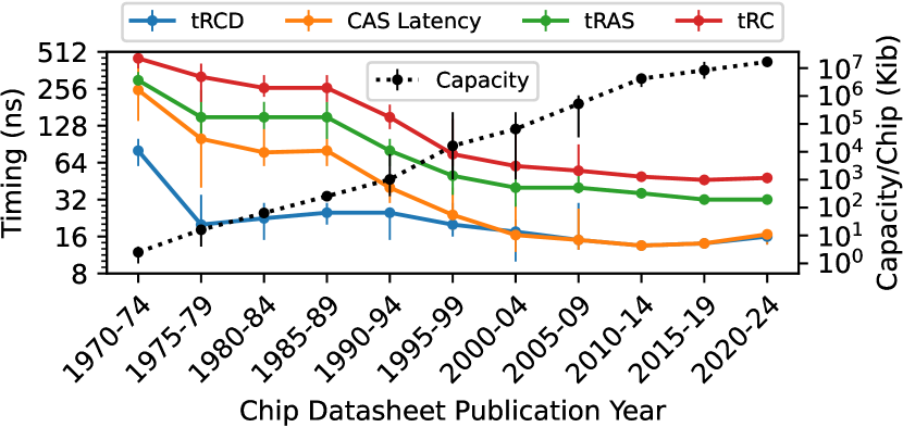
Parameter Definition tRCD minimum row activation to column operation delay CAS Latency read operation to data access latency tRAS minimum row activation to precharge delay tRC minimum delay between accesses to different rows across each 5-year period of time.
We observe a clear trend that newer DRAM chips exhibit improvements in all four timing parameters and storage capacity. However, none of the four timings have improved significantly in the last two decades. For example, the median tRCD/CAS Latency/tRAS/tRC reduced by 2.66/3.11/2.89/2.89% per year on average between 1970 and 2000, but only 0.81/0.97/1.33/1.53% between 2000 and 2015.333We report 2015 instead of 2020 because 2020 shows a regression in CAS latency due to first-generation DDR5 chips, which we believe is not representative because of its immature technology. In contrast, storage capacity improved relatively consistently with an exponential growth factor of 0.328 per year (0.341 for 1970-2000 and 0.278 for 2000-2020) across the entire history of DRAM technology. This data is consistent with similar studies done in prior work [36, 32, 37, 38, 39, 33, 40, 41, 42, 43], showing that commodity DRAM manufacturers have prioritized storage capacity over access latency in recent years.
Unfortunately, prioritizing storage density does not always align with the increasingly diverse needs of modern computing systems. These needs change as systems continuously evolve, so there is no single target metric (e.g., storage capacity) that suits all DRAM-based systems. Instead, each system’s design goals differ based on factors such as cost, complexity, applications, etc. For example, storage-focused data centers (e.g., content delivery network nodes) may require high-reliability memory while compute-focused clusters may optimize for performance with low-latency memory. Unfortunately, system designers today are limited to a narrow range of commodity DRAM products,444Custom DRAM chips (e.g., latency-optimized [44, 45], high-reliability [46, 47]) and target-specific chips (e.g., LPDDRn [14, 15], GDDRn [16, 17]) sacrifice the cost advantages of high-volume general-purpose commodity DRAM [20]. that effectively restrict design freedom and limit the peak potential of DRAM-based systems.
To address this disparity, system designers have long since developed techniques for adapting unmodified commodity DRAM chips to varying system requirements. Examples include: (1) actively identifying and/or mitigating errors to improve reliability [48, 49, 50, 51, 52, 53, 54, 55, 56, 57, 58, 59, 60, 61, 62, 63, 64, 65]; (2) exploiting available timing [66, 39, 67, 68, 69, 70, 71, 72] and voltage [73, 74, 75] margins to reduce memory access latency, power consumption, decrease refresh overheads [76, 77, 22, 78, 79, 80, 81, 82, 78]; and (3) mitigating unwanted DRAM data persistence [83, 84, 85] and read-disturb problems [86, 87, 88, 89, 90]. Section 2.1 discusses these proposals in greater detail to motivate the need to adapt commodity DRAM to diverse yet aggressive design targets.
However, these proposals are largely theoretical ideas or proofs-of-concept based on performance and reliability characteristics that are assumed, inferred, or reverse-engineered from a limited set of observations and DRAM products (e.g., in-house experimental studies) without DRAM manufacturers’ support. Therefore, adopting such proposals in a consumer-facing product requires a system designer to weigh the benefits of enhancing DRAM (e.g., improving performance, security, etc.) against both: (1) risks (e.g., failures in the field) associated with potentially violating manufacturer-recommended operating conditions and (2) limitations due to compatibility with only a subset of all commodity DRAM products (e.g., only those that have been accurately reverse-engineered). These risks and limitations are a serious barrier to adoption, especially for small-scale designers who may have limited headroom and expertise for exploring unconventional designs.
In this work, we argue that the lack of transparency concerning DRAM reliability characteristics is ultimately responsible for confining system designers to conventional, specification-constrained designs. For example, safely improving DRAM access latency by adjusting operating timings requires understanding the possible failure modes resulting from using non-standard timings (discussed further in Section 6). This is because selecting suitable operating timings requires the system designer to estimate the reliability impact of the new timings, which in turn requires reliability modeling or extensive testing under worst-case operating conditions. Unfortunately, obtaining the information necessary to make these estimates (e.g., error models, worst-case testing parameters) is difficult, if not impossible,555For all but the largest customers capable of independently conducting rigorous post-manufacturing testing. without transparency from DRAM manufacturers. This transparency does not exist today, even through private agreements for high-volume consumers who have significant stake in the DRAM industry [91, 92, 93]. In general, without the ability to understand how different design choices can impact DRAM reliability (e.g., error rates), system designers are discouraged from deploying or even exploring alternative designs.
To understand the source of the transparency problem, we conduct four case studies throughout Sections 4–7 that each examine a key system design concern for commodity DRAM chips: (1) reliability; (2) refresh overheads; (3) access latency; and (4) the RowHammer security vulnerability. For each case study, we explain how system designers are forced to make assumptions about DRAM reliability in order to address these concerns without breaking design independence with DRAM manufacturers, but those very assumptions limit the practicality and scope of the solution. We then argue that DRAM standards lie at the heart of the problem because they do not adequately address the aforementioned DRAM reliability concerns. To overcome this reliance on assumptions, we show that incorporating specifications for consumer-visible DRAM reliability characteristics (e.g., industry-validated error models and testing techniques) into DRAM standards alleviates the problem and allows system designers to better adapt commodity DRAM to their particular needs without requiring changes to how DRAM manufacturers design and build commodity DRAM.
We propose incorporating information transparency into DRAM standards using a two-step approach involving all DRAM stakeholders, including consumers and manufacturers. In Step 1, for DRAM chips already in the field, we seek the release of basic information about DRAM chips that consumers can use to better understand the chips’ reliability characteristics. Section 9.1 details examples of possible information to release, including (1) basic microarchitectural characteristics (e.g., organization of physical rows, sizes of internal storage arrays) that can be reverse-engineered using existing techniques with access to appropriate testing infrastructure [94, 68, 95, 39, 96, 97, 98, 67, 99, 100] and (2) industry-recommended testing best practices (e.g., test patterns for key error mechanisms). We believe that this information can be released through a combination of (1) crowdsourced testing of commodity DRAM chips on the market; and (2) DRAM chip manufacturers publishing information (e.g., using datasheet revisions or online resources) about their products, possibly limited to basic information that manufacturers already have available (i.e., that requires minimal logistical effort to release). Through a combination of these two avenues, information can be provided to all system designers, including the majority of designers without the ability to conduct exhaustive testing, almost immediately without requiring changes to existing DRAM hardware or standards (though standardizing the information release could streamline the process). Then, armed with this information, system designers can make more informed decisions when developing their own solutions to system-specific design concerns while also preserving the advantages of commodity DRAM built per general-purpose DRAM standards.
In Step 2, we propose extending DRAM standards with explicit DRAM reliability standards that provide industry-standard guarantees, tools, and/or information helpful to consumers. We envision different possibilities for these reliability standards, including (1) reliability guarantees for how a chip is expected to behave under certain operating conditions (e.g., predictable behavior of faults [101]); (2) disclosure of industry-validated DRAM reliability models and testing strategies suitable for commodity DRAM chips (e.g., similar to how JEDEC JEP122 [102], JESD218 [103], and JESD219 [104] address Flash-memory-specific error mechanisms [105, 106, 107] such as floating-gate data retention [108, 109, 110, 111] and models for physical phenomena such as threshold voltage distributions [112, 113, 114, 115]); and (3) requirements for manufacturers to directly provide relevant information about their DRAM chips (e.g., the information requested in Step 1). As the DRAM industry continues to evolve, we anticipate closer collaboration between DRAM and system designers to efficiently overcome the technology scaling challenges that DRAM is already facing [26, 28, 116, 117]. Although we hope that transparency will occur naturally as part of this process, we believe the end result will be determined in a large part by the direction in which DRAM standards evolve. Therefore, we believe that ensuring transparency of reliability characteristics becomes a first-order concern is essential for allowing innovation going forward.
We make the following contributions:
-
1.
We make a case for the DRAM industry to provide transparency into the consumer-visible reliability characteristics of commodity DRAM chips so that system designers can make informed decisions when integrating commodity chips into their designs.
-
2.
We support our argument with four case studies (DRAM reliability, DRAM refresh, DRAM access latency, and RowHammer), showing that system designers require insight into commodity DRAM chip reliability in order to adopt improvements in any of the four directions.
-
3.
We identify modern DRAM standards as the primary factor that limits system designers from comprehensively understanding the reliability impact of their design decisions, thereby discouraging the designers from adopting techniques to better adapt commodity DRAM chips to their systems’ specific needs.
-
4.
We propose a new two-step approach to facilitate transparency into consumer-visible DRAM reliability characteristics. In the short term, we ask for information release through a combination of both (1) crowdsourced testing from DRAM consumers; and (2) official information from DRAM manufacturers, possibly standardized by extensions to DRAM standards. In the long term, we propose extending DRAM standards with explicit DRAM reliability standards that provide industry-standard guarantees, tools, and/or information that enable DRAM consumers to perform their own reliability analyses and understand DRAM reliability at different operating points.
2 The System Designer’s Challenge
Today’s DRAM industry thrives on separation of concerns: DRAM manufacturers can focus on designing highly-optimized DRAM chips while consumers can make use of standardized DRAM that conform to JEDEC standards. This design independence is powerful because it allows each party to leverage their respective expertise to build the best possible product. As a result, a system designer who is responsible for choosing the memory substrate for a particular system can simply select between a limited range of standardized commodity parts that are optimized for different targets, such as general-purpose performance (e.g., DDRn [10, 11]), high bandwidth (e.g., GDDRn [16, 17], HBMn [12, 13]), and low power (e.g., LPDDRn [14, 15]).
Unfortunately, the system designer faces a significant challenge: the designer is unable to fully explore the memory design space (as well as the system-memory co-design space) because there are only a limited number of viable design points using commodity DRAM chips. Therefore, the limited number of options inherently forces the designer to overlook opportunities for customizing DRAM operation towards their system’s particular design goals. As main memory becomes an increasingly significant system bottleneck [116, 118, 119], we believe that enabling system designers to flexibly adapt commodity DRAM to suit their own needs as they see fit is a promising path to reap the benefits of adaptability while preserving the design independence between DRAM manufacturers and system designers.
2.1 Benefits for DRAM Consumers
Prior works [48, 49, 50, 51, 52, 53, 54, 55, 57, 58, 59, 60, 81, 120, 121, 76, 122, 123, 124, 77, 125, 126, 79, 22, 80, 82, 127, 128, 129, 130, 131, 132, 133, 134, 78, 135, 66, 39, 67, 68, 69, 70, 71, 136, 72, 135, 137, 138, 97, 139, 140, 141, 142, 143, 144, 145, 146, 147, 86, 148, 149, 87, 150, 151, 152, 90] demonstrate significant system-level benefits from adapting commodity DRAM operation to different system needs without changing the DRAM design itself. This section reviews the benefits of four concrete examples of such customizations: 1) DRAM reliability improvement, 2) DRAM refresh overhead reduction, 3) DRAM access latency reduction, and 4) RowHammer security improvement. In principle, a system designer can readily implement each customization using existing techniques. Unfortunately, adopting these techniques in practice requires understanding how DRAM reliability characteristics behave under different operating conditions, which is not clearly communicated by DRAM manufacturers or standards today. In this section, we review each example customization’s potential benefits; then, our case studies throughout Sections 4-7 explore each example customization in further detail to identify the specific factors that we believe discourage system designers from adopting the examples in practice.
2.1.1 DRAM Reliability Improvement
DRAM is susceptible to a wide variety of error mechanisms that can impact overall system reliability. To combat DRAM-related failures, system designers typically incorporate reliability, availability and serviceability (RAS) features [153, 154, 155] that collectively improve system reliability beyond what commodity DRAM chips can provide alone. In general, memory RAS is a broad research area with solutions spanning the hardware-software stack, ranging from hardware-based mechanisms within the DRAM chip (e.g., on-die ECC scrubbing [11, 156, 101], post-package repair [157, 10, 11, 158, 159], target row refresh [100, 160]), memory controller (e.g., rank-level ECC [48, 49, 50, 51, 52, 53, 54, 55, 57, 58, 59, 60, 81], rank-level ECC scrubbing [56, 82, 61, 62, 63, 64, 65, 161, 156, 62], repair techniques [79, 22, 162, 163, 164, 165, 166, 167, 168, 169]) to software-only solutions (e.g., page retirement [120, 121, 76, 122, 123, 124], failure prediction [170, 171, 172, 173, 174, 175]).
As a specific and relevant example, an important category of hardware-based redundancy mechanisms known as rank-level error-correcting codes (rank-level ECC) operate within the memory controller to isolate the rest of the system from random DRAM errors. Depending on the ECC design, rank-level ECC can protect against random single-bit (e.g., SEC/SEC-DED Hamming codes [176]), multi-bit (e.g., BCH [177, 178], Reed-Solomon [179]), and/or multi-component (e.g., Chipkill [19, 48]) errors with varying hardware and runtime overheads. The system designer must decide which ECC mechanism is most appropriate for their particular system (e.g., which error mechanisms are dominant and what degree of protection is required). For example, a state-of-the-art rank-level ECC mechanism called Frugal-ECC [53] uses data compression to provide chipkill-correct ECC for 4 non-ECC DIMMs and 8 ECC DIMMs with negligible performance (maximum of 3.8%), energy-efficiency, and area overheads compared with an industry-standard chipkill solution. Therefore, Frugal-ECC enables system designers to implement chipkill reliability using commodity DRAM chips with a fraction of the storage overheads suffered by conventional ECC DIMM configurations.
2.1.2 DRAM Refresh Overhead Reduction
DRAM stores data in volatile capacitors, which are susceptible to charge leakage. To prevent this leakage from causing data loss, DRAM requires periodic refresh operations that intermittently access all DRAM cells to restore their charge levels to safe values. Unfortunately, DRAM refresh operations are well known to waste significant system performance and power [125, 132, 180, 77, 22, 181, 126, 122, 135, 182], sacrificing almost half of the total memory throughput and wasting almost half of the total DRAM power for projected 64 Gb chips [77].
To alleviate the power and performance costs of DRAM refresh, prior works [77, 125, 126, 76, 79, 22, 80, 82, 127, 128, 129, 130, 131, 132, 133, 134, 78, 135] take advantage of the fact that most refresh operations are unnecessary.666Latency-hiding techniques (e.g, prefetching, memory command scheduling, on-chip caching, etc.) and parallelization of refresh and access operations [183, 43, 184, 185, 186] help mitigate performance overheads but do not change the total number of refresh operations issued. As a result, such techniques cannot mitigate energy wastage due to DRAM refresh. These techniques are also imperfect in many cases where latency-hiding is impractical (e.g., row conflicts between refresh and access commands, larger memory footprints than available caching resources) [187, 184, 188, 183]. The standard DRAM refresh algorithm refreshes all cells frequently (i.e., at the worst-case rate) to simplify DRAM refresh and guarantee correctness. However, each cell’s data retention characteristics vary significantly due to a combination of data-dependence [129, 130, 189, 127, 78] and process variation [190, 191, 23, 22, 189, 77, 126]. As a result, eliminating unnecessary refresh operations can provide significant power reduction and performance improvement. For example, Liu et al. [77] demonstrate an average energy-per-access and system performance improvement of 8.3% and 4.1%, respectively, for 4 Gib chips (49.7% and 107.9% for 64 Gib chips) when relaxing the refresh rate at the row granularity. Therefore, reducing refresh overheads can potentially benefit any DRAM-based system.
2.1.3 DRAM Access Latency Reduction
Figure 2 shows that DRAM access latency has not significantly improved relative to storage capacity over the last two decades. This makes DRAM an increasingly significant system performance bottleneck today, especially for workloads with large footprints that are sensitive to DRAM access latency [192, 193, 194, 195, 196, 197, 198, 199, 200, 72, 201, 36, 116, 202, 203, 204, 205, 206, 118, 207, 208, 209, 210, 211, 212]. Although conventional latency-hiding techniques (e.g., caching, prefetching, multithreading) can potentially help mitigate many of the performance concerns, these techniques (1) fundamentally do not change the latency of each memory access and (2) fail to work in many cases (e.g., irregular memory access patterns, random accesses, huge memory footprints).
To address this problem, prior works have taken two major directions. First, many works [66, 39, 67, 68, 69, 70, 71, 136, 72, 135, 137] show that the average DRAM access latency can be shortened by reducing DRAM access timings for particular memory locations that can tolerate faster accesses. This can be done safely because, although DRAM standards call for constant access timings across all memory locations, the minimum viable access timings that the hardware can support actually differ between memory locations due to factors such as heterogeneity in the circuit design [69, 33] and manufacturing process variation between circuit components [66, 39, 67, 73, 68].
Exploiting these variations in access timings to reduce the average memory access latency can provide significant system performance improvement. For example, Chang et al. [39] experimentally show that exploiting access latency variations can provide an average 8-core system performance improvement of 13.3%/17.6%/19.5% for real DRAM chips from three major DRAM manufacturers. Similarly, Kim et al. [67] show that exploiting access latency variations induced by DRAM sense amplifiers provides an average (maximum) system performance improvement of 4.97% (8.79%) versus using default DRAM access timings for 4-core heterogeneous workload mixes based on data obtained from 282 commodity LPDDR4 DRAM chips.
Second, other works [138, 97, 139, 140, 141, 142, 143, 144, 145, 146, 147] show that commodity DRAM can perform massively-parallel computations (e.g., at the granularity of an 8 KiB DRAM row) by exploiting the underlying analog behavior of DRAM operations (e.g., charge sharing between cells). These works show that such computations can significantly improve overall system performance and energy-efficiency by both (1) reducing the amount of data transferred between the processor and DRAM and (2) exploiting the relatively high throughput of row-granularity operations. For example, Gao et al. [138] show that in-DRAM 8-bit vector addition is more energy-efficient than the same computation in the processor, primarily due to avoiding the need for off-chip data transfers. Similarly, Olgun et al. [139] use an end-to-end FPGA-based evaluation infrastructure to demonstrate that in-DRAM copy and initialization techniques can improve the performance of system-level copy and initialization by and , respectively.
2.1.4 Improving Security Against RowHammer
RowHammer [87, 213, 214, 215] is a well-studied read-disturb phenomenon in modern DRAM chips in which memory accesses to a given memory location can induce bit-flips at other locations. Recent experimental studies [87, 216] show that RowHammer is continually worsening with process technology shrinkage. Although DRAM manufacturers incorporate internal RowHammer-mitigation mechanisms [217, 218, 160, 100, 219, 216, 220], prior work [160, 221, 100, 222, 217] shows that these mechanisms do not suffice. Therefore, several works [86, 223, 87, 224, 225, 88] provide RowHammer-mitigation mechanisms that operate from outside of the DRAM chip to provide strong security without requiring changes to DRAM chip hardware or relying upon information from DRAM manufacturers. Such a solution is attractive for a system designer with interest in building a secure system because the designer can rely upon their own methods rather than relying upon external, possibly difficult-to-verify promises or guarantees [92, 226].
Following prior work [86], we classify previously-proposed RowHammer defenses into four different categories as follows.
-
1.
Access-agnostic mitigation hardens a DRAM chip against RowHammer independently of the memory access pattern. This includes increasing the overall DRAM refresh rate [87, 88, 225] and memory-wide error correction and/or integrity-checking mechanisms such as strong ECC [226, 219, 87]. These mechanisms are algorithmically simple but can introduce significant system hardware, performance, and/or energy-efficiency overheads (e.g., a large number of additional refresh operations [87, 216, 182]).
- 2.
- 3.
- 4.
RowHammer defense is an ongoing area of research, and which mechanism type is most effective depends on the level of security (e.g., the threat model) that the system designer requires and the trade-offs (e.g., performance, energy, hardware area, complexity overheads) they are willing to make.
2.2 Benefits for DRAM Manufacturers
We believe that the ability to adapt commodity DRAM to system-specific design goals also benefits DRAM manufacturers for two key reasons. First, adaptability broadens the scope and competitive advantage of DRAM technology relative to alternative technologies (e.g., emerging memories). Second, enabling DRAM consumers to more easily innovate on the DRAM substrate can encourage valuable feedback for DRAM manufacturers, including insights from customer use-cases and well-evaluated suggestions for future products.
Regardless of these benefits, we believe making commodity DRAM adaptable has no significant downside for DRAM manufacturers. The reliability characteristics that we wish to be communicated (as described in detail in Section 9.1) are either (1) already exposed in scientific studies today; or (2) can be reverse-engineered using existing techniques by those with access to appropriate tools (e.g., competitors, scientific labs). We simply ask for these characteristics to be officially provided in a trustworthy capacity. DRAM manufacturers have not previously provided this information because there has been no pressing need to do so. However, releasing this information makes sense today because it can enable a broad range of benefits for DRAM consumers going forward, especially as DRAM technology scaling continues to face increasing difficulties [116, 241, 214].
2.3 Short-Term vs. Long-Term Solutions
Prior works [242, 118, 241, 116, 87, 26, 214, 215] have praised the merits of cooperation between DRAM manufacturers and system designers in order to collaboratively solve main memory challenges across the system stack. However, this requires either (1) breaking design independence between the two parties; (2) achieving consensus among all DRAM stakeholders (i.e., JEDEC committee members and representatives, including DRAM manufacturers and consumers) for every design change, followed by a lengthy adoption period; or (3) reducing dependence on DRAM standards and JEDEC. We do not believe any of these options are easy to adopt for either the (1) short term, where we would like to quickly effect changes that enable information transparency; or (2) long term, where breaking design independence constrains the very freedom that we advocate system designers should have in meeting their own design goals while preserving the cost advantages of mass-produced commodity DRAM chips.
Instead, we argue for enabling each party to solve their own system-specific design challenges, modifying DRAM standards only for issues that collectively affect all DRAM stakeholders. However, regardless of how the DRAM industry evolves over the coming years, we firmly believe that DRAM must become more adaptable, whether that occurs through standards or collaboration.
3 Quantitatively Measuring Reliability
As we will show in the following case studies (Sections 4–7), a system designer exploring unconventional DRAM operating points must first understand how reliably a chip will behave at that operating point. Given that this behavior is not governed by DRAM standards or described by DRAM manufacturers, the system designer must determine it themselves, e.g., through modeling and/or testing. This section formalizes the information that a system designer may need (but does not necessarily have access to today) in order to quantitatively understand DRAM reliability.
3.1 Information Flow During Testing
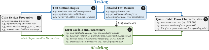
Figure 2 describes the flow of information necessary for a system designer to quantitatively estimate777“Estimate” because, in general, no model or experiment is likely to be perfect, including those provided by manufacturers. a DRAM chip’s error characteristics starting from basic properties of the chip . In principle, these characteristics can comprise any aspect of DRAM reliability that a system designer wants to quantify while exploring their system’s design and/or configuration space. Examples include: (1) worst-case error rates (e.g., bit error rate (BER) or failures in time (FIT)) across a given set of operating points; (2) a profile of error-prone memory locations; or (3) a list of error-free operating points (e.g., as identified in a shmoo analysis [243]). The error characteristics can be estimated in two different ways: testing or modeling.
3.1.1 Determination from Testing
First, a system designer may estimate error characteristics using measurements from detailed experimental testing across a variety of operating conditions. Examples of measured quantities include: aggregate error rates, per-cell probabilities of error, and spatial/temporal error distributions. These measurements can be made using testing infrastructures ranging from industry-standard large-scale testing equipment [244, 245] to home-grown tools based on commodity FPGAs [246, 139, 247, 87, 138, 73, 34, 248, 39, 127, 249, 250] or DRAM-based computing systems [251, 221, 252, 253, 74].
To conduct accurate and rigorous testing, the system designer must use an effective test methodology that suits the particular DRAM chip under test. Prior works extensively study key aspects of effective test methodologies, including appropriate data and access patterns, the effects of enabling/disabling DRAM chip features such as target row refresh (TRR) [160, 239, 100, 222, 216] and on-die error correcting codes (on-die ECC) [54, 28, 26, 254, 23, 30, 255, 256, 257, 95, 258, 259], and the viability of different DRAM command sequences (e.g., sequences that enable in-DRAM row copy operations [142, 138, 139, 260], true random-number generation [140, 141, 261, 262], and physically unclonable functions [97, 263]).
In turn, choosing an effective test methodology requires knowledge of basic properties about a DRAM chip’s design and/or error mechanisms . For example, DRAM manufacturer’s design choices for the sizes of internal storage arrays (i.e., mats [69, 264, 36, 140]), charge encoding conventions of each cell (i.e., the true- and anti-cell organization [98, 189]), use of on-die reliability-improving mechanisms (e.g., on-die ECC, TRR), and organization of row and column addresses all play key roles in determining if and how susceptible a DRAM chip is to key error mechanisms (e.g., data retention [191, 98, 95, 189, 265, 266, 267], access-latency-related failures [67, 37, 68, 69, 39, 140, 72, 66], and RowHammer [87, 214, 215, 268, 269, 270]). Section 9.1.1 provides further detail about such design properties and how knowing them is necessary to develop effective test methodologies.
3.1.2 Determination from Modeling
Second, the system designer may make predictions from analytical or empirical error models based on a previous understanding of DRAM errors (e.g., from past experiments or scientific studies). Examples of such error models include: analytical models based on understanding DRAM failure modes (e.g., sources of runtime faults [21, 271, 49, 123, 272, 273]), parametric statistical models that provide useful summary statistics (e.g., lognormal distribution of cell data-retention times [190, 191, 274, 275, 276, 277, 278, 279, 280], exponential distribution of the time-in-state of cells susceptible to variable-retention time (VRT) [265, 281, 82, 282, 283, 284, 285, 286, 287, 288, 289, 127, 26, 189]), physics-based simulation models (e.g., TCAD [269, 290, 291, 292, 274] and SPICE models [293, 227, 69, 136, 37, 294, 70, 71, 295]), and empirically-determined curves that predict observations well (e.g., single-bit error rates [78, 82, 189, 127, 129, 270]). Similar to testing, using error models to predict error characteristics ultimately relies on understanding the DRAM chip being tested because the accuracy of the predictions requires choosing appropriate models and model parameters (e.g., through testing or directly from fundamental chip design properties ).
3.2 Access to Modeling and Testing Information
Figure 2 shows that determining a DRAM chip’s error characteristics through modeling or testing ultimately relies on understanding the chip’s fundamental design properties. This reliance can be implicit (e.g., inherent within a pre-existing workflow designed for a specific chip) or explicit (e.g., chosen as part of a home-grown testing methodology). Therefore, a system designer must be vigilant of the information they (perhaps unknowingly) rely upon at each step of their design process concerning commodity DRAM.
Fortunately, the system designer only needs to be concerned with the information flow at the children of a node whose information is already known from a trustworthy source. For example, a system designer who wants to identify the locations of error-prone cells (i.e., ) using testing need not be concerned with chip design properties (i.e., ) if DRAM manufacturers provide appropriate test methodologies (i.e., ) or detailed test results (i.e., ). Unfortunately, to our knowledge, neither DRAM standards nor manufacturers provide the information in any of the nodes today, much less in a clear, industry-validated manner. Therefore, the system designer lacks a base of trustworthy information to build upon. This creates a barrier to entry for a system designer who wants to explore optimizations to commodity DRAM by compromising the designer’s ability to make well-informed or effective decisions.
In general, except for the few major DRAM customers who may be able to secure confidentiality agreements,888Even under confidentiality, DRAM manufacturers may be unwilling to reveal certain proprietary aspects of their designs (e.g., on-die error correction [258, 296], target row refresh [92]) or provide specifically requested numbers. system designers would need to rely on (possibly incorrect or incomplete) inferences or assumptions based on domain knowledge or reverse-engineering studies (e.g., similar in spirit to [78, 98, 189, 258, 216, 94, 297, 100, 298, 160, 299, 300, 301, 67, 39, 69]) that are not verified or supported by the DRAM industry.999DRAM manufacturers may make assumptions during their own testing. However, they have full transparency into their own designs (i.e, the root node in the information flow), so they can make the most informed decision. As a result, the need for assumptions can discourage practitioners from exploring the full design space even when a given design choice is otherwise beneficial. We conclude that the lack of information transparency is a serious impediment to adopting many promising DRAM-related optimizations today.
4 Study 1: Improving Memory Reliability
Main memory reliability is a key design concern for any system because when and how memory errors occur affects overall system reliability. In particular, designers of reliability-critical systems such as enterprise-class computing clusters (e.g., cloud, HPC) and systems operating in extreme or hostile environments (e.g., military, automotive, industrial, extraterrestrial) take additional measures (e.g., custom components [302, 46, 47, 303, 304, 305, 306, 307, 308], redundant resources [309, 310, 60]) to ensure that memory errors do not compromise their systems. Section 2.1.1 shows the benefits of incorporating mechanisms to improve memory reliability. This section explains how the details of a DRAM chip’s reliability characteristics play a major role in determining how system designers improve overall system reliability.
4.1 Adapting Commodity DRAM Chips
Commodity DRAM is designed to work for a wide variety of systems at a reasonable (albeit unspecified)101010Academic works speculate that commodity DRAM targets a bit error rate (BER) within the range of [22, 311, 163, 78], but we are unaware of industry-provided values. error rate. In general, a system designer who needs high memory reliability must design and build their own solutions (i.e., outside of the DRAM chip) to tolerate memory errors.111111Even designers who adopt custom DRAM solutions that sacrifice the cost advantages of commodity memory (e.g., high-reliability DRAM [46, 47]) may supplement the DRAM chips with additional error-mitigation mechanisms outside of the DRAM chip. In doing so, the designer effectively adapts a DRAM chip to specific system needs, enhancing DRAM reliability beyond what the DRAM chips provide alone.
Section 2.1.1 reviews examples of such memory error-mitigation mechanisms, which span the hardware-software stack. Regardless of where each mechanism operates from, the mechanism targets a particular error model, which defines the scope of the errors that it is designed to mitigate. This is important because, while a given mechanism efficiently mitigates errors within its target error model, it may fail to do so if errors no longer fit the model. In such cases, a different error-mitigation mechanism (or possibly, a combination of multiple mechanisms) may be more suitable.
For example, a coarse-grained approach such as page retirement [120, 121, 76, 122, 123, 124] efficiently mitigates a small number of errors at fixed bit positions. However, page retirement exhibits significant capacity and performance overheads at high error rates or when mitigating errors that change positions over time [124, 312, 120]. In contrast, a fine-grained hardware-based approach such as a block error-correcting code [313, 314, 315, 316, 317, 318] can efficiently mitigate a limited number of randomly-distributed errors but can fail silently (and even exacerbate the number of errors present [319, 320, 101, 30, 95, 258, 259]) when its correction capability is exceeded. We conclude that it is essential for the system designer to know when and how errors occur in a given memory chip in order to make an informed choice of which error-mitigation mechanism to use in a particular system.
4.2 Lack of Transparency in Commodity DRAM
Unfortunately, system designers generally do not have access to definitive error models for commodity DRAM chips. Therefore, designers are left to rely upon information they can gather by themselves (e.g., by expending testing resources) or from external, possibly untrustworthy, sources. However, as Section 3 discusses, obtaining the error characteristics of a DRAM chip without input from the manufacturers requires making a series of assumptions about the chip’s design and testing methodologies. The need for these assumptions (i.e., the lack of trustworthy information) can easily discourage designers from pursuing custom solutions to enhance DRAM reliability.
To exacerbate the problem of identifying a definitive error model, DRAM manufacturers are starting to incorporate two on-die error-mitigation mechanisms that correct a limited number of errors from within the DRAM chip itself: (1) on-die ECC [28, 54, 255, 256, 257, 254, 95, 258] for improving reliability and yield and (2) target row refresh [100, 160, 222, 239] for partially mitigating the RowHammer vulnerability. Prior works on ECC [30, 321, 54, 320, 27, 322, 101, 323, 296, 95, 258, 324, 259] and RowHammer [92, 226, 160, 100] show that both on-die ECC and TRR change how errors appear outside of the DRAM chip, thereby changing the DRAM error model seen by the memory controller (and therefore, to the rest of the system). Unfortunately, both mechanisms are opaque to the memory controller and are considered trade secrets that DRAM manufacturers will not officially disclose [23, 22, 95, 258, 92, 226, 93, 298]. As a result, both on-die ECC and TRR make it difficult for a system designer to reason about the DRAM error model and error rates. For example, to account for on-die ECC’s and TRR’s effects when designing a system-level error-mitigation mechanism, the system designer must spend additional time and resources using reverse-engineering techniques (e.g., for on-die ECC [95, 258] or TRR [100, 160]) or otherwise find a trustworthy source to acquire the necessary information in reliable manner.
5 Study 2: DRAM Refresh Overheads
DRAM refresh is a key design concern in modern systems. Section 2.1.2 reviews evidence that reducing the total number of refresh operations significantly benefits overall system performance and energy efficiency. In this section, we examine how mitigating refresh overheads in commodity DRAM requires making assumptions about DRAM reliability characteristics. Based on our analysis, we argue that these assumptions limit the techniques’ potential for adoption, discouraging system designers from using these solutions in practice.
5.1 Adapting Commodity DRAM Chips
Reducing unnecessary refresh operations in commodity DRAM chips generally requires two key steps. First, the memory controller must reduce the frequency of periodic refresh operations. This is achievable (though not necessarily supported to arbitrary values) using commodity DRAM chips because the memory controller manages DRAM refresh timings. For example, the memory controller might relax the rate at which it issues refresh operations to half of the DDRn standard of 3.9 or 7.8 s, which is supported by standards at extended temperature ranges [11, 15, 14, 10, 9], or even to over an order of magnitude less often [76, 77, 22, 134].
Second, the system must mitigate any errors that may occur within the small number of DRAM cells that require frequent refreshing. Doing so requires either using additional refresh operations (e.g., by issuing extra row activations [77]) or using error-mitigation mechanisms within processor (e.g., ECC [82] and/or bit-repair techniques [76, 79, 22]). Although both strategies introduce new performance and energy overheads, the benefits of reducing unnecessary refresh operations outweigh the overheads introduced [77, 125, 126, 76, 79, 22, 80, 82, 78, 325]. For example, Liu et al. [77] project that DRAM refresh overheads cause a 187.6% increase in the energy-per access and a 63.7% system performance degradation for 64 Gib chips. By reducing the overall number of DRAM refresh operations, the authors show that their mechanism, RAIDR, can mitigate these overheads by 49.7% and 107.9%, respectively.
5.2 Lack of Transparency in Commodity DRAM
Knowing, predicting, or identifying cells that cannot safely withstand infrequent refreshing (i.e., retention-weak cells) is a difficult reliability problem because the cells’ likelihood of error changes with how a DRAM chip is used (i.e., operating conditions such as the refresh rate, voltage, temperature) and the particular DRAM chip circuit design (e.g., random cell-to-cell variations, locations of true and anti-cells [189, 98, 95]). Prior works propose two practical ways of identifying retention-weak cells: (1) active profiling, which uses comprehensive tests to search for error-prone cells offline [77, 78, 129, 127, 79, 135], and (2) reactive profiling, which constantly monitors memory to identify errors as they manifest during runtime, e.g., ECC scrubbing [82, 56, 61]. Both approaches require the profiler to understand the worst-case behavior of data-retention errors for a given DRAM chip [127, 79]: an active profiler must use the worst-case conditions to maximize the proportion of retention-weak cells it identifies during profiling [78] and a reactive profiler must be provisioned to identify (and possibly also mitigate) the worst-case error pattern(s) that might be observed at runtime, e.g., to choose an appropriate ECC detection and correction capability [324, 226, 127].
The fact that an effective error profiling mechanism relies on understanding the underlying error characteristics reinforces the argument presented in Section 3. Even though there exist techniques for mitigating refresh overheads in commodity DRAM, practically adopting them relies on prerequisite knowledge about a DRAM chip and its reliability characteristics that is not provided by the DRAM industry today.
6 Study 3: Long DRAM Access Latency
Slow generational improvements in the DRAM access latency (shown in Section 1) contrast with the growing prevalence of latency-sensitive workloads today [192, 193, 194, 195, 196, 197, 198, 199, 200, 72, 201, 36, 116, 202, 203, 204, 205, 206, 118, 207, 208, 209, 210, 211, 212, 326, 327, 328]. Therefore, as Section 2.1.3 discusses, there is significant opportunity for improving overall system performance by reducing the memory access latency [66, 39, 67, 68, 69, 70, 71, 136, 72, 135, 137, 329, 330]. In this section, we study how techniques for reducing the access latency of commodity DRAM chips rely on making assumptions about DRAM reliability characteristics. Then, we argue that the need for these assumptions (and the lack of transparency in DRAM to allow them) discourages system designers from adopting the latency reduction techniques.
6.1 Adapting Commodity DRAM Chips
Strategies for improving the access latency of commodity DRAM chips rely on manipulating DRAM commands and/or access timings to either (1) eliminate conservative timing margins that DRAM manufacturers use to account for worst-case operation [39, 68, 66, 135, 211, 67, 136, 74, 75, 137]; or (2) exploit undefined DRAM chip behavior to perform beneficial operations (e.g., performing massively-parallel computations within DRAM rows [146, 138, 142, 139, 144, 331, 143, 147, 332], generating random values [141, 261, 140] or unique chip identifiers [97, 263, 333, 334, 335]).
In both cases, new DRAM access timings must be determined that ensure the desired operation can be performed predictably and reliably under all conditions. To identify these access timings, prior works [97, 141, 336, 138, 140, 39, 73, 68, 66, 34, 246, 32, 33, 74] perform extensive experimental characterization studies across many DRAM chips. These studies account for three primary sources of variation that affect the access timings of a given memory location. First, process variation introduces random variations between DRAM chip components (e.g., cells, rows, columns). Second, a manufacturer’s particular circuit design introduces structural variation (called design-induced variation [69]) that deterministically affects access timings based on a component’s location in the overall DRAM design (e.g., cells along the same bitline [67], cells at the borders of internal storage arrays [69]). Third, the charge level of a DRAM cell varies over time due to leakage and the effects of DRAM accesses [211, 136]. Experimentally determining the new predictable and reliable access timings requires properly accounting for all three sources of variation under all operating conditions.
6.2 Lack of Transparency in Commodity DRAM
Unfortunately, determining new viable access timings requires developing and executing a reliable testing methodology, which in turn requires making similar assumptions to those discussed for data-retention error profiling in Section 5.2. Choosing runtime (e.g., data and access patterns) and environmental (e.g., temperature, voltage) testing conditions in a meaningful way requires some understanding of the error mechanisms involved in timing-related errors [130], including (but not limited to) aspects of the circuit design, such as internal substructure dimensions (e.g., subarray sizing) [67, 69], the correspondence between logical DRAM bus addresses and physical cell locations [39, 68, 129], and the order of rows refreshed by each auto-refresh operation [211]. A system designer is discouraged from exploring improvements to the commodity DRAM access latency without trustworthy access to this information.
7 Study 4: RowHammer Mitigation
Many promising proposals exist for adding RowHammer defenses to commodity DRAM chips (discussed in Section 2.1.4), but their potential for adoption is hampered by system designers’ lack of visibility into how the underlying error mechanism behaves. In this section, we examine the various assumptions that RowHammer defense proposals rely upon and argue that these assumptions pose serious barriers for practical adoption.
7.1 Adapting Commodity DRAM Chips
To effectively mitigate RowHammer bit flips, a mitigation mechanism must be configured based on the vulnerability level of a given DRAM chip. This requires estimating the chip’s RowHammer error characteristics for different operating conditions and access patterns. Each of the four mechanism types introduced in Section 2.1.4 requires estimating different characteristics. Table 1 summarizes the different pieces of information required for each mitigation type. The first is known as [216, 99] or RowHammer Threshold [87, 86, 337], which describes the worst-case number of RowHammer memory accesses required to induce a bit-flip. The second is known as the blast radius [87, 216], which describes how many rows are affected by hammering a single row. The third is the DRAM’s internal physical row address mapping [87, 338], which is necessary to identify the locations of victim rows.
| Required Information | |||
|---|---|---|---|
| Strategy | Blast Radius | Row Mapping | |
| Access-Agnostic | ✓ | ||
| Proactive | ✓ | ✓ | |
| Physically Isolating | ✓ | ✓ | ✓ |
| Reactive | ✓ | ✓ | ✓ |
All three RowHammer error characteristics vary between DRAM manufacturers, chips, and cells based on a combination of random process variation, a manufacturers’ particular circuit design (including yield-management techniques such as post-manufacturing repair, target row refresh, and error correcting codes), and operating conditions such as temperature and voltage [87, 270, 339, 216, 99, 224, 340, 341, 298]. Therefore, as with estimating DRAM refresh and access timings (discussed in Sections 5.2 and 6.2), these studies rely on extensive experimental testing to estimate RowHammer error characteristics that are needed to design and/or configure the RowHammer defenses discussed in Section 2.1.4.
7.2 Lack of Transparency in Commodity DRAM
We observe that all previously-proposed RowHammer mitigation mechanisms require accurately estimating RowHammer error characteristics throughout all valid operating conditions. In particular, every mechanism must be tuned against at least in order to effectively prevent RowHammer. Prior works [226, 92, 93] make the same observation, discussing the difficulty in practically determining and relying on this information without support from DRAM manufacturers.
Therefore, a security-focused system designer who wants to implement or build upon one of the many previously-proposed system-level RowHammer defense mechanisms (discussed in Section 2.1.4) is limited by the same information access challenges as discussed in Section 3.2: because neither the error characteristics they need nor the methods to obtain them are provided by official sources, the system designer must rely on other means to obtain the necessary information. As a result, the system designer is likely discouraged from exploring designs that address RowHammer errors in commodity DRAM chips altogether.
8 Current DRAM Standards as the Problem
Based on our case studies, we conclude that reliance on information about DRAM reliability characteristics poses a serious challenge for optimizing how commodity DRAM is used. In this section, we hypothesize that the unavailability of information related to DRAM reliability is caused by a lack of transparency within DRAM standards which provide control over, but not insight into, DRAM operations. We identify DRAM standards as both (1) the root cause of having to make assumptions about DRAM reliability (as standards are currently defined) and (2) the pathway to a solution for alleviating the need for such assumptions (by incorporating DRAM reliability as a key concern).
8.1 The Problem of Information Unavailability
In each case study throughout Sections 4–7, we observe that optimizing commodity DRAM chips for key system design concerns requires knowing information about DRAM reliability. This is unsurprising because reliability is central to each case study’s approach: each study improves system-level metrics (e.g., reliability, energy-efficiency, performance, security) by leveraging key properties of one or more error mechanisms (e.g., spatiotemporal dependence of errors due to circuit timing violations [67, 39, 69], the localized nature of RowHammer errors [87, 150, 151, 152, 216]). Therefore, identifying the best operating point requires at least a basic understanding of how the error mechanisms themselves behave under representative operating conditions.
Recent works [226, 92] discuss the pitfalls of designing defense mechanisms that rely on knowledge of how RowHammer errors behave (e.g., , dependence on a chip’s internal cell organization), calling into question the practicality of accurately determining these details given an arbitrary DRAM chip. Knowing or determining this information is essential to guarantee protection against RowHammer. However, determining it without guidance from DRAM manufacturers requires per-chip testing and/or reverse-engineering that relies on the accuracy of the underlying testing methodology used, which itself relies on knowledge of DRAM chip details that likely needs to be assumed or inferred (as discussed in Sections 3 and 7.2).
As a result, a system designer who wants to adapt commodity DRAM for their design requirements today is forced to make design and/or mechanism configuration decisions based upon assumptions or inferences from unofficial sources (e.g., self-designed experimental studies [68, 69, 67, 97, 141, 261, 336, 263, 39, 87, 189, 246, 138, 140, 73, 66, 34, 32, 33, 74]). Unfortunately, even a system designer willing to spend significant resources on such adaptations (e.g., to enhance system reliability, performance, security, etc.) may be discouraged by the underlying dependence on untrustworthy information. In the worst case, the designer may judge all adaptations to be impractical without a trustworthy understanding of a DRAM chip. We conclude that the lack of information transparency today discourages system designers from exploring alternative designs that have been shown to provide tangible benefits.
| Design Characteristic | Reverse-Engineered By | Use-Case(s) Relying on Knowing the Characteristic | ||
|---|---|---|---|---|
|
Testing [95, 98, 78, 189] | Data-retention error modeling and testing for mitigating refresh overheads (e.g., designing worst-case test patterns) [130, 98, 189] | ||
| On-die ECC details | Modeling and testing [95, 258] | Improving reliability (e.g., designing ECC within the memory controller) [30, 27, 101, 321], mitigating RowHammer [216, 100, 219, 222] | ||
| Target row refresh (TRR) details | Testing [100, 160] | Modeling and mitigating RowHammer [160, 100, 222] | ||
| Mapping between internal and external row addresses | Testing [94, 216, 342, 297, 299, 69] | Mitigating RowHammer [87, 297, 94, 216, 298] | ||
| Row addresses refreshed by each refresh operation | Testing [100] | Mitigating RowHammer [100], improving access timings [211, 70] | ||
| Substructure organization (e.g., cell array dimensions) | Modeling [69] and testing [39, 69, 67] | Improving DRAM access timings [69, 39, 67] | ||
|
Modeling and testing [191, 189] | Developing and using error models for improving overall reliability [276], mitigating refresh overheads (e.g., data-retention [271, 191, 275] and VRT [283, 284] models), improving access timings [69], and mitigating RowHammer [343, 270] |
8.2 Limitations of DRAM Standards
Current DRAM standards do not address general reliability characteristics because commodity DRAM is designed for a fixed, high-reliability operating point such that the typical consumer can largely ignore errors. This follows directly from the separation-of-concerns between system and DRAM designers: current DRAM standards place most of the burden of addressing DRAM reliability challenges (e.g., worsening error rates with continued technology scaling [26, 28, 116]) on DRAM manufacturers alone.121212High-reliability systems may supplement DRAM chips’ base reliability with additional error-mitigation mechanisms, as discussed in Section 2.1.1.
We believe that this state of affairs arises naturally because establishing a strict separation of concerns requires a clear and explicit interface between manufacturers and customers. Consequently, ensuring that the standards leave enough flexibility for diverse customer use-cases requires careful and explicit attention. This is because the standards are susceptible to abstraction inversion [344], a design anti-pattern in which a previously agreed-upon interface becomes an obstacle, forcing system designers to re-implement basic functionality in terms of the outdated abstraction. A rigid interface limits what is and is not possible, potentially requiring unproductive reverse-engineering to work around.
We argue that needing to make assumptions in order to adapt commodity DRAM to system-specific goals clearly indicates abstraction inversion today. This implies that DRAM standards have aged without sufficient attention to flexibility. Although a fixed operating point defines a clear interface, we believe that leaving room for (and potentially even encouraging) different operating points is essential today.
9 DRAM Standards as the Solution
We believe that the separation of concerns provided by DRAM standards is necessary for practicality because it enables DRAM manufacturers and system designers to focus on designing the best possible products within their respective areas of expertise. However, we argue that the separation must be crafted in a way that not only does not impede progress, but ideally encourages and aids it. To achieve both goals, we propose extending DRAM standards in a way that enables system designers to make informed decisions about how their design choices will affect DRAM operation. In other words, instead of modifying DRAM designs, we advocate modifying standards to facilitate transparency of DRAM reliability characteristics. Armed with this information, system designers can freely explore how to best use commodity DRAM chips to solve their own design challenges while preserving the separation of concerns that allows DRAM designers to focus on building the best possible standards-compliant DRAM chips.
9.1 Choosing Information to Release
We identify what information to release using our analysis of information flow in Section 3. We observe that, given the information at any node in Figure 2, system designers can work to determine the information at each of its child nodes. As a result, access to trustworthy information at any node provides system designers with a foundation to make informed design decisions. Therefore, we recommend that the DRAM industry be free to release information at at least one node of their choice that they are willing and capable of doing so. This section examines realistic possibilities for communicating information at each node of the flowchart.
9.1.1 Basic Design Characteristics
At the lowest level, DRAM manufacturers could provide basic chip design characteristics that allow system designers to develop their own test methodologies and error models. This is the most general and flexible approach because it places no limitations on what types of studies system designers may pursue (e.g., in contrast to providing information that is useful for reasoning about only one particular error mechanism). Table 2 gives examples of key design characteristics that prior works often make assumptions about in their own efforts to optimize commodity DRAM usage. For each design characteristic, we list prior works that reverse-engineer the characteristic and describe use-cases that rely on knowledge of the characteristics.
We believe that releasing these characteristics will minimally (if at all) impact DRAM manufacturer’s business interests given that each of the characteristics can be reverse-engineered with existing methods (as shown by Table 2, Column 2) and access to appropriate tools, as demonstrated by prior studies [95, 98, 78, 189, 258, 100, 160, 94, 216, 69, 39, 67, 191, 297, 299, 96, 87, 127, 298]. Releasing this information in an official capacity simply confirms what is already suspected, providing a competitor with no more information about a given DRAM chip than they already had available. On the other hand, knowing this information empowers system designers and enables them to confidently design and implement system-level optimizations, benefiting both designers and manufacturers in the long run (as discussed in Section 2).
9.1.2 Test Methodologies
At a level of abstraction beyond chip design details, DRAM manufacturers could describe effective test methodologies that system designers can use to study the particular aspects of DRAM reliability they are interested in. Compared with providing chip design characteristics, directly providing test methodologies absolves (1) manufacturers from needing to reveal chip design information; and (2) system designers from needing the DRAM-related expertise to determine the test methodologies from chip design characteristics.131313We believe that interested parties already have such expertise, as shown by the fact that many studies [95, 98, 78, 189, 258, 100, 160, 94, 216, 69, 39, 67, 191, 297, 299, 96, 87, 127, 298] determine the necessary test methodologies through extensive experimentation. As a drawback, providing test methodologies alone limits system designers to working with only the particular error mechanisms that the methodologies are designed for (e.g., data-retention, RowHammer). Table 3 summarizes key aspects of testing methodologies that prior works generally need to assume throughout the course of their testing.
| Test Parameter | Description |
|---|---|
| Data pattern | Data pattern that maximizes the chance of errors occurring [345, 189, 127, 87, 96, 78, 216, 99, 100, 221, 342, 346, 222, 347, 248, 98, 96, 67] |
| Environmental conditions | Temperature and voltage that lead to worst-case behavior [339, 141, 189, 348, 99, 349, 248, 249, 282, 191] |
| Test algorithm | Sequence of representative and/or worst-case DRAM operations to test [221, 87, 189, 68, 97, 141, 100, 222, 350] |
9.1.3 Test Results and/or Error Models
At the highest level of abstraction, DRAM manufacturers can directly provide test results and/or error models related to specific studies needed by system designers. This could take the form of parametric error models (e.g., the statistical relationship between operating timings and error rates) along with parameter values for each chip, fine-granularity error characteristics (e.g., per-column minimum viable access timings) and/or summary statistics of interest (e.g., in studies pertaining to RowHammer). In this way, system designers can constrain (or entirely bypass) testing when developing mechanisms using the provided information. As a drawback, directly releasing test results and/or error models constrains system designers to developing solutions only for those design concerns that pertain to the released information. Table 4 provides examples of key test results and error models that prior works leverage in order to implement optimizations to commodity DRAM.
| Test Result or Error Model | Description |
|---|---|
| Data-retention times | Minimum refresh rate required for different DRAM regions (e.g., rows, cells) [77, 79, 189, 127, 128, 351, 22] |
| Error profile | List of cells susceptible to errors (e.g., VRT [82, 189, 127], latency-related [141, 97, 67, 39, 66]) |
| Error rate summary statistics | Aggregate error rates (e.g., BER [189, 78, 95, 248, 26], FIT [349, 352, 353]), distribution parameters (e.g., copula [284], lognormal [190, 191, 276], exponential [77, 287]) |
| RowHammer blast radius | Maximum number of rows affected by hammering one or more row(s) [86, 216, 224, 343, 93, 87] |
| or RowHammer Threshold | Minimum number of RowHammer accesses required to induce bit-flips [216, 99, 87, 86, 337] |
9.2 Choosing When to Release the Information
We expect that releasing information by changing DRAM standards will be a slow process due to the need for consensus between DRAM stakeholders. Instead, we propose decoupling the release of information from the requirement to do so. To this end, we recommend a practical two-step process with different approaches in the short- and long-term.
9.2.1 Step 1: Immediate Disclosure of Information
We recommend two independent approaches to quickly release information in the short-term. First, we recommend a public crowdsourced database that aggregates already-known information, e.g., inferred through reverse-engineering studies. We believe this is practical given the significant research and industry interest in optimizing how commodity DRAM chips are used. Such a database would provide an opportunity for peer review of posted information, increasing the likelihood that the information is trustworthy. In the long run, we believe such a database would facilitate information release from DRAM manufacturers themselves because the manufacturers could simply validate database information, if not contribute directly.
Second, we recommend that commodity DRAM manufacturers individually release one or more of the aforementioned categories of information for current DRAM chips and those already in the field. For example, manufacturers may update chip datasheets to incorporate relevant design characteristics or make more extensive information available online (e.g., similar to how some manufacturers already provide compliance documents and functional simulation models through their websites [354, 355, 356]). Releasing any of the information described throughout Section 9.1 requires no changes to DRAM designs or standards, though modifying DRAM standards (e.g., via an addendum, as we suggest in Step 2) would help unify the information release across all manufacturers. However, in the short term, we believe it is more important to release the information, even if not standardized, so that it is available as soon as possible.
9.2.2 Step 2: Explicit DRAM Reliability Standards
In the long term, we recommend DRAM standards be modified to promote (or even require) DRAM manufacturers to disclose any information that impacts DRAM reliability as relevant to a system designer. This information may include any or all of the information discussed throughout this work; we believe that the DRAM stakeholders themselves (i.e., DRAM manufacturers and system designers) are in a good position to determine and standardize which information is the most relevant and useful to regulate.
As a concrete example of how such changes to standards may occur, we reference test methodologies [103, 104] and error models [102] that JEDEC provides for NAND flash memory endurance [105, 107, 106], including floating-gate data retention [108, 109, 110, 111] and threshold voltage distributions [112, 113, 114, 115]. These documents outline standardized best practices for studying and characterizing endurance properties of SSD devices. We envision analogous documents released for key DRAM error mechanisms (e.g., data-retention, access-timing-related, RowHammer), providing a standardized and reliable alternative to inferring the same information through unofficial channels.
9.3 Alternative Futures
We anticipate consumer use-cases to continue diversifying, making affordable-yet-flexible DRAM increasingly important. Ambitious initiatives such as DRAM-system co-design [242, 118, 241, 87, 117] and emerging, non-traditional DRAM architectures [357, 358, 241, 198, 359, 360, 361, 362, 119, 326, 327] will naturally engender transparency by tightening the relationship between DRAM manufacturers and system designers. Regardless of the underlying motivation, we believe that increased transparency of DRAM reliability characteristics will remain crucial to allowing system designers to make the best use of commodity DRAM chips by enabling them to customize DRAM chips for system-level goals.
10 Conclusion
We contend that system designers lack the necessary transparency into DRAM reliability to make informed decisions about how their design choices will affect DRAM operation. Without this transparency, system designers are discouraged from exploring the full design space around commodity DRAM, wasting considerable potential for system-level optimization in meeting the particular needs of their systems. We support our argument with four case studies that each examine an important design concern in modern DRAM-based systems: (1) improving DRAM reliability; (2) mitigating DRAM refresh overheads; (3) decreasing the DRAM access latency; and (4) defending against RowHammer. For each case study, we argue that developing an effective system-level solution requires making restrictive, potentially incorrect assumptions about DRAM reliability characteristics. Based on our studies, we identify DRAM standards as the source of the problem: current standards enforce a fixed operating point without providing the context necessary to enable safe operation outside that point. To overcome this problem, we introduce a two-step approach that modifies DRAM standards to incorporate transparency of key reliability characteristics. We believe that our work paves the way for a more open and flexible DRAM standard that enables DRAM consumers to better adapt and build upon commodity DRAM technology while allowing DRAM manufacturers to preserve their competitive edge. As a result, our work enables better innovation of customized DRAM systems to fully harness the advantages of DRAM technology into the future.
Acknowledgments
We thank the members of the SAFARI Research Group for their valuable feedback and the constructively critical environment that they provide. We specifically thank Geraldo F. Oliveira, Jisung Park, Haiyu Mao, Jawad Haj-Yahya, Jeremie S. Kim, Hasan Hassan, Joel Lindegger, and Meryem Banu Cavlak for the feedback they provided on earlier versions of this paper. We thank external experts who helped shape our arguments, including Mattan Erez, Moinuddin Qureshi, Vilas Sridharan, and Christian Weis. We acknowledge the generous gifts provided by our industry partners, including Google, Huawei, Intel, Microsoft, and VMware. We acknowledge support from the ETH Future Computing Laboratory and the Semiconductor Research Corporation. This work is part of Minesh Patel’s Ph.D. Dissertation [259], defended 1 October 2021.
1000
References
- [1] R. H. Dennard, “Field-Effect Transistor Memory,” 1968, US Patent 3,387,286.
- [2] R. H. Dennard, F. H. Gaensslen, H.-N. Yu, V. L. Rideout, E. Bassous, and A. R. LeBlanc, “Design of Ion-Implanted MOSFET’s with Very Small Physical Dimensions,” JSSC, 1974.
- [3] B. Keeth, R. J. Baker, B. Johnson, and F. Lin, DRAM Circuit Design: Fundamental and High-Speed Topics. John Wiley & Sons, 2007.
- [4] J. Markoff, “IBM’s Robert H. Dennard and the Chip That Changed the World,” 2019, https://www.ibm.com/blogs/think/2019/11/ibms-robert-h-dennard-and-the-chip-that-changed-the-world/.
- [5] Nature Electronics, “Memory Lane,” 2018.
- [6] “DRAM: The Invention of On-Demand Data,” https://www.ibm.com/ibm/history/ibm100/us/en/icons/dram/transform/, 2021.
- [7] Y.-B. Kim and T. W. Chen, “Assessing Merged DRAM/Logic Technology,” Integration, 1999.
- [8] JEDEC, “JC-42 Solid State Memories,” https://www.jedec.org/committees/jc-42.
- [9] JEDEC, DDR3 SDRAM Specification, 2008.
- [10] JEDEC, DDR4 SDRAM Specification, 2012.
- [11] JEDEC, DDR5 SDRAM Specification, 2020.
- [12] JEDEC, “High Bandwidth Memory (HBM) DRAM,” JEDEC Standard JESD235D, 2021.
- [13] JEDEC, “High Bandwidth Memory DRAM (HBM3),” JEDEC Standard JESD238, 2022.
- [14] JEDEC, “Low Power Double Data Rate 4 (LPDDR4) SDRAM Specification,” JEDEC Standard JESD209–4B, 2014.
- [15] JEDEC, “Low Power Double Data Rate 5 (LPDDR5) SDRAM Specification,” JEDEC Standard JESD209–5A, 2020.
- [16] JEDEC, “Graphics Double Data Rate (GDDR5) SGRAM Standard,” JEDEC Standard JESD212C, 2016.
- [17] JEDEC, “Graphics Double Data Rate (GDDR6) SGRAM Standard,” JEDEC Standard JESD250C, 2021.
- [18] J. Kang, “A Study of the DRAM Industry,” Master’s thesis, Massachusetts Institute of Technology, 2010.
- [19] T. J. Dell, “A White Paper on the Benefits of Chipkill-Correct ECC for PC Server Main Memory,” IBM Microelectronics Division, 1997.
- [20] K. H. Lee, “A Strategic Analysis of the DRAM Industry After the Year 2000,” Master’s thesis, Massachusetts Institute of Technology, 2013.
- [21] J. A. Croswell, “A Model for Analysis of the Effects of Redundancy and Error Correction on DRAM Memory Yield and Reliability,” Master’s thesis, MIT, 2000.
- [22] P. J. Nair, D.-H. Kim, and M. K. Qureshi, “ArchShield: Architectural Framework for Assisting DRAM Scaling by Tolerating High Error Rates,” in ISCA, 2013.
- [23] S.-L. Gong, J. Kim, and M. Erez, “DRAM Scaling Error Evaluation Model Using Various Retention Time,” in DSN-W, 2017.
- [24] B. R. Childers, J. Yang, and Y. Zhang, “Achieving Yield, Density and Performance Effective DRAM at Extreme Technology Sizes,” in MEMSYS, 2015.
- [25] Integrated Circuit Engineering Corporation, Cost Effective IC Manufacturing, 1997.
- [26] U. Kang, H.-s. Yu, C. Park, H. Zheng, J. Halbert, K. Bains, S. Jang, and J. S. Choi, “Co-Architecting Controllers and DRAM to Enhance DRAM Process Scaling,” in The Memory Forum, 2014.
- [27] S. Cha, O. Seongil, H. Shin, S. Hwang, K. Park, S. J. Jang, J. S. Choi, G. Y. Jin, Y. H. Son, H. Cho, J. H. Ahn, and N. S. Kim, “Defect Analysis and Cost-Effective Resilience Architecture for Future DRAM Devices,” in HPCA, 2017.
- [28] Micron Technology Inc., “ECC Brings Reliability and Power Efficiency to Mobile Devices,” Micron Technology Inc., Tech. Rep., 2017.
- [29] S.-K. Park, “Technology Scaling Challenge and Future Prospects of DRAM and NAND Flash Memory,” in IMW, 2015.
- [30] Y. H. Son, S. Lee, O. Seongil, S. Kwon, N. S. Kim, and J. H. Ahn, “CiDRA: A cache-Inspired DRAM resilience architecture,” in HPCA, 2015.
- [31] “Quarterly Report on Form 10-Q,” Micron Technologies, Inc., Tech. Rep., 2022.
- [32] K. K. Chang, “Understanding and Improving Latency of DRAM-Based Memory Systems,” Ph.D. dissertation, Carnegie Mellon University, 2017.
- [33] D. Lee, “Reducing DRAM Latency at Low Cost by Exploiting Heterogeneity,” Ph.D. dissertation, Carnegie Mellon University, 2016.
- [34] S. Ghose, A. G. Yağlıkçı, R. Gupta, D. Lee, K. Kudrolli, W. X. Liu, H. Hassan, K. K. Chang, N. Chatterjee, A. Agrawal, M. O’Connor, and O. Mutlu, “What Your DRAM Power Models Are Not Telling You: Lessons from a Detailed Experimental Study,” SIGMETRICS, 2018.
- [35] “DRAM Datasheet Survey,” https://github.com/CMU-SAFARI/DRAM-Datasheet-Survey.
- [36] Y. H. Son, O. Seongil, Y. Ro, J. W. Lee, and J. H. Ahn, “Reducing Memory Access Latency with Asymmetric DRAM Bank Organizations,” in ISCA, 2013.
- [37] D. Lee, Y. Kim, V. Seshadri, J. Liu, L. Subramanian, and O. Mutlu, “Tiered-Latency DRAM: A Low Latency and Low Cost DRAM Architecture,” in HPCA, 2013.
- [38] J. L. Hennessy and D. A. Patterson, Computer Architecture: A Quantitative Approach. Elsevier, 2011.
- [39] K. K. Chang, A. Kashyap, H. Hassan, S. Ghose, K. Hsieh, D. Lee, T. Li, G. Pekhimenko, S. Khan, and O. Mutlu, “Understanding Latency Variation in Modern DRAM Chips: Experimental Characterization, Analysis, and Optimization,” in SIGMETRICS, 2016.
- [40] R. Isaac, “The Remarkable Story of the DRAM Industry,” IEEE SSCS News, 2008.
- [41] J. Choi, W. Shin, J. Jang, J. Suh, Y. Kwon, Y. Moon, and L.-S. Kim, “Multiple Clone Row DRAM: A Low Latency and Area Optimized DRAM,” in ISCA.
- [42] S. Borkar and A. A. Chien, “The Future of Microprocessors,” CACM, 2011.
- [43] K. Nguyen, K. Lyu, X. Meng, V. Sridharan, and X. Jian, “Nonblocking Memory Refresh,” in ISCA, 2018.
- [44] RLDRAM Memory, Micron Technology, 2021, https://www.micron.com/products/dram/rldram-memory.
- [45] FCRAM (Fast Cycle RAM), Fujitsu Semiconductor Limited, 2012, https://www.fujitsu.com/cn/Images/FCRAM_catalog_2012.2.pdf.
- [46] Rugged Memory, SMART Modular Technologies, 2021, https://www.smartm.com/product/rugged-memory.
- [47] Intelligent Memory, “IM ECC DRAM with Integrated Error Correcting Code,” 2016, Product Brief.
- [48] J. Kim, M. Sullivan, and M. Erez, “Bamboo ECC: Strong, Safe, and Flexible Codes For Reliable Computer Memory,” in HPCA, 2015.
- [49] G. C. Cardarilli, P. Marinucci, and A. Salsano, “Development of an Evaluation Model for the Design of Fault-Tolerant Solid State Mass Memory,” in ISCAS, 2000.
- [50] D. H. Yoon and M. Erez, “Virtualized and Flexible ECC for Main Memory,” in ASPLOS, 2010.
- [51] A. N. Udipi, N. Muralimanohar, R. Balsubramonian, A. Davis, and N. P. Jouppi, “LOT-ECC: Localized And Tiered Reliability Mechanisms For Commodity Memory Systems,” in ISCA, 2012.
- [52] X. Jian, H. Duwe, J. Sartori, V. Sridharan, and R. Kumar, “Low-Power, Low-Storage-Overhead Chipkill Correct via Multi-Line Error Correction,” in SC, 2013.
- [53] J. Kim, M. Sullivan, S.-L. Gong, and M. Erez, “Frugal ECC: Efficient And Versatile Memory Error Protection Through Fine-Grained Compression,” in SC, 2015.
- [54] P. J. Nair, V. Sridharan, and M. K. Qureshi, “XED: Exposing On-Die Error Detection Information for Strong Memory Reliability,” in ISCA, 2016.
- [55] X. Jian and R. Kumar, “Adaptive Reliability Chipkill Correct (ARCC),” in HPCA, 2013.
- [56] Y. Han, Y. Wang, H. Li, and X. Li, “Data-Aware DRAM Refresh to Squeeze the Margin of Retention Time in Hybrid Memory Cube,” in ICCAD, 2014.
- [57] H.-M. Chen, A. Arunkumar, C.-J. Wu, T. Mudge, and C. Chakrabarti, “E-ECC: Low Power Erasure And Error Correction Schemes For Increasing Reliability Of Commodity DRAM Systems,” in Proceedings of the 2015 International Symposium on Memory Systems, 2015, pp. 60–70.
- [58] L. Chen, Y. Cao, and Z. Zhang, “E3CC: A Memory Error Protection Scheme With Novel Address Mapping for Subranked And Low-Power Memories,” TACO, 2013.
- [59] E. Manzhosov, A. Hastings, M. Pancholi, R. Piersma, M. T. I. Ziad, and S. Sethumadhavan, “MUSE: Multi-Use Error Correcting Codes,” arXiv:2107.09245, 2021.
- [60] A. Patil, V. Nagarajan, R. Balasubramonian, and N. Oswald, “Dvé: Improving DRAM Reliability and Performance On-Demand via Coherent Replication,” in ISCA, 2021.
- [61] H. Choi, D. Hong, J. Lee, and S. Yoo, “Reducing DRAM Refresh Power Consumption by Runtime Profiling of Retention Time and Dual-Row Activation,” Microprocessors and Microsystems, 2020.
- [62] R. Sharifi and Z. Navabi, “Online Profiling for Cluster-Specific Variable Rate Refreshing in High-Density DRAM Systems,” in ETS, 2017.
- [63] A. R. Alameldeen, I. Wagner, Z. Chishti, W. Wu, C. Wilkerson, and S.-L. Lu, “Energy-Efficient Cache Design Using Variable-Strength Error-Correcting Codes,” ISCA, 2011.
- [64] H. Naeimi, C. Augustine, A. Raychowdhury, S.-L. Lu, and J. Tschanz, “STTRAM Scaling and Retention Failure,” Intel Technology Journal, 2013.
- [65] M. Awasthi, M. Shevgoor, K. Sudan, B. Rajendran, R. Balasubramonian, and V. Srinivasan, “Efficient Scrub Mechanisms for Error-Prone Emerging Memories,” in HPCA, 2012.
- [66] K. Chandrasekar, S. Goossens, C. Weis, M. Koedam, B. Akesson, N. Wehn, and K. Goossens, “Exploiting Expendable Process-Margins in DRAMs for Run-Time Performance Optimization,” in DATE, 2014.
- [67] J. S. Kim, M. Patel, H. Hassan, and O. Mutlu, “Solar-DRAM: Reducing DRAM Access Latency by Exploiting the Variation in Local Bitlines,” in ICCD, 2018.
- [68] D. Lee, Y. Kim, G. Pekhimenko, S. Khan, V. Seshadri, K. Chang, and O. Mutlu, “Adaptive-Latency DRAM: Optimizing DRAM Timing for the Common-Case,” in HPCA, 2015.
- [69] D. Lee, S. Khan, L. Subramanian, S. Ghose, R. Ausavarungnirun, G. Pekhimenko, V. Seshadri, and O. Mutlu, “Design-Induced Latency Variation in Modern DRAM Chips: Characterization, Analysis, and Latency Reduction Mechanisms,” in SIGMETRICS, 2017.
- [70] Y. Wang, A. Tavakkol, L. Orosa, S. Ghose, N. M. Ghiasi, M. Patel, J. S. Kim, H. Hassan, M. Sadrosadati, and O. Mutlu, “Reducing DRAM Latency Via Charge-Level-Aware Look-Ahead Partial Restoration,” in MICRO, 2018.
- [71] X. Zhang, Y. Zhang, B. R. Childers, and J. Yang, “Restore Truncation for Performance Improvement in Future DRAM Systems,” in HPCA, 2016.
- [72] S. Koppula, L. Orosa, A. G. Yağlıkçı, R. Azizi, T. Shahroodi, K. Kanellopoulos, and O. Mutlu, “EDEN: Enabling Energy-Efficient, High-Performance Deep Neural Network Inference Using Approximate DRAM,” in MICRO, 2019.
- [73] K. K. Chang, A. G. Yağlıkçı, S. Ghose, A. Agrawal, N. Chatterjee, A. Kashyap, D. Lee, M. O’Connor, H. Hassan, and O. Mutlu, “Understanding Reduced-Voltage Operation in Modern DRAM Devices: Experimental Characterization, Analysis, and Mechanisms,” in SIGMETRICS, 2017.
- [74] H. David, C. Fallin, E. Gorbatov, U. R. Hanebutte, and O. Mutlu, “Memory Power Management via Dynamic Voltage/Frequency Scaling,” in ICAC, 2011.
- [75] Q. Deng, D. Meisner, L. Ramos, T. F. Wenisch, and R. Bianchini, “MemScale: Active Low-Power Modes for Main Memory,” in ASPLOS, 2011.
- [76] R. K. Venkatesan, S. Herr, and E. Rotenberg, “Retention-Aware Placement in DRAM (RAPID): Software Methods for Quasi-Non-Volatile DRAM,” in HPCA, 2006.
- [77] J. Liu, B. Jaiyen, R. Veras, and O. Mutlu, “RAIDR: Retention-Aware Intelligent DRAM Refresh,” in ISCA, 2012.
- [78] M. Patel, J. S. Kim, and O. Mutlu, “The Reach Profiler (REAPER): Enabling the Mitigation of DRAM Retention Failures via Profiling at Aggressive Conditions,” in ISCA, 2017.
- [79] C. H. Lin, D.-Y. Shen, Y.-J. Chen, C.-L. Yang, and M. Wang, “SECRET: Selective Error Correction for Refresh Energy Reduction in DRAMs,” in ICCD, 2012.
- [80] M. Ghosh and H.-H. S. Lee, “Smart Refresh: An Enhanced Memory Controller Design for Reducing Energy in Conventional and 3D Die-Stacked DRAMs,” in MICRO, 2007.
- [81] S. Wang, M. N. Bojnordi, X. Guo, and E. Ipek, “Content Aware Refresh: Exploiting the Asymmetry of DRAM Retention Errors to Reduce the Refresh Frequency of Less Vulnerable Data,” TOC, 2018.
- [82] M. K. Qureshi, D.-H. Kim, S. Khan, P. J. Nair, and O. Mutlu, “AVATAR: A Variable-Retention-Time (VRT) Aware Refresh for DRAM Systems,” in DSN, 2015.
- [83] J. A. Halderman, S. D. Schoen, N. Heninger, W. Clarkson, W. Paul, J. A. Calandrino, A. J. Feldman, J. Appelbaum, and E. W. Felten, “Lest We Remember: Cold-Boot Attacks on Encryption Keys,” USENIX Security, 2008.
- [84] M. Gruhn and T. Müller, “On the Practicability of Cold Boot Attacks,” in ARES, 2013.
- [85] P. Simmons, “Security Through Amnesia: A Software-Based Solution to the Cold Boot Attack on Disk Encryption,” in ACSAC, 2011.
- [86] A. G. Yağlıkçı, M. Patel, J. S. Kim, R. Azizibarzoki, A. Olgun, L. Orosa, H. Hassan, J. Park, K. Kanellopoullos, T. Shahroodi, S. Ghose, and O. Mutlu, “BlockHammer: Preventing RowHammer at Low Cost by Blacklisting Rapidly-Accessed DRAM Rows,” in HPCA, 2021.
- [87] Y. Kim, R. Daly, J. Kim, C. Fallin, J. H. Lee, D. Lee, C. Wilkerson, K. Lai, and O. Mutlu, “Flipping Bits in Memory Without Accessing Them: An Experimental Study of DRAM Disturbance Errors,” in ISCA, 2014.
- [88] Apple Inc., “About the Security Content of Mac EFI Security Update 2015-001,” https://support.apple.com/en-us/HT204934, 2015.
- [89] M. J. Kim, J. Park, Y. Park, W. Doh, N. Kim, T. J. Ham, J. W. Lee, and J. H. Ahn, “Mithril: Cooperative Row Hammer Protection on Commodity DRAM Leveraging Managed Refresh,” arXiv:2108.06703, 2021.
- [90] G. Saileshwar, B. Wang, M. Qureshi, and P. J. Nair, “Randomized Row-Swap: Mitigating Row Hammer by Breaking Spatial Correlation Between Aggressor and Victim Rows,” in ASPLOS, 2022.
- [91] Private communication, 2016–2021.
- [92] S. Saroiu, A. Wolman, and L. Cojocar, “The Price of Secrecy: How Hiding Internal DRAM Topologies Hurts Rowhammer Defenses,” in IRPS, 2022.
- [93] K. Loughlin, S. Saroiu, A. Wolman, and B. Kasikci, “Stop! Hammer Time: Rethinking Our Approach to Rowhammer Mitigations,” in HotOS, 2021.
- [94] M. Jung, C. C. Rheinländer, C. Weis, and N. Wehn, “Reverse Engineering of DRAMs: Row Hammer with Crosshair,” in MEMSYS, 2016.
- [95] M. Patel, J. S. Kim, H. Hassan, and O. Mutlu, “Understanding and Modeling On-Die Error Correction in Modern DRAM: An Experimental Study Using Real Devices,” in DSN, 2019.
- [96] L. Mukhanov, D. S. Nikolopoulos, and G. Karakonstantis, “DStress: Automatic Synthesis of DRAM Reliability Stress Viruses using Genetic Algorithms,” in MICRO, 2020.
- [97] J. S. Kim, M. Patel, H. Hassan, and O. Mutlu, “The DRAM Latency PUF: Quickly Evaluating Physical Unclonable Functions by Exploiting the Latency-Reliability Tradeoff in Modern Commodity DRAM Devices,” in HPCA, 2018.
- [98] K. Kraft, C. Sudarshan, D. M. Mathew, C. Weis, N. Wehn, and M. Jung, “Improving the Error Behavior of DRAM by Exploiting its Z-Channel Property,” in DATE, 2018.
- [99] L. Orosa, A. G. Yağlıkçı, H. Luo, A. Olgun, J. Park, H. Hassan, M. Patel, J. S. Kim, and O. Mutlu, “A Deeper Look into RowHammer’s Sensitivities: Experiemental Analysis of Real DRAM Chips and Implications on Future Attacks and Defenses,” in MICRO, 2021.
- [100] H. Hassan, Y. C. Tugrul, J. S. Kim, V. Van der Veen, K. Razavi, and O. Mutlu, “Uncovering In-DRAM RowHammer Protection Mechanisms: A New Methodology, Custom RowHammer Patterns, and Implications,” in MICRO, 2021.
- [101] K. Criss, K. Bains, R. Agarwal, T. Bennett, T. Grunzke, J. K. Kim, H. Chung, and M. Jang, “Improving Memory Reliability by Bounding DRAM Faults: DDR5 Improved Reliability Features,” in MEMSYS, 2020.
- [102] JEDEC, JEP122H: Failure Mechanisms and Models for Semiconductor Devices, 2016.
- [103] JEDEC, JESD218: Solid-State Drive (SSD) Requirements and Endurance Test Method, 2010.
- [104] JEDEC, JESD219: Solid-State Drive (SSD) Endurance Workloads, 2010.
- [105] Y. Cai, S. Ghose, E. F. Haratsch, Y. Luo, and O. Mutlu, “Error Characterization, Mitigation, and Recovery In Flash-Memory-Based Solid-State Drives,” Proc. IEEE, 2017.
- [106] Y. Cai, E. F. Haratsch, O. Mutlu, and K. Mai, “Error Patterns in MLC NAND Flash Memory: Measurement, Characterization, and Analysis,” in DATE, 2012.
- [107] Y. Cai, S. Ghose, E. F. Haratsch, Y. Luo, and O. Mutlu, “Errors in Flash-Memory-Based Solid-State Drives: Analysis, Mitigation, and Recovery,” Inside Solid State Drives, 2018.
- [108] Y. Cai, Y. Luo, E. F. Haratsch, K. Mai, and O. Mutlu, “Data Retention in MLC NAND Flash Memory: Characterization, Optimization, and Recovery,” in HPCA, 2015.
- [109] Y. Luo, S. Ghose, Y. Cai, E. F. Haratsch, and O. Mutlu, “HeatWatch: Improving 3D NAND Flash Memory Device Reliability by Exploiting Self-Recovery and Temperature Awareness,” in HPCA, 2018.
- [110] Y. Luo, S. Ghose, Y. Cai, E. F. Haratsch, and O. Mutlu, “Improving 3D NAND Flash Memory Lifetime by Tolerating Early Retention Loss and Process Variation,” SIGMETRICS, 2018.
- [111] Y. Cai, G. Yalcin, O. Mutlu, E. F. Haratsch, A. Cristal, O. S. Unsal, and K. Mai, “Flash Correct-And-Refresh: Retention-Aware Error Management for Increased Flash Memory Lifetime,” in ICCD, 2012.
- [112] Y. Cai, E. F. Haratsch, O. Mutlu, and K. Mai, “Threshold Voltage Distribution in MLC NAND Flash Memory: Characterization, Analysis, and Modeling,” in DATE, 2013.
- [113] Y. Cai, O. Mutlu, E. F. Haratsch, and K. Mai, “Program Interference in MLC NAND Flash Memory: Characterization, Modeling, and Mitigation,” in ICCD, 2013.
- [114] Y. Cai, Y. Luo, S. Ghose, and O. Mutlu, “Read Disturb Errors in MLC NAND Flash Memory: Characterization, Mitigation, and Recovery,” in DSN, 2015.
- [115] Y. Luo, S. Ghose, Y. Cai, E. F. Haratsch, and O. Mutlu, “Enabling Accurate and Practical Online Flash Channel Modeling for Modern MLC NAND Flash Memory,” in JSAC, 2016.
- [116] O. Mutlu, “Memory Scaling: A Systems Architecture Perspective,” in IMW, 2013.
- [117] O. Mutlu, “Main Memory Scaling: Challenges and Solution Directions,” in More Than Moore Technologies for Next Generation Computer Design. Springer, 2015, pp. 127–153.
- [118] O. Mutlu and L. Subramanian, “Research Problems and Opportunities in Memory Systems,” in SUPERFRI, 2014.
- [119] O. Mutlu, S. Ghose, J. Gómez-Luna, and R. Ausavarungnirun, “Processing Data Where It Makes Sense: Enabling In-Memory Computation,” Microprocessors and Microsystems, 2019.
- [120] Bad Page Offlining, mcelog, 2021, https://mcelog.org/badpageofflining.html.
- [121] Dynamic Page Retirement, NVIDIA, 2020, https://docs.nvidia.com/deploy/dynamic-page-retirement/index.html.
- [122] S. Baek, S. Cho, and R. Melhem, “Refresh Now and Then,” in TC, 2014.
- [123] A. A. Hwang, I. A. Stefanovici, and B. Schroeder, “Cosmic Rays Don’t Strike Twice: Understanding the Nature of DRAM Errors and the Implications for System Design,” in ASPLOS, 2012.
- [124] J. Meza, Q. Wu, S. Kumar, and O. Mutlu, “Revisiting Memory Errors in Large-Scale Production Data Centers: Analysis and Modeling of New Trends from the Field,” in DSN, 2015.
- [125] T. Ohsawa, K. Kai, and K. Murakami, “Optimizing the DRAM Refresh Count for Merged DRAM/logic LSIs,” in ISLPED, 1998.
- [126] J. Wang, X. Dong, and Y. Xie, “ProactiveDRAM: A DRAM-Initiated Retention Management Scheme,” in ICCD, 2014.
- [127] S. Khan, D. Lee, Y. Kim, A. R. Alameldeen, C. Wilkerson, and O. Mutlu, “The Efficacy of Error Mitigation Techniques for DRAM Retention Failures: A Comparative Experimental Study,” in SIGMETRICS, 2014.
- [128] S. Khan, C. Wilkerson, D. Lee, A. R. Alameldeen, and O. Mutlu, “A Case for Memory Content-Based Detection and Mitigation of Data-Dependent Failures in DRAM,” in IEEE CAL, 2016.
- [129] S. Khan, D. Lee, and O. Mutlu, “PARBOR: An Efficient System-Level Technique to Detect Data-Dependent Failures in DRAM,” in DSN, 2016.
- [130] S. Khan, C. Wilkerson, Z. Wang, A. R. Alameldeen, D. Lee, and O. Mutlu, “Detecting and Mitigating Data-Dependent DRAM Failures by Exploiting Current Memory Content,” in MICRO, 2017.
- [131] S. M. Jafri, H. Hassan, A. Hemani, and O. Mutlu, “Refresh Triggered Computation: Improving the Energy Efficiency of Convolutional Neural Network Accelerators,” TACO, 2020.
- [132] J. Kim and M. C. Papaefthymiou, “Dynamic Memory Design for Low Data-Retention Power,” in PATMOS, 2000.
- [133] J. Kim and M. C. Papaefthymiou, “Block-Based Multiperiod Dynamic Memory Design for Low Data-Retention Power,” in TVLSI, 2003.
- [134] Y. Katayama, E. J. Stuckey, S. Morioka, and Z. Wu, “Fault-Tolerant Refresh Power Reduction of DRAMs for Quasi-Nonvolatile Data Retention,” in EFT, 1999.
- [135] D. M. Mathew, É. F. Zulian, M. Jung, K. Kraft, C. Weis, B. Jacob, and N. Wehn, “Using Run-Time Reverse-Engineering to Optimize DRAM Refresh,” in MEMSYS, 2017.
- [136] H. Hassan, G. Pekhimenko, N. Vijaykumar, V. Seshadri, D. Lee, O. Ergin, and O. Mutlu, “ChargeCache: Reducing DRAM Latency by Exploiting Row Access Locality,” in HPCA, 2016.
- [137] D. Zhang, G. Panwar, J. B. Kotra, N. DeBardeleben, S. Blanchard, and X. Jian, “Quantifying Server Memory Frequency Margin and Using it to Improve Performance in HPC Systems,” in ISCA, 2021.
- [138] F. Gao, G. Tziantzioulis, and D. Wentzlaff, “ComputeDRAM: In-Memory Compute using Off-the-Shelf DRAMs,” in MICRO, 2019.
- [139] A. Olgun, J. G. Luna, K. Kanellopoulos, B. Salami, H. Hassan, O. Ergin, and O. Mutlu, “PiDRAM: A Holistic End-to-end FPGA-based Framework for Processing-in-DRAM,” arXiv:2111.00082, 2021.
- [140] A. Olgun, M. Patel, A. G. Yağlıkçı, H. Luo, J. S. Kim, N. Bostancı, N. Vijaykumar, O. Ergin, and O. Mutlu, “QUAC-TRNG: High-Throughput True Random Number Generation Using Quadruple Row Activation in Commodity DRAM Chips,” in ISCA, 2021.
- [141] J. S. Kim, M. Patel, H. Hassan, L. Orosa, and O. Mutlu, “D-RaNGe: Using Commodity DRAM Devices to Generate True Random Numbers With Low Latency And High Throughput,” in HPCA, 2019.
- [142] V. Seshadri, Y. Kim, C. Fallin, D. Lee, R. Ausavarungnirun, G. Pekhimenko, Y. Luo, O. Mutlu, P. B. Gibbons, M. A. Kozuch, and T. C. Mowry, “RowClone: Fast and Energy-Efficient In-DRAM Bulk Data Copy and Initialization,” in MICRO, 2013.
- [143] V. Seshadri, K. Hsieh, A. Boroum, D. Lee, M. A. Kozuch, O. Mutlu, P. B. Gibbons, and T. C. Mowry, “Fast Bulk Bitwise AND and OR in DRAM,” IEEE CAL, 2015.
- [144] V. Seshadri, D. Lee, T. Mullins, H. Hassan, A. Boroumand, J. Kim, M. A. Kozuch, O. Mutlu, P. B. Gibbons, and T. C. Mowry, “Ambit: In-Memory Accelerator for Bulk Bitwise Operations Using Commodity DRAM Technology,” in MICRO, 2017.
- [145] V. Seshadri and O. Mutlu, “In-DRAM Bulk Bitwise Execution Engine,” arXiv:1905.09822, 2019.
- [146] N. Hajinazar, G. F. Oliveira, S. Gregorio, J. Ferreira, N. M. Ghiasi, M. Patel, M. Alser, S. Ghose, J. G. Luna, and O. Mutlu, “SIMDRAM: An End-to-End Framework for Bit-Serial SIMD Computing in DRAM,” ASPLOS, 2021.
- [147] V. Seshadri, D. Lee, T. Mullins, H. Hassan, A. Boroumand, J. Kim, M. A. Kozuch, O. Mutlu, P. B. Gibbons, and T. C. Mowry, “Buddy-RAM: Improving the Performance and Efficiency of Bulk Bitwise Operations Using DRAM,” in arXiv, 2016.
- [148] Z. Greenfield and T. Levy, “Throttling Support for Row-Hammer Counters,” 2016, U.S. Patent 9,251,885.
- [149] O. Mutlu, “RowHammer,” https://people.inf.ethz.ch/omutlu/pub/onur-Rowhammer-TopPicksinHardwareEmbeddedSecurity-November-8-2018.pdf, 2018, Top Picks in Hardware and Embedded Security.
- [150] R. K. Konoth, M. Oliverio, A. Tatar, D. Andriesse, H. Bos, C. Giuffrida, and K. Razavi, “ZebRAM: Comprehensive and Compatible Software Protection Against Rowhammer Attacks,” in OSDI, 2018.
- [151] V. van der Veen, M. Lindorfer, Y. Fratantonio, H. P. Pillai, G. Vigna, C. Kruegel, H. Bos, and K. Razavi, “GuardION: Practical Mitigation of DMA-Based Rowhammer Attacks on ARM,” in DIMVA, 2018.
- [152] F. Brasser, L. Davi, D. Gens, C. Liebchen, and A.-R. Sadeghi, “CAn’t Touch This: Software-Only Mitigation Against Rowhammer Attacks Targeting Kernel Memory,” in USENIX Security, 2017.
- [153] Synopsys, “Reliability, Availability and Serviceability (RAS) for Memory Interfaces,” Synopsys, Tech. Rep., 2015.
- [154] T. J. Dell, “System RAS Implications of DRAM Soft Errors,” IBM JRD, 2008.
- [155] C. Slayman, M. Ma, and S. Lindley, “Impact of Error Correction Code and Dynamic Memory Reconfiguration on High-Reliability/Low-Cost Server Memory,” in IRWS, 2006.
- [156] M. J. M. Rahman, “Utilizing Two Stage Scrubbing to Handle Single-Fault Multi-Error Cases in DRAM Systems,” Master’s thesis, Iowa State University, 2021.
- [157] M. Horiguchi and K. Itoh, Nanoscale Memory Repair. Springer SBM, 2011.
- [158] D.-H. Kim and L. S. Milor, “ECC-ASPIRIN: An ECC-assisted Post-Package Repair Scheme for Aging Errors in DRAMs,” in VTS, 2016.
- [159] O. Wada, T. Namekawa, H. Ito, A. Nakayama, and S. Fujii, “Post-Packaging Auto Repair Techniques for Fast Row Cycle Embedded DRAM,” in TEST, 2004.
- [160] P. Frigo, E. Vannacci, H. Hassan, V. van der Veen, O. Mutlu, C. Giuffrida, H. Bos, and K. Razavi, “TRRespass: Exploiting the Many Sides of Target Row Refresh,” in IEEE S&P, 2020.
- [161] V. Sridharan, N. DeBardeleben, S. Blanchard, K. B. Ferreira, J. Stearley, J. Shalf, and S. Gurumurthi, “Memory Errors in Modern Systems: The Good, the Bad, and the Ugly,” in ASPLOS, 2015.
- [162] D. Kline, J. Zhang, R. Melhem, and A. K. Jones, “Flower and Fame: A Low Overhead Bit-Level Fault-Map and Fault-Tolerance Approach for Deeply Scaled Memories,” in HPCA, 2020.
- [163] S. Longofono, D. Kline Jr, R. Melhem, and A. K. Jones, “Predicting and Mitigating Single-Event Upsets in DRAM using HOTH,” Microelectronics Reliability, 2021.
- [164] D. Kline, R. Melhem, and A. K. Jones, “Sustainable Fault Management and Error Correction for Next-Generation Main Memories,” in IGSC, 2017.
- [165] S. Schechter, G. H. Loh, K. Strauss, and D. Burger, “Use ECP, Not ECC, for Hard Failures in Resistive Memories,” ISCA, 2010.
- [166] P. J. Nair, B. Asgari, and M. K. Qureshi, “SuDoku: Tolerating High-Rate of Transient Failures for Enabling Scalable STTRAM,” in DSN, 2019.
- [167] J. Zhang, D. Kline, L. Fang, R. Melhem, and A. K. Jones, “Dynamic Partitioning To Mitigate Stuck-At Faults in Emerging Memories,” in ICCAD, 2017.
- [168] H. Wang, “Architecting Memory Systems Upon Highly Scaled Error-Prone Memory Technologies,” Ph.D. dissertation, Rensselaer Polytechnic Institute, 2017.
- [169] D. W. Kim and M. Erez, “RelaxFault Memory Repair,” in ISCA, 2016.
- [170] L. Mukhanov, K. Tovletoglou, H. Vandierendonck, D. S. Nikolopoulos, and G. Karakonstantis, “Workload-Aware DRAM Error Prediction Using Machine Learning,” in IISWC, 2019.
- [171] E. Baseman, N. DeBardeleben, K. Ferreira, S. Levy, S. Raasch, V. Sridharan, T. Siddiqua, and Q. Guan, “Improving DRAM Fault Characterization Through Machine Learning,” in DSN-W, 2016.
- [172] I. Giurgiu, J. Szabo, D. Wiesmann, and J. Bird, “Predicting DRAM Reliability in the Field with Machine Learning,” in Middleware, 2017.
- [173] Z. Lan, J. Gu, Z. Zheng, R. Thakur, and S. Coghlan, “A Study of Dynamic Meta-Learning for Failure Prediction in Large-Scale Systems,” PDC, 2010.
- [174] Y. Liang, Y. Zhang, A. Sivasubramaniam, M. Jette, and R. Sahoo, “Bluegene/L Failure Analysis and Prediction Models,” in DSN, 2006.
- [175] I. Boixaderas, D. Zivanovic, S. Moré, J. Bartolome, D. Vicente, M. Casas, P. M. Carpenter, P. Radojković, and E. Ayguadé, “Cost-Aware Prediction of Uncorrected DRAM Errors in the Field,” in SC, 2020.
- [176] R. W. Hamming, “Error Detecting and Error Correcting Codes,” in Bell Labs Technical Journal, 1950.
- [177] A. Hocquenghem, “Codes Correcteurs D’erreurs,” Chiffres, 1959.
- [178] R. C. Bose and D. K. Ray-Chaudhuri, “On a Class of Error Correcting Binary Group Codes,” Information and Control, 1960.
- [179] I. S. Reed and G. Solomon, “Polynomial Codes Over Certain Finite Fields,” SIAM, 1960.
- [180] J. Laudon, “UltraSPARC T1: Architecture and Physical Design of a 32-threaded General Purpose CPU,” in ISSCC, 2006.
- [181] I. Bhati, Z. Chishti, S.-L. Lu, and B. Jacob, “Flexible Auto-Refresh: Enabling Scalable and Energy-Efficient DRAM Refresh Reductions,” in ISCA, 2015.
- [182] I. Bhati, M.-T. Chang, Z. Chishti, S.-L. Lu, and B. Jacob, “DRAM Refresh Mechanisms, Penalties, and Trade-Offs,” in TC, 2016.
- [183] K. K. Chang, D. Lee, Z. Chishti, A. R. Alameldeen, C. Wilkerson, Y. Kim, and O. Mutlu, “Improving DRAM Performance by Parallelizing Refreshes with Accesses,” in HPCA, 2014.
- [184] X. Pan and F. Mueller, “Hiding DRAM Refresh Overhead in Real-Time Cyclic Executives,” in RTSS, 2019.
- [185] J. Stuecheli, D. Kaseridis, H. C. Hunter, and L. K. John, “Elastic Refresh: Techniques to Mitigate Refresh Penalties in High Density Memory,” in MICRO, 2010.
- [186] J. Mukundan, H. Hunter, K.-h. Kim, J. Stuecheli, and J. F. Martínez, “Understanding and Mitigating Refresh Overheads in High-Density DDR4 DRAM Systems,” in ISCA, 2013.
- [187] P. Nair, C.-C. Chou, and M. K. Qureshi, “A Case for Refresh Pausing in DRAM Memory Systems,” in HPCA, 2013.
- [188] T. Zhang, M. Poremba, C. Xu, G. Sun, and Y. Xie, “CREAM: A Concurrent-Refresh-Aware DRAM Memory Architecture,” in HPCA, 2014.
- [189] J. Liu, B. Jaiyen, Y. Kim, C. Wilkerson, and O. Mutlu, “An Experimental Study of Data Retention Behavior in Modern DRAM Devices: Implications for Retention Time Profiling Mechanisms,” in ISCA, 2013.
- [190] T. Hamamoto, S. Sugiura, and S. Sawada, “Well Concentration: A Novel Scaling Limitation Factor Derived From DRAM Retention Time and Its Modeling,” in IEDM, 1995.
- [191] T. Hamamoto, S. Sugiura, and S. Sawada, “On the Retention Time Distribution of Dynamic Random Access Memory (DRAM),” in TED, 1998.
- [192] K. Hsieh, S. Khan, N. Vijaykumar, K. K. Chang, A. Boroumand, S. Ghose, and O. Mutlu, “Accelerating Pointer Chasing In 3D-Stacked Memory: Challenges, Mechanisms, Evaluation,” in ICCD, 2016.
- [193] M. Ferdman, A. Adileh, O. Kocberber, S. Volos, M. Alisafaee, D. Jevdjic, C. Kaynak, A. D. Popescu, A. Ailamaki, and B. Falsafi, “Clearing The Clouds: A Study Of Emerging Scale-Out Workloads On Modern Hardware,” ASPLOS, 2012.
- [194] A. Gutierrez, R. G. Dreslinski, T. F. Wenisch, T. Mudge, A. Saidi, C. Emmons, and N. Paver, “Full-System Analysis And Characterization Of Interactive Smartphone Applications,” in IISWC, 2011.
- [195] J. Hestness, S. W. Keckler, and D. A. Wood, “A Comparative Analysis Of Microarchitecture Effects On CPU and GPU Memory System Behavior,” in IISWC, 2014.
- [196] Y. Huang, Z. Zha, M. Chen, and L. Zhang, “Moby: A Mobile Benchmark Suite For Architectural Simulators,” in ISPASS, 2014.
- [197] Y. Zhu, D. Richins, M. Halpern, and V. J. Reddi, “Microarchitectural Implications Of Event-Driven Server-Side Web Applications,” in MICRO, 2015.
- [198] G. F. Oliveira, J. Gómez-Luna, S. Ghose, L. Orosa, N. Vijaykumar, I. Fernandez, M. Sadrosadati, and O. Mutlu, “DAMOV: A New Methodology and Benchmark Suite for Evaluating Data Movement Bottlenecks,” in IEEE Access, 2021.
- [199] A. Boroumand, S. Ghose, Y. Kim, R. Ausavarungnirun, E. Shiu, R. Thakur, D. Kim, A. Kuusela, A. Knies, P. Ranganathan, and O. Mutlu, “Google Workloads for Consumer Devices: Mitigating Data Movement Bottlenecks,” in ASPLOS, 2018.
- [200] A. Boroumand, S. Ghose, B. Akin, R. Narayanaswami, G. F. Oliveira, X. Ma, E. Shiu, and O. Mutlu, “Google Neural Network Models for Edge Devices: Analyzing and Mitigating Machine Learning Inference Bottlenecks,” in PACT, 2021.
- [201] K. Kanellopoulos, N. Vijaykumar, C. Giannoula, R. Azizi, S. Koppula, N. M. Ghiasi, T. Shahroodi, J. G. Luna, and O. Mutlu, “SMASH: Co-Designing Software Compression and Hardware-Accelerated Indexing for Efficient Sparse Matrix Operations,” in MICRO, 2019.
- [202] M. V. Wilkes, “The Memory Gap and The Future of High Performance Memories,” SIGARCH Computer Architecture News, 2001.
- [203] W. A. Wulf and S. A. McKee, “Hitting the Memory Wall: Implications of the Obvious,” SIGARCH Computer Architecture News, 1995.
- [204] O. Mutlu and T. Moscibroda, “Stall-Time Fair Memory Access Scheduling for Chip Multiprocessors,” in MICRO, 2007.
- [205] O. Mutlu, J. Stark, C. Wilkerson, and Y. N. Patt, “Runahead Execution: An Alternative to Very Large Instruction Windows for Out-of-Order Processors,” in HPCA, 2003.
- [206] S. Kanev, J. P. Darago, K. Hazelwood, P. Ranganathan, T. Moseley, G.-Y. Wei, and D. Brooks, “Profiling a Warehouse-scale Computer,” in ISCA, 2015.
- [207] R. Bera, A. V. Nori, O. Mutlu, and S. Subramoney, “DSPatch: Dual Spatial Pattern Prefetcher,” in MICRO, 2019.
- [208] R. Bera, K. Kanellopoulos, A. Nori, T. Shahroodi, S. Subramoney, and O. Mutlu, “Pythia: A Customizable Hardware Prefetching Framework using Online Reinforcement Learning,” in MICRO, 2021.
- [209] X. Liu, D. Roberts, R. Ausavarungnirun, O. Mutlu, and J. Zhao, “Binary Star: Coordinated Reliability in Heterogeneous Memory Systems for High Performance and Scalability,” in MICRO, 2019.
- [210] S. Ghose, A. Boroumand, J. S. Kim, J. Gómez-Luna, and O. Mutlu, “Processing-in-Memory: A Workload-driven Perspective,” IBM JRD, 2019.
- [211] W. Shin, J. Yang, J. Choi, and L.-S. Kim, “NUAT: A Non-Uniform Access Time Memory Controller,” in HPCA, 2014.
- [212] S. Ghose, T. Li, N. Hajinazar, D. S. Cali, and O. Mutlu, “Demystifying Complex Workload-DRAM Interactions: An Experimental Study,” SIGMETRICS, 2019.
- [213] K. Bains, J. Halbert, C. Mozak, T. Schoenborn, and Z. Greenfield, “Row Hammer Refresh Command,” 2014, US Patent App. 13/539,415.
- [214] O. Mutlu, “The RowHammer Problem and Other Issues we may Face as Memory Becomes Denser,” in DATE, 2017.
- [215] O. Mutlu and J. Kim, “RowHammer: A Retrospective,” in TCAD, 2019.
- [216] J. S. Kim, M. Patel, A. G. Yağlıkçı, H. Hassan, R. Azizi, L. Orosa, and O. Mutlu, “Revisiting RowHammer: An Experimental Analysis of Modern Devices and Mitigation Techniques,” in ISCA, 2020.
- [217] F. de Ridder, P. Frigo, E. Vannacci, H. Bos, C. Giuffrida, and K. Razavi, “SMASH: Synchronized Many-sided Rowhammer Attacks from JavaScript,” in USENIX Security, 2021.
- [218] J. Lee, “Green Memory Solution,” Investor’s Forum, Samsung Electronics, 2014.
- [219] L. Cojocar, K. Razavi, C. Giuffrida, and H. Bos, “Exploiting Correcting Codes: On The Effectiveness Of ECC Memory Against Rowhammer Attacks,” in S&P, 2019.
- [220] Micron Technology Inc., “8Gb: x4, x8, x16 DDR4 SDRAM Features - Excessive Row Activation,” Micron Technology Inc., Tech. Rep., 2020.
- [221] L. Cojocar, J. Kim, M. Patel, L. Tsai, S. Saroiu, A. Wolman, and O. Mutlu, “Are We Susceptible to Rowhammer? An End-to-End Methodology for Cloud Providers,” in IEEE S&P, 2020.
- [222] P. Jattke, V. van der Veen, P. Frigo, S. Gunter, and K. Razavi, “Blacksmith: Scalable Rowhammering in the Frequency Domain,” in SP, 2022.
- [223] Y. Park, W. Kwon, E. Lee, T. J. Ham, J. H. Ahn, and J. W. Lee, “Graphene: Strong yet Lightweight Row Hammer Protection,” in MICRO, 2020.
- [224] A. G. Yağlıkçı, J. S. Kim, F. Devaux, and O. Mutlu, “Security Analysis of the Silver Bullet Technique for RowHammer Prevention,” 2021.
- [225] B. Aichinger, “DDR Memory Errors Caused by Row Hammer,” in HPEC, 2015.
- [226] M. K. Qureshi, “Rethinking ECC in the Era of Row-Hammer,” in DRAMSec, 2021.
- [227] H. Hassan, M. Patel, J. S. Kim, A. G. Yağlıkçı, N. Vijaykumar, N. M. Ghiasi, S. Ghose, and O. Mutlu, “CROW: A Low-Cost Substrate for Improving DRAM Performance, Energy Efficiency, and Reliability,” in ISCA, 2019.
- [228] Z. B. Aweke, S. F. Yitbarek, R. Qiao, R. Das, M. Hicks, Y. Oren, and T. Austin, “ANVIL: Software-Based Protection Against Next-Generation Rowhammer Attacks,” in ASPLOS, 2016.
- [229] M. Son, H. Park, J. Ahn, and S. Yoo, “Making DRAM Stronger Against Row Hammering,” in DAC, 2017.
- [230] S. M. Seyedzadeh, A. K. Jones, and R. Melhem, “Mitigating Wordline Crosstalk Using Adaptive Trees of Counters,” in ISCA, 2018.
- [231] J. M. You and J.-S. Yang, “MRLoc : Mitigating Row-Hammering Based on Memory Locality,” in DAC, 2019.
- [232] E. Lee, I. Kang, S. Lee, G. Edward Suh, and J. Ho Ahn, “TWiCe: Preventing Row-Hammering by Exploiting Time Window Counters,” in ISCA, 2019.
- [233] D.-H. Kim, P. J. Nair, and M. K. Qureshi, “Architectural Support for Mitigating Row Hammering in DRAM Memories,” CAL, 2014.
- [234] I. Kang, E. Lee, and J. H. Ahn, “CAT-TWO: Counter-Based Adaptive Tree, Time Window Optimized for DRAM Row-Hammer Prevention,” IEEE Access, 2020.
- [235] K. Bains, J. Halbert, C. Mozak, T. Schoenborn, and Z. Greenfield, “Row Hammer Refresh Command,” 2015, U.S. Patent 9,117,544.
- [236] K. S. Bains and J. B. Halbert, “Distributed Row Hammer Tracking,” 2016, U.S. Patent 9,299,400.
- [237] K. S. Bains and J. B. Halbert, “Row Hammer Monitoring Based on Stored Row Hammer Threshold Value,” 2016, U.S. Patent 9,384,821.
- [238] F. Devaux and R. Ayrignac, “Method and Circuit for Protecting a DRAM Memory Device from the Row Hammer Effect,” 2021, 10,885,966.
- [239] M. Marazzi, P. Jattke, S. Flavien, and K. Razavi, “ProTRR: Principled yet Optimal In-DRAM Target Row Refresh,” in SP, 2022.
- [240] Y. Kim, “Architectural Techniques to Enhance DRAM Scaling,” Ph.D. dissertation, Carnegie Mellon University, 2015.
- [241] O. Mutlu, S. Ghose, J. Gomez-Luna, and R. Ausavarungnirun, “A Modern Primer on Processing in Memory,” in arXiv, 2020.
- [242] D. Patterson, T. Anderson, N. Cardwell, R. Fromm, K. Keeton, C. Kozyrakis, R. Thomas, and K. Yelick, “A Case for Intelligent RAM,” IEEE Micro, 1997.
- [243] K. Baker and J. Van Beers, “Shmoo Plotting: The Black Art of IC Testing,” IEEE Des Test, 1997.
- [244] Advantest, T5833/T5833ES Memory Test System, https://www.advantest.com/products/memory/t5833.html, 2022.
- [245] Teradyne, Magnum EPIC Ultra-high Performance Solution for Memory Device Test, https://www.teradyne.com/products/magnum-epic/, 2022.
- [246] H. Hassan, N. Vijaykumar, S. Khan, S. Ghose, K. Chang, G. Pekhimenko, D. Lee, O. Ergin, and O. Mutlu, “SoftMC: A Flexible and Practical Open-Source Infrastructure for Enabling Experimental DRAM Studies,” in HPCA, 2017.
- [247] C.-S. Hou, J.-F. Li, C.-Y. Lo, D.-M. Kwai, Y.-F. Chou, and C.-W. Wu, “An FPGA-Based Test Platform for Analyzing Data Retention Time Distribution of DRAMs,” in VLSI-DAT, 2013.
- [248] C. Weis, M. Jung, P. Ehses, C. Santos, P. Vivet, S. Goossens, M. Koedam, and N. Wehn, “Retention Time Measurements and Modelling of Bit Error Rates of Wide I/O DRAM in MPSoCs,” in DATE, 2015.
- [249] F. Wang, T. Vogelsang, B. Haukness, and S. C. Magee, “DRAM Retention at Cryogenic Temperatures,” in IMW, 2018.
- [250] R. Ladbury, M. Berg, E. Wilcox, K. LaBel, H. Kim, A. Phan, and C. Seidleck, “Use of Commercial FPGA-Based Evaluation Boards for Single-Event Testing of DDR2 and DDR3 SDRAMS,” IEEE Trans. Nucl. Sci., 2013.
- [251] P. Software, “MemTest86 Overview,” https://www.memtest86.com/index.html, 2019.
- [252] V. van der Veen, Y. Fratantonio, M. Lindorfer, D. Gruss, C. Maurice, G. Vigna, H. Bos, K. Razavi, and C. Giuffrida, “Drammer: Deterministic Rowhammer Attacks on Mobile Platforms,” CCS, 2016.
- [253] P. Francis-Mezger and V. M. Weaver, “A Raspberry Pi Operating System for Exploring Advanced Memory System Concepts,” in MEMSYS, 2018.
- [254] T.-Y. Oh, H. Chung, J.-Y. Park, K.-W. Lee, S. oh, S.-Y. Doo, H.-J. Kim, C. Lee, H.-R. Kim, J.-H. Lee, J.-I. Lee, K.-S. Ha, Y. Choi, Y.-C. Cho, Y.-C. Bae, T. Jang, C. Park, K. Park, S. Jang, and J. Choi, “A 3.2Gbps/pin 8Gb 1.0V LPDDR4 SDRAM with Integrated ECC Engine for Sub-1V DRAM Core Operation,” in ISSCC, 2014.
- [255] T.-Y. Oh, H. Chung, J.-Y. Park, K.-W. Lee, S. Oh, S.-Y. Doo, H.-J. Kim, C. Lee, H.-R. Kim, J.-H. Lee, J.-I. Lee, K.-S. Ha, Y. Choi, Y.-C. Cho, Y.-C. Bae, T. Jang, C. Park, K. Park, S. Jang, and J. S. Choi, “A 3.2 Gbps/Pin 8 Gbit 1.0 V LPDDR4 SDRAM with Integrated ECC Engine for Sub-1 V DRAM Core Operation,” JSSC, 2014.
- [256] N. Kwak, S.-H. Kim, K. H. Lee, C.-K. Baek, M. S. Jang, Y. Joo, S.-H. Lee, W. Y. Lee, E. Lee, D. Han, J. Kang, J. H. Lim, J.-B. Park, K.-T. Kim, S. Cho, S. W. Han, J. Y. Keh, J. H. Chun, J. Oh, and S. H. Lee, “A 4.8 Gb/s/pin 2Gb LPDDR4 SDRAM with Sub-100A Self-Refresh Current for IoT Applications,” in ISSCC, 2017.
- [257] S. Kwon, Y. H. Son, and J. H. Ahn, “Understanding DDR4 in Pursuit of In-DRAM ECC,” in ISOCC, 2014.
- [258] M. Patel, J. Kim, T. Shahroodi, H. Hassan, and O. Mutlu, “Bit-Exact ECC Recovery (BEER): Determining DRAM On-Die ECC Functions by Exploiting DRAM Data Retention Characteristics,” in MICRO, 2020.
- [259] M. Patel, “Enabling Effective Error Mitigation in Memory Chips That Use On-Die Error-Correcting Codes,” Ph.D. dissertation, ETH Zürich, 2021.
- [260] K. K. Chang, P. J. Nair, D. Lee, S. Ghose, M. K. Qureshi, and O. Mutlu, “Low-Cost Inter-Linked Subarrays (LISA): Enabling Fast Inter-Subarray Data Movement in DRAM,” in HPCA, 2016.
- [261] B. Talukder, J. Kerns, B. Ray, T. Morris, and M. T. Rahman, “Exploiting DRAM Latency Variations for Generating True Random Numbers,” ICCE, 2019.
- [262] F. Bostancı, A. Olgun, L. Orosa, A. G. Yağlıkçı, J. S. Kim, H. Hassan, O. Ergin, and O. Mutlu, “DR-STRaNGe: End-to-End System Design for DRAM-based True Random Number Generators,” HPCA, 2022.
- [263] B. Talukder, B. Ray, M. Tehranipoor, D. Forte, and M. T. Rahman, “LDPUF: Exploiting DRAM Latency Variations to Generate Robust Device Signatures,” arXiv preprint arXiv:1808.02584, 2018.
- [264] T. Zhang, K. Chen, C. Xu, G. Sun, T. Wang, and Y. Xie, “Half-DRAM: A High-Bandwidth and Low-Power DRAM Architecture from the Rethinking of Fine-Grained Activation,” in ISCA, 2014.
- [265] A. Bacchini, M. Rovatti, G. Furano, and M. Ottavi, “Characterization of Data Retention Faults in DRAM Devices,” in DFT, 2014.
- [266] A. Weber, A. Birner, and W. Krautschneider, “Data Retention Analysis on Individual Cells of 256Mb DRAM in 110nm Technology,” in ESSDERC, 2005.
- [267] K. Yamaguchi, “Theoretical Study of Deep-Trap-Assisted Anomalous Currents in Worst-Bit Cells of Dynamic Random-Access Memories (DRAM’s),” TED, 2000.
- [268] A. J. Walker, S. Lee, and D. Beery, “On DRAM Rowhammer and the Physics of Insecurity,” TED, 2021.
- [269] T. Yang and X.-W. Lin, “Trap-Assisted DRAM Row Hammer Effect,” EDL, 2019.
- [270] K. Park, D. Yun, and S. Baeg, “Statistical Distributions of Row-Hammering Induced Failures in DDR3 Components,” Microelectronics Reliability, 2016.
- [271] A. Das, H. Hassan, and O. Mutlu, “VRL-DRAM: Improving DRAM Performance Via Variable Refresh Latency,” in DAC, 2018.
- [272] T. Siddiqua, A. E. Papathanasiou, A. Biswas, S. Gurumurthi, I. Corp, and T. Aster, “Analysis and Modeling of Memory Errors From Large-Scale Field Data Collection,” in SELSE, 2013.
- [273] J. Meza, Q. Wu, S. Kumar, and O. Mutlu, “A Large-Scale Study of Flash Memory Errors in the Field,” in SIGMETRICS, 2015.
- [274] S. Jin, J.-H. Yi, J. H. Choi, D. G. Kang, Y. J. Park, and H. S. Min, “Prediction of Data Retention Time Distribution of DRAM by Physics-Based Statistical Simulation,” TED, 2005.
- [275] A. Hiraiwa, M. Ogasawara, N. Natsuaki, Y. Itoh, and H. Iwai, “Statistical Modeling of Dynamic Random Access Memory Data Retention Characteristics,” JAP, 1996.
- [276] Y. Li, H. Schneider, F. Schnabel, R. Thewes, and D. Schmitt-Landsiedel, “DRAM Yield Analysis and Optimization by a Statistical Design Approach,” in CSI, 2011.
- [277] A. Hiraiwa, M. Ogasawara, N. Natsuaki, Y. Itoh, and H. Iwai, “Local-Field-Enhancement Model of DRAM Retention Failure,” in IEDM, 1998.
- [278] N. Edri, P. Meinerzhagen, A. Teman, A. Burg, and A. Fish, “Silicon-Proven, Per-Cell Retention Time Distribution Model for Gain-Cell Based eDRAMs,” IEEE TOCS, 2016.
- [279] K. Kim and J. Lee, “A New Investigation of Data Retention Time in Truly Nanoscaled DRAMs,” in EDL, 2009.
- [280] W. Kong, P. C. Parries, G. Wang, and S. S. Iyer, “Analysis of Retention Time Distribution of Embedded DRAM-A New Method to Characterize Across-Chip Threshold Voltage Variation,” in ITC, 2008.
- [281] D.-H. Kim, S. Cha, and L. S. Milor, “AVERT: An Elaborate Model for Simulating Variable Retention Time in DRAMs,” Microelectronics Reliability, 2015.
- [282] D. S. Yaney, C.-Y. Lu, R. A. Kohler, M. J. Kelly, and J. T. Nelson, “A Meta-Stable Leakage Phenomenon in DRAM Charge Storage-Variable Hold Time,” in IEDM, 1987.
- [283] P. J. Restle, J. Park, and B. F. Lloyd, “DRAM Variable Retention Time,” in IEDM, 1992.
- [284] C. G. Shirley and W. R. Daasch, “Copula Models of Correlation: A DRAM Case Study,” in TC, 2014.
- [285] H. Kim, B. Oh, Y. Son, K. Kim, S.-Y. Cha, J.-G. Jeong, S.-J. Hong, and H. Shin, “Characterization of the Variable Retention Time in Dynamic Random Access Memory,” TED, 2011.
- [286] H. Kim, B. Oh, Y. Son, K. Kim, S.-Y. Cha, J.-G. Jeong, S.-J. Hong, and H. Shin, “Study of Trap Models Related to the Variable Retention Time Phenomenon in DRAM,” TED, 2011.
- [287] N. Kumar, “Detection of Variable Retention Time in DRAM,” Master’s thesis, Portland State University, Portland, Oregon, 2014.
- [288] Y. Mori, K. Ohyu, K. Okonogi, and R. i. Yamada, “The Origin of Variable Retention Time in DRAM,” in IEDM, 2005.
- [289] K. Ohyu, T. Umeda, K. Okonogi, S. Tsukada, M. Hidaka, S. Fujieda, and Y. Mochizuki, “Quantitative Identification for the Physical Origin of Variable Retention Time: A Vacancy-Oxygen Complex Defect Model,” in IEDM, 2006.
- [290] Sentaurus Sdevice User’s Manual, Synopsys, 2018.
- [291] M. Duan, F. Adam-Lema, B. Cheng, C. Navarro, X. Wang, V. Georgiev, F. Gamiz, C. Millar, and A. Asenov, “2D-TCAD Simulation on Retention Time of Z2FET for DRAM Application,” in SISPAD, 2017.
- [292] P. Pfäffli, H. Wong, X. Xu, L. Silvestri, X. Lin, T. Yang, R. Tiwari, S. Mahapatra, S. Motzny, V. Moroz, and T. Ma, “TCAD Modeling for Reliability,” Microelectronics Reliability, 2018.
- [293] H. Luo, T. Shahroodi, H. Hassan, M. Patel, A. Giray Yağlıkçı, L. Orosa, J. Park, and O. Mutlu, “CLR-DRAM: A Low-Cost DRAM Architecture Enabling Dynamic Capacity-Latency Trade-Off,” in ISCA, 2020.
- [294] H. H. Shin and E.-Y. Chung, “In-DRAM Cache Management for Low Latency and Low Power 3D-Stacked DRAMs,” Micromachines, 2019.
- [295] Y. Wang, L. Orosa, X. Peng, Y. Guo, S. Ghose, M. Patel, J. S. Kim, J. G. Luna, M. Sadrosadati, N. M. Ghiasi, and O. Mutlu, “FIGARO: Improving System Performance via Fine-Grained In-DRAM Data Relocation and Caching,” in MICRO, 2020.
- [296] S. Gurumurthi, K. Lee, M. Jang, V. Sridharan, A. Nygren, Y. Ryu, K. Sohn, T. Kim, and H. Chung, “HBM3: Enabling Memory Resilience at Scale,” CAL, 2021.
- [297] A. Barenghi, L. Breveglieri, N. Izzo, and G. Pelosi, “Software-Only Reverse Engineering of Physical DRAM Mappings For RowHammer Attacks,” in IVSW, 2018.
- [298] M. Farmani, M. Tehranipoor, and F. Rahman, “RHAT: Efficient RowHammer-Aware Test for Modern DRAM Modules,” in ETS, 2021.
- [299] M. Wang, Z. Zhang, Y. Cheng, and S. Nepal, “Dramdig: A Knowledge-Assisted Tool To Uncover DRAM Address Mapping,” in DAC, 2020.
- [300] P. Pessl, D. Gruss, C. Maurice, M. Schwarz, and S. Mangard, “DRAMA: Exploiting DRAM Addressing for Cross-CPU Attacks,” in USENIX Security, 2016.
- [301] Y. Jiang, H. Zhu, H. Shan, X. Guo, X. Zhang, and Y. Jin, “TRRScope: Understanding Target Row Refresh Mechanism for Modern DDR Protection,” in HOST, 2021.
- [302] G. Agrawal, L. Massengill, and K. Gulati, “A Proposed SEU Tolerant Dynamic Random Access Memory (DRAM) Cell,” IEEE Trans. Nucl. Sci., 1994.
- [303] Infineon, “Radiation Hardened & High Reliability Memories,” 2022.
- [304] N. C. Lu, “Advanced Cell Structures for Dynamic RAMs,” IEEE Circuits and Devices Magazine, 1989.
- [305] S. K. Banerjee, “Two-Transistor DRAM Cell with High Alpha Particle Immunity,” 1989, US Patent 4,864,374.
- [306] P. Mazumder, “Design of a Fault-Tolerant Three-Dimensional Dynamic Random-Access Memory with On-Chip Error-Correcting Circuit,” TOC, 1993.
- [307] Data Device Corporation, “Rad Hard Memories,” 2022.
- [308] 3D PLUS, “DDR4 SDRAM,” 2022.
- [309] D. M. Mathew, H. Kattan, C. Weis, J. Henkel, N. Wehn, and H. Amrouch, “Thermoelectric Cooling to Survive Commodity DRAMs in Harsh Environment Automotive Electronics,” IEEE Access, 2021.
- [310] K. Kobayashi, “Highly-reliable Integrated Circuits for Ground and Space Applications,” ASICON, 2017.
- [311] J. Kim, M. Sullivan, S. Lym, and M. Erez, “All-Inclusive ECC: Thorough End-to-End Protection for Reliable Computer Memory,” in ISCA, 2016.
- [312] S. Lee, N. S. Kim, and D. Kim, “Exploiting OS-Level Memory Offlining for DRAM Power Management,” CAL, 2019.
- [313] T. K. Moon, Error Correction Coding: Mathematical Methods and Algorithms. John Wiley & Sons, 2005.
- [314] T. Richardson and R. Urbanke, Modern Coding Theory. Cambridge University Press, 2008.
- [315] R. M. Roth, Introduction to Coding Theory. Cambridge University Press, 2006.
- [316] G. C. Clark Jr and J. B. Cain, Error-Correction Coding for Digital Communications. Springer SBM, 2013.
- [317] D. J. Costello and S. Lin, Error Control Coding: Fundamentals and Applications. Prentice Hall, 1982.
- [318] S. Lin and D. J. Costello, Error Control Coding: Fundamentals and Applications, 2004.
- [319] I. Alam, “Lightweight Opportunistic Memory Resilience,” Ph.D. dissertation, University of California, Los Angeles, 2021.
- [320] S. Jeong, S. Kang, and J.-S. Yang, “PAIR: Pin-aligned In-DRAM ECC architecture using expandability of Reed-Solomon code,” in DAC, 2020.
- [321] S.-L. Gong, J. Kim, S. Lym, M. Sullivan, H. David, and M. Erez, “DUO: Exposing On-Chip Redundancy to Rank-Level ECC for High Reliability,” in HPCA, 2018.
- [322] S.-I. Pae, V. Kozhikkottu, D. Somasekar, W. Wu, S. G. Ramasubramanian, M. Dadual, H. Cho, and K.-W. Kwon, “Minimal Aliasing Single-Error-Correction Codes for DRAM Reliability Improvement,” IEEE Access, 2021.
- [323] Y. Luo, S. Govindan, B. Sharma, M. Santaniello, J. Meza, A. Kansal, J. Liu, B. Khessib, K. Vaid, and O. Mutlu, “Characterizing Application Memory Error Vulnerability to Optimize Datacenter Cost via Heterogeneous-Reliability Memory,” in DSN, 2014.
- [324] M. Patel, G. F. de Oliveira, and O. Mutlu, “HARP: Practically and Effectively Identifying Uncorrectable Errors in Memory Chips That Use On-Die Error-Correcting Codes,” in MICRO, 2021.
- [325] D.-T. Nguyen, N.-M. Ho, M.-S. Le, W.-F. Wong, and I.-J. Chang, “ZEM: Zero-Cycle Bit-Masking Module for Deep Learning Refresh-Less DRAM,” IEEE Access, 2021.
- [326] J. Gómez-Luna, J. El Hajj, I. Fernandez, and C. Giannoula, “Benchmarking a New Paradigm: Understanding a Modern Processing-in-Memory Architecture,” in arXiv:2105.03814, 2021.
- [327] J. Gómez-Luna, I. El Hajj, I. Fernandez, C. Giannoula, G. F. Oliveira, and O. Mutlu, “Benchmarking Memory-Centric Computing Systems: Analysis of Real Processing-in-Memory Hardware,” in CUT, 2021.
- [328] C. Giannoula, I. Fernandez, J. Gómez-Luna, N. Koziris, G. Goumas, and O. Mutlu, “Towards Efficient Sparse Matrix Vector Multiplication on Real Processing-in-Memory Architectures,” SIGMETRICS, 2022.
- [329] J. S. Kim, “Improving DRAM Performance, Security, and Reliability by Understanding and Exploiting DRAM Timing Parameter Margins,” Ph.D. dissertation, Carnegie Mellon University, 2020.
- [330] D. Lee, S. Ghose, G. Pekhimenko, S. Khan, and O. Mutlu, “Simultaneous Multi-Layer Access: Improving 3D-Stacked Memory Bandwidth at Low Cost,” TACO, 2016.
- [331] V. Seshadri and O. Mutlu, “Simple Operations in Memory to Reduce Data Movement,” in Advances in Computers, 2017.
- [332] V. Seshadri and O. Mutlu, “In-DRAM Bulk Bitwise Execution Engine,” Advances in Computers, 2020.
- [333] M. Yue, N. Karimian, W. Yan, N. A. Anagnostopoulos, and F. Tehranipoor, “DRAM-Based Authentication Using Deep Convolutional Neural Networks,” IEEE Consumer Electronics Magazine, 2020.
- [334] M. S. Hashemian, B. Singh, F. Wolff, D. Weyer, S. Clay, and C. Papachristou, “A Robust Authentication Methodology Using Physically Unclonable Functions in DRAM Arrays,” in DATE, 2015.
- [335] A. Schaller, W. Xiong, N. A. Anagnostopoulos, M. U. Saleem, S. Gabmeyer, B. Škorić, S. Katzenbeisser, and J. Szefer, “Decay-Based DRAM PUFs in Commodity Devices,” TDSC, 2018.
- [336] B. B. Talukder, B. Ray, D. Forte, and M. T. Rahman, “PreLatPUF: Exploiting DRAM Latency Variations For Generating Robust Device Signatures,” IEEE Access, 2019.
- [337] T. Bennett, S. Saroiu, A. Wolman, and L. Cojocar, “Panopticon: A Complete In-DRAM Rowhammer Mitigation,” in DRAMSec, 2021.
- [338] Y. Kim, V. Seshadri, D. Lee, J. Liu, and O. Mutlu, “A Case for Exploiting Subarray-Level Parallelism (SALP) in DRAM,” in ISCA, 2012.
- [339] K. Park, C. Lim, D. Yun, and S. Baeg, “Experiments and Root Cause Analysis for Active-Precharge Hammering Fault In DDR3 SDRAM Under 3 Nm Technology,” Microelectronics Reliability, 2016.
- [340] D. Yun, M. Park, C. Lim, and S. Baeg, “Study of TID Effects on One Row Hammering using Gamma in DDR4 SDRAMs,” in IRPS, 2018.
- [341] C. Lim, K. Park, and S. Baeg, “Active Precharge Hammering to Monitor Displacement Damage using High-Energy Protons in 3x-nm SDRAM,” IEEE Trans. Nucl. Sci., 2016.
- [342] A. Tatar, C. Giuffrida, H. Bos, and K. Razavi, “Defeating Software Mitigations Against Rowhammer: A Surgical Precision Hammer,” in RAID, 2018.
- [343] A. J. Walker, S. Lee, and D. Beery, “On DRAM Rowhammer and the Physics of Insecurity,” TED, 2021.
- [344] T. Baker, “Opening Up Ada-Tasking,” ACM SIGAda Ada Letters, 1990.
- [345] K. Duganapalli, “Modelling and Test Generation for Crosstalk Faults in DSM Chips,” Ph.D. dissertation, Universität Bremen, 2016.
- [346] L. Cojocar, K. Loughlin, S. Saroiu, B. Kasikci, and A. Wolman, “mFIT: A Bump-in-the-Wire Tool for Plug-and-Play Analysis of Rowhammer Susceptibility Factors,” 2021.
- [347] L. Borucki, G. Schindlbeck, and C. Slayman, “Comparison of Accelerated DRAM Soft Error Rates Measured at Component and System Level,” in IEEE IRPS, 2008.
- [348] A. G. Yağlıkçı, H. Luo, A. Olgun, G. F. de Oliveira Junior, J. Park, M. Patel, H. Hassan, L. Orosa, J. Kim, and O. Mutlu, “Understanding the RowHammer Vulnerability Under Reduced Wordline Voltage: An Experimental Study Using Real Devices,” in DSN, 2022.
- [349] B. Schroeder, E. Pinheiro, and W.-D. Weber, “DRAM Errors in the Wild: a Large-Scale Field Study,” in SIGMETRICS, 2009.
- [350] Q. Salman, K. Yoongu, B. Nicolas, S. Eric, and N. Mattias, “Half-Double: Next-Row-Over Assisted Rowhammer,” 2021.
- [351] J. Kim and M. C. Papaefthymiou, “Block-Based Multi-Period Refresh For Energy Efficient Dynamic Memory,” in IEEE International ASIC/SOC Conference, 2001.
- [352] S. Levy, K. B. Ferreira, N. DeBardeleben, T. Siddiqua, V. Sridharan, and E. Baseman, “Lessons Learned from Memory Errors Observed Over the Lifetime of Cielo,” in SC, 2018.
- [353] F. Wang and V. D. Agrawal, “Soft Error Rates with Inertial and Logical Masking,” in VLSI, 2009.
- [354] Micron Technology, “DRAM,” https://www.micron.com/products/dram/.
- [355] ISSI, “DDR4 SDRAM,” https://www.issi.com/US/product-dram-ddr4.shtml.
- [356] ISSI, “NT5AD256M16E4-JR,” https://www.nanya.com/en/Product/4596/NT5AD256M16E4-JR.
- [357] F. Devaux, “The True Processing in Memory Accelerator,” in HCS, 2019.
- [358] Y.-C. Kwon, S. H. Lee, J. Lee, S.-H. Kwon, J. M. Ryu, J.-P. Son, O. Seongil, H.-S. Yu, H. Lee, S. Y. Kim, Y. Cho, J. G. Kim, J. Choi, H.-S. Shin, J. Kim, B. Phuah, H. Kim, M. J. Song, A. Choi, D. Kim, S. Kim, E.-B. Kim, D. Wang, S. Kang, Y. Ro, S. Seo, J. Song, J. Youn, K. Sohn, and N. S. Kim, “25.4 A 20nm 6GB Function-In-Memory DRAM, Based on HBM2 with a 1.2 TFLOPS Programmable Computing Unit Using Bank-Level Parallelism, for Machine Learning Applications,” in ISSCC, 2021.
- [359] M. He, C. Song, I. Kim, C. Jeong, S. Kim, I. Park, M. Thottethodi, and T. Vijaykumar, “Newton: A DRAM-Maker’s Accelerator-In-Memory (AiM) Architecture for Machine Learning,” in MICRO, 2020.
- [360] D. Niu, S. Li, Y. Wang, W. Han, Z. Zhang, Y. Guan, T. Guan, F. Sun, F. Xue, L. Duan, Y. Fang, H. Zheng, X. Jiang, S. Wang, F. Zuo, Y. Wang, B. Yu, Q. Ren, and Y. Xie, “184QPS/W 64Mb/mm 2 3D Logic-to-DRAM Hybrid Bonding with Process-Near-Memory Engine for Recommendation System,” in ISSCC, 2022.
- [361] J. Ahn, S. Hong, S. Yoo, O. Mutlu, and K. Choi, “A Scalable Processing-In-Memory Accelerator for Parallel Graph Processing,” ISCA, 2016.
- [362] S. Lee, K. Kim, S. Oh, J. Park, G. Hong, D. Ka, K. Hwang, J. Park, K. Kang, J. Kim et al., “A 1ynm 1.25 V 8Gb, 16Gb/s/pin GDDR6-based Accelerator-in-Memory supporting 1TFLOPS MAC Operation and Various Activation Functions for Deep-Learning Applications,” in ISSCC, 2022.
- [363] R. Balasubramonian, “Innovations in the Memory System,” Synthesis Lectures on Computer Architecture, 2019.
- [364] R. Balasubramonian, “A DRAM Refresh Tutorial,” http://utaharch.blogspot.com/2013/11/a-dram-refresh-tutorial.html, 2013.
- [365] W.-K. Cheng, P.-Y. Shen, and X.-L. Li, “Retention-Aware DRAM Auto-Refresh Scheme for Energy and Performance Efficiency,” Micromachines, 2019.
Appendix A DRAM Trends Survey
We survey manufacturer-recommended DRAM operating parameters as specified in commodity DRAM chip datasheets in order to understand how the parameters have evolved over time. We extract values from 58 independent DRAM chip datasheets from across 19 different DRAM manufacturers with datasheet publishing dates between 1970 and 2021. Appendix B lists each datasheet and the details of the DRAM chip that it corresponds to. We openly release our full dataset on GitHub [35], which provides a spreadsheet with all of the raw data used in this paper, including each timing and current parameter value, and additional fields (e.g., clock frequencies, package pin counts, remaining IDD values) that are not presented here.
A.1 DRAM Access Timing Trends
We survey the evolution of the following four DRAM timing parameters that are directly related to DRAM chip performance.
-
•
tRCD: time between issuing a row command (i.e., row activation) and a column command (e.g., read) to the row.
-
•
CAS Latency (or tAA): time between issuing an access to a given column address and the data being ready to access.
-
•
tRAS: time between issuing a row command (i.e., row activation) and a precharge command.
-
•
tRC: time between accessing two different rows.
Figure 3 shows how key DRAM timing parameters have evolved across DRAM chips of different years (top) and capacities (bottom). Timing values are shown in log scale to better distinguish small values in newer DRAM chips. Each type of marker illustrates DRAM chips of different DRAM standards.
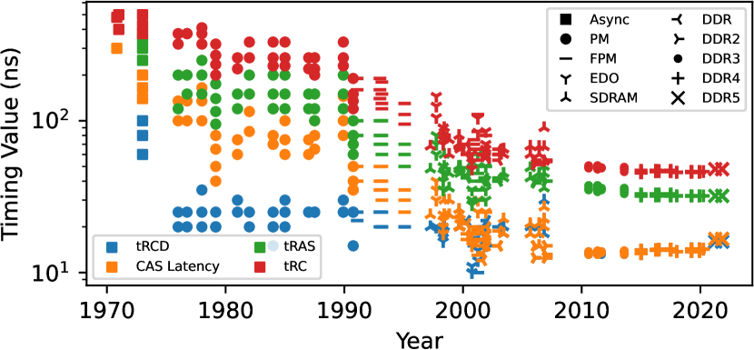
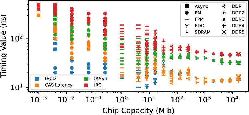
We make three qualitative observations. First, while all four DRAM timing values have roughly decreased over time, improvements have been relatively stagnant for the last two decades (note the logarithmic Y-axis). The bulk of the improvement in timing parameter values occurred during the period of asynchronous DRAM, and following the introduction of SDRAM and DDRn DRAM chips, little to no improvements have been made despite, or possibly as a result of, continual increases in overall chip storage density. Second, CAS latency and tRCD converged to roughly the same values following the introduction of synchronous DRAM. We hypothesize that this is because similar factors affect the latency of these operations, including a long command and data communication latency between the external DRAM bus and the internal storage array [3]. Third, the DDR5 data points appear to worsen relative to previous DDRn points. However, we believe this might be because DDR5 chips are new at the time of writing this article and have not yet been fully optimized (e.g., through die revisions and other process improvements).
To quantify the changes in access timings, we aggregate the data points from Figure 3 by three different categories: time, DRAM standard, and chip capacity. Figure 4, shows the minimum, median, and maximum of the timing parameter values (in log scale) for each 5-year period (top) and DRAM standard (bottom). The data shows that the median tRCD/CAS Latency/tRAS/tRC reduced by 2.66/3.11/2.89/2.89% per year on average between 1970 and 2000 but only 0.81/0.97/1.33/1.53% between 2000 and 2015141414We omit the 2020 data point because 2020 shows a regression in CAS latency due to first-generation DDR5 chips, which we believe is not representative because of its immature technology. for an overall decrease of 1.83/2.10/1.99/2.00% between 1970 and 2015.
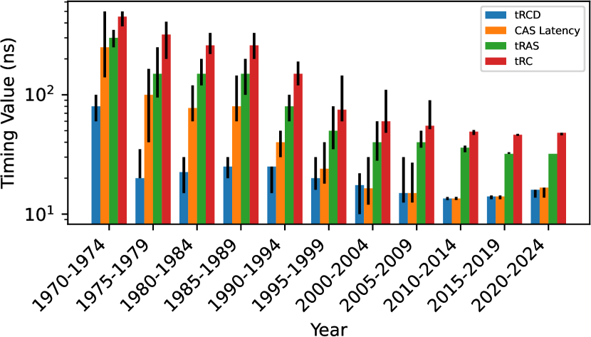
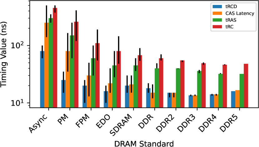
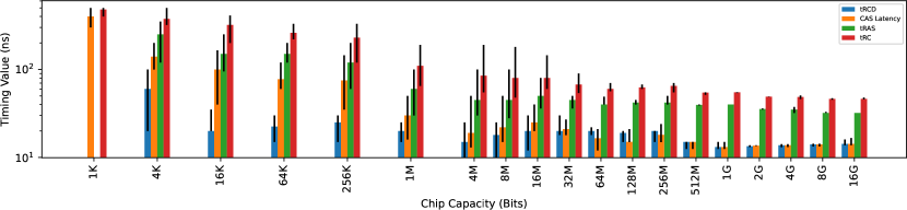
Figure 5 shows the minimum, median, and maximum of the timing parameter values (in log scale) grouped by DRAM chip storage capacity.151515We omit tRCD and tRAS for the 1 Kib chips because they do not use a row address strobe (RAS) signal. We find that the timings follow similar trends as in Figure 4 because higher-capacity DRAM chips are typically introduced more recently and follow newer DRAM standards.
A.2 Current Consumption Trends
We review the evolution of the following key DRAM current consumption measurements, which are standardized by JEDEC and are provided by manufacturers in their datasheets.
-
•
IDD0: current consumption with continuous row activation and precharge commands issued to only one bank.
-
•
IDD4R: current consumption when issuing back-to-back read operations to all banks.
-
•
IDD5B: current consumption when issuing continuous burst refresh operations.
Figure 6 shows how key DRAM current consumption values (in log scale) have evolved across DRAM chips of different years (top) and capacities (bottom). We use different markers to show data points from chips of different DRAM standards. We qualitatively observe that current consumption increased exponentially up until approximately the year 2000, which is about the time at which improvements in access timings slowed down (as seen in Figure 3). After this point, different current consumption measurements diverged as IDD0 values decreased while IDD4R and IDD5B stabilized or increased. We explain this behavior by a change in the way DRAM chips were refreshed as DRAM capacities continued to increase. Earlier DRAM chips refreshed rows using individual row accesses (e.g., RAS-only refresh), which result in comparable behavior for access and refresh operations. In contrast, newer DRAM chips aggressively refresh multiple rows per refresh operation (e.g., burst refresh), which differentiates refresh operations from normal row accesses [186, 363, 364].
We quantify the current consumption values by aggregating the data points from Figure 6 by time and DRAM standard. Figure 7 shows the minimum, median, and maximum values (in log scale) across each 5-year period (top) and DRAM standard (bottom). The data shows that the median IDD0/IDD4R/IDD5B increased by 12.22/20.91/26.97% per year on average between 1970 and 2000 but decreased by 4.62/1.00/0.13% between 2000 and 2015161616Similar to Section A.1, we omit the 2020 data point because the first-generation DDR5 chips exhibit outlying data values (e.g., no data reported for IDD5B in the datasheets). for an overall increase of 0.96/11.5/17.5% between 1970 and 2015.
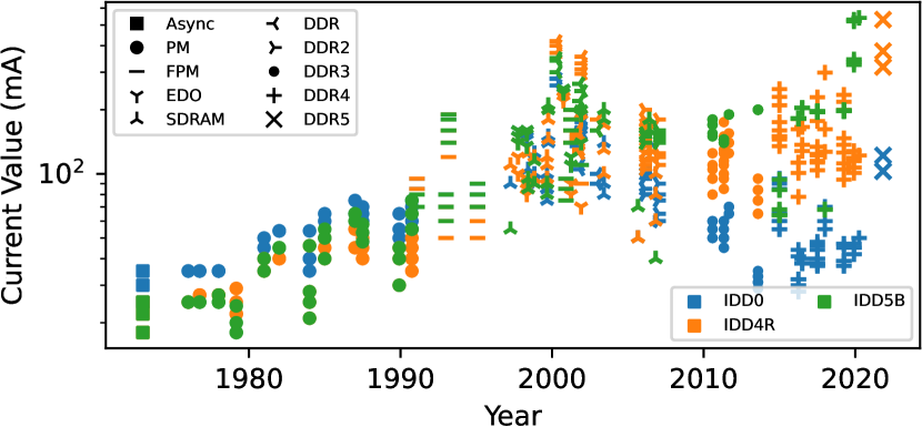
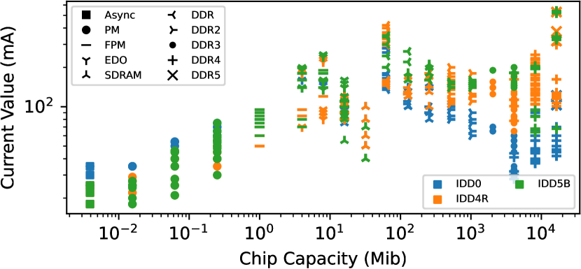
A.3 Relationship Between Timings and Currents
Finally, we examine the high-level relationship between the timing parameter and current consumption values. We find that the two are generally inversely related, which follows from the general principle that faster DRAM chips (i.e., lower timing parameters) require more power (i.e., increased current consumption values). Figure 8 illustrates this relationship for the four timing parameters studied in Section A.1 relative to IDD4R (i.e., the current consumption of read operations).
A.4 DRAM Refresh Timing Trends
DRAM refresh is governed by two key timing parameters:
-
•
tREFI (refresh interval): time between consecutive refresh commands sent by the memory controller.
-
•
tRFC: duration of a single refresh command.
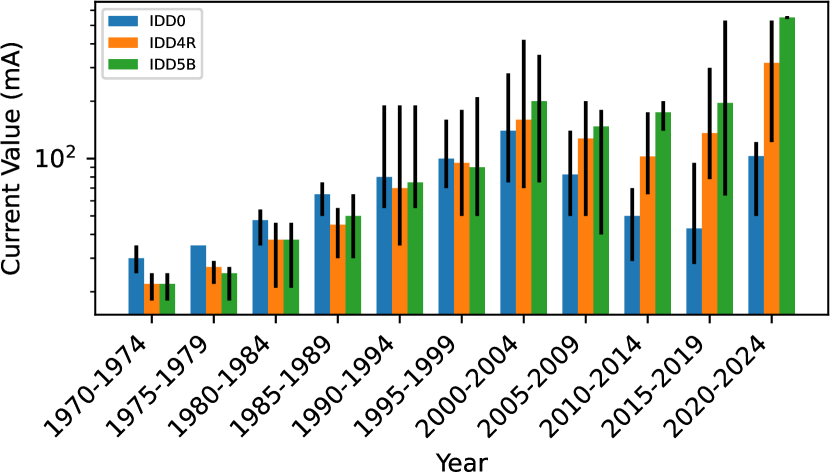
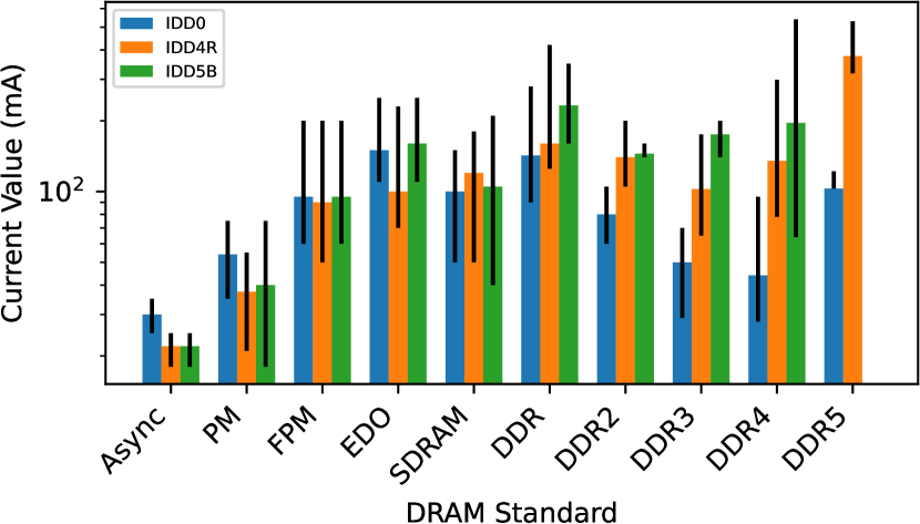
Figure 9 shows how tREFI (left y-axis) and tRFC (right y-axis) evolved across the DRAM chips in our study. We group chips by storage capacity because DRAM refresh timings are closely related to capacity: higher-capacity chips using the same technology require more time or more refresh operations to fully refresh. The error bars show the minimum and maximum values observed across all chips for any given chip capacity.
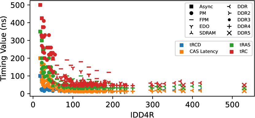
We make three observations. First, tREFI is shorter for higher-capacity DRAM chips (e.g., 62.5 s for an asynchronous 1 Kib chip versus 3.9 s for a 16 Gib DDR5 chip). This is consistent with the fact that higher-capacity chips require more frequent refreshing. Second, tRFC first decreases with chip capacity (e.g., 900 ns for an asynchronous 1 Kib chip versus 54 ns for a 32 Mib SDRAM chip) but then increases (e.g., to 350 ns for a 16 Gib DDR4 chip). This is because rapid improvements in row access times (and therefore refresh timings) initially outpaced the increase in storage capacity. However, starting around 512 Mib chip sizes, row access times improved much more slowly (as observed in Section A.1) while storage capacity continued to increase. Third, the variation in tRFC across chips of each capacity (illustrated using the error bars) decreased for higher-capacity chips. This is because higher-capacity chips follow more recent DRAM standards (i.e., DDRn), which standardize DRAM auto refresh timings. In contrast, older DRAM chips were simply refreshed as quickly as their rows could be accessed (e.g., every tRC using RAS-only refresh).
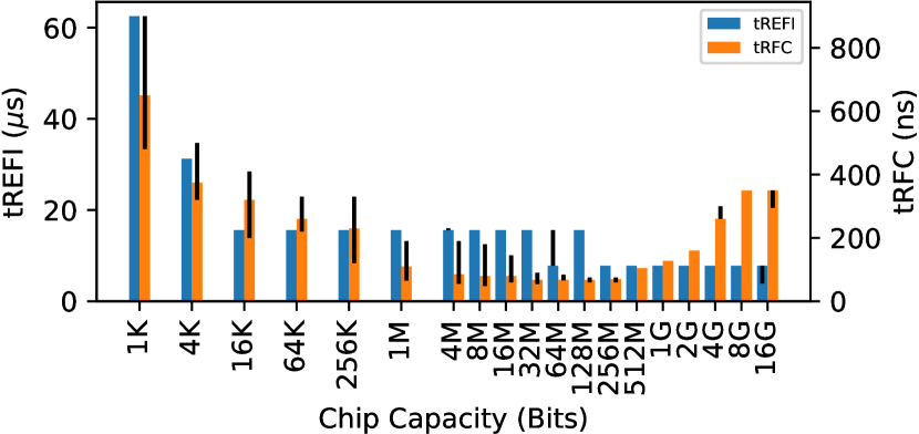
Figure 10 shows the refresh penalty [364, 363], which is defined as the ratio between tRFC and tREFI, for DRAM chips of different storage capacities. The refresh penalty represents the average time that a DRAM rank (or bank) is unavailable for access due to refresh operations [364, 185, 363, 365, 188]. We observe that the refresh penalty exhibits a similar trend to tRFC: the refresh penalty worsens from a median of 1.04% for 1 Kib chips to 2.05% for 16 Kib chips, then improves to 0.43% for 128 Mib chips, and finally worsens to a median of 4.48% (worst-case of 7.56% for DDR5 chips) for 16 Gib chips.
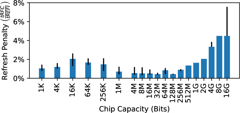
This non-monotonic trend is due to the relative improvements in DRAM access times and storage capacities: DRAM capacities consistently improved while DRAM access times did so only for older, lower-capacity chips (e.g., Mib chips). This is consistent with trends observed in prior work [43, 77, 181, 187, 183, 82], which expect that future, higher-capacity DRAM chips will spend an even larger proportion of time refreshing unless the DRAM refresh algorithm and techniques can be improved.
Appendix B Survey Data Sources
Table 5 itemizes the 58 DRAM datasheets used for our survey in Appendix A. For each datasheet, we show the DRAM chip manufacturer, model number, DRAM standard, year, and capacity. Our full dataset is available online [35].
| Year | Manufacturer | Model Number | Datasheet Source | DRAM Standard | Capacity per Chip (Kib) |
|---|---|---|---|---|---|
| 1970 | Intel | 1103 | \citeSds_intel19701103 | Asynchronous | 1 |
| 1971 | Mostek | MK4006 | \citeSds_mostek1971mk4006 | Asynchronous | 1 |
| 1973 | Mostek | MK4096 | \citeSds_mostek1973mk4096 | Asynchronous | 4 |
| 1976 | Mostek | MK4027 | \citeSds_mostek1976mk4027 | PM | 4 |
| 1976 | Mostek | MK4116P | \citeSds_mostek1976mk4116p | PM | 16 |
| 1978 | Fairchild | F4116 | \citeSds_fairchild1978f4116 | PM | 16 |
| 1979 | Intel | 2118 | \citeSds_intel19792118 | PM | 16 |
| 1981 | Mitsubishi | M5K4164ANP | \citeSds_mitsubishi1981m5k4164anp | PM | 64 |
| 1982 | Mostek | MK4564 | \citeSds_mostek1982mk4564 | PM | 64 |
| 1984 | NTE | NTE4164 | \citeSds_nte1984nte4164 | PM | 64 |
| 1984 | Texas Instruments | TMS4416 | \citeSds_texas1984tms4416 | PM | 64 |
| 1985 | Mitsubishi | M5M4256P | \citeSds_mitsubishi1985m5m4256p | PM | 256 |
| 1987 | Samsung | KM41464A | \citeSds_samsung1987km41464a | PM | 256 |
| 1987 | Texas Instruments | TMS4464 | \citeSds_texas1987tms4464 | PM | 256 |
| 1989 | Texas Instruments | SMJ4464 | \citeSds_texas1989smj4464 | PM | 256 |
| 1990 | Intel | 21256 | \citeSds_intel199021256 | PM | 256 |
| 1991 | Mitsubishi | M5M44100 | \citeSds_mitsubishi1991m5m44100 | FPM | 4096 |
| 1993 | Mitsubishi | M5M44256B | \citeSds_mitsubishi1993m5m44256b | FPM | 1024 |
| 1993 | Mosel Vitelic | V404J8 | \citeSds_mosel1993v404j8 | FPM | 8192 |
| 1995 | Siemens | HYB511000BJ | \citeSds_siemens1995hyb511000bj | FPM | 1024 |
| 1997 | Hyundai | HY5118164B | \citeSds_hyundai1997hy5118164b | EDO | 16384 |
| 1997 | Samsung | KM48S2020CT | \citeSds_samsung1997km48s2020ct | SDRAM | 16384 |
| 1998 | Micron | MT48LC4M4A1 | \citeSds_micron1998mt48lc4m4a1 | SDRAM | 16384 |
| 1998 | Mosel Vitelic | V53C808H | \citeSds_mosel1998v53c808h | EDO | 8192 |
| 1998 | Siemens | HYB39S16400 | \citeSds_siemens1998hyb39s16400 | SDRAM | 16384 |
| 1999 | Samsung | K4S160822D | \citeSds_samsung1999k4s160822d | SDRAM | 16384 |
| 1999 | Samsung | K4S561632A | \citeSds_samsung1999k4s561632a | SDRAM | 262144 |
| 2000 | Amic | A416316B | \citeSds_amic2000a416316b | FPM | 1024 |
| 2000 | ISSI | IS41LV32256 | \citeSds_issi2000is41lv32256 | EDO | 8192 |
| 2000 | Samsung | K4D623237A5 | \citeSds_samsung2000k4d623237a5 | DDR | 65536 |
| 2001 | Alliance | AS4C256K16E0 | \citeSds_alliance2001as4c256k16e0 | EDO | 4096 |
| 2001 | Alliance | AS4C4M4FOQ | \citeSds_alliance2001as4c4m4foq | FPM | 16384 |
| 2001 | ISSI | IS41C4400X | \citeSds_issi2001is41c4400x | EDO | 16384 |
| 2001 | Micron | MT46V2M32 | \citeSds_micron2001mt46v2m32 | DDR | 65536 |
| 2001 | Micron | MT46V32M4 | \citeSds_micron2001mt46v32m4 | DDR | 131072 |
| 2001 | Mosel Vitelic | V58C265164S | \citeSds_mosel2001v58c265164s | DDR | 65536 |
| 2001 | TM Tech | T224160B | \citeSds_tm2001t224160b | FPM | 4096 |
| 2003 | Micron | MT46V64M4 | \citeSds_micron2003mt46v64m4 | DDR | 262144 |
| 2003 | Samsung | K4S560432E | \citeSds_samsung2003k4s560432e | SDRAM | 262144 |
| 2005 | Amic | A43L0632 | \citeSds_amic2005a43l0632 | SDRAM | 32768 |
| 2006 | Elite | M52S32321A | \citeSds_elite2006m52s32321a | SDRAM | 32768 |
| 2006 | ISSI | IS42S81600B | \citeSds_issi2006is42s81600b | SDRAM | 131072 |
| 2006 | Sasmung | K4T51043QC | \citeSds_sasmung2006k4t51043qc | DDR2 | 524288 |
| 2007 | Micron | MT47H256M4 | \citeSds_micron2007mt47h256m4 | DDR2 | 1048576 |
| 2010 | Samsung | K4B4G0446A | \citeSds_samsung2010k4b4g0446a | DDR3 | 4194304 |
| 2011 | Hynix | H5TQ4G43MFR | \citeSds_hynix2011h5tq4g43mfr | DDR3 | 4194304 |
| 2011 | Nanya | NT5CB512M | \citeSds_nanya2011nt5cb512m | DDR3 | 2097152 |
| 2013 | Samsung | K4B4G0446A | \citeSds_samsung2013k4b4g0446a | DDR3 | 4194304 |
| 2015 | Micron | MT40A2G | \citeSds_micron2015mt40a2g | DDR4 | 8388608 |
| 2016 | Hynix | H5AN4G4NAFR | \citeSds_hynix2016h5an4g4nafr | DDR4 | 4194304 |
| 2016 | Samsung | K4A8G165WC | \citeSds_samsung2016k4a8g165wc | DDR4 | 8388608 |
| 2017 | Hynix | H5AN8G4NAFR | \citeSds_hynix2017h5an8g4nafr | DDR4 | 8388608 |
| 2018 | Micron | MT40A | \citeSds_micron2018mt40a | DDR4 | 16777216 |
| 2019 | Hynix | H5AN8G4NCJR | \citeSds_hynix2019h5an8g4ncjr | DDR4 | 8388608 |
| 2019 | Samsung | K4AAG045WA | \citeSds_samsung2019k4aag045wa | DDR4 | 16777216 |
| 2020 | Samsung | K4AAG085WA | \citeSds_samsung2020k4aag085wa | DDR4 | 16777216 |
| 2021 | Hynix | HMCG66MEB | \citeSds_hynix2021hmcg66meb | DDR5 | 16777216 |
| 2021 | Micron | MT60B1G16 | \citeSds_micron2021mt60b1g16 | DDR5 | 16777216 |
IEEEtran \bibliographySreferences