Tunable fractional quantum Hall point contacts in graphene via local anodic oxidation of graphite gates
Abstract
In an all-van der Waals heterostructure, the active layer, gate dielectrics, and gate electrodes are all assembled from two-dimensional crystals. Owing to the absence of dangling bonds within their two-dimensional bulk, these devices host ultraclean electron systems. Here, we describe methods for implementing nanoscale electrostatic control without contaminating critical interfaces. Using a resist-free local anodic oxidation process, we pattern sub-100 nm features in graphite gates which are then integrated into the heterostructure. Using a quantum point contact as a benchmark device, we demonstrate selective partitioning of both integer and fractional quantum Hall edge modes at high magnetic fields. Furthermore, we find evidence for fragile interaction-driven edge reconstruction effects, including the formation of a quantum dot at an electrostatic potential saddle point. Our results pave the way for precision nanoscale experiments on correlated states in these materials, including single anyon control in the fractional quantum Hall regime.
Van der Waals heterostructures have recently emerged as a platform to study the physics of correlated electronic states at both high and zero magnetic fielddean_fractional_2020 ; yankowitz_van_2019 ; balents_superconductivity_2020 ; andrei_marvels_2021 . A central feature is electrostatic tunability, enabling a variety of correlation-driven ground states to be accessed by field effect gating in a single device. Electrostatic control on the nanoscale then allows one- and zero-dimensional structures to be created within a correlated two-dimensional state, opening the door to experiments that probe the structure of interfaces between distinct phases as well as manipulation of single quasiparticles. Local electrostatic control is of particular interest at high magnetic fields, where clean graphene systems host a range of topologically ordered statesdean_fractional_2020 . Manipulating topological edge modes via electrostatic potentials, for example at a quantum point contact or within an edge state interferometer, can reveal information about the quasiparticle charge and statistics nayak_non-abelian_2008 . However, engineering such setups experimentally is limited by the disorder of the edge potential which reduces coherence over mesoscopic distances.
A key driver of continued improvement in sample quality has been the removal of charged impurities, first with the use of high purity two-dimensional crystals of hexagonal boron nitride (hBN) as a substratedean_boron_2010 and encapsulantmayorov_direct_2011 ; wang_one-dimensional_2013 for the graphene layer and more recently the use of graphite, rather than amorphous metal, for the gate layerszibrov_tunable_2017 . These ‘all-van der Waals heterostructures’ take advantage of the fact that their components do not host dangling bonds in their two-dimensional bulk as well as the property that graphene/hBN interfaces appear to be self-cleaninghaigh_cross-sectional_2012 , irreversibly expelling hydrocarbon residues during processing and leaving a pristine interface. Devices fabricated in this manner exhibit rich cascades of fractional quantum Hall states including a host of states not previously observed in III-V semiconductor quantum wells in double layer systemsliu_interlayer_2019 ; li_pairing_2019 ; dean_fractional_2020 , as well as even denominator states in bilayer graphene whose elementary charged excitations are predicted to obey non-Abelian statistics and may provide a promising platform for topologically protected quantum information processing nayak_non-abelian_2008 ; papic_topological_2014 ; zibrov_tunable_2017 ; li_even_2017 ; bonderson_individually_nodate . Developing platforms which leverage these quasiparticles for quantum computing, however, requires electrostatic control on sub-100nm length scales which also varies smoothly over energy scales comparable to the gap of the state in bilayer graphene: V zibrov_tunable_2017 ; li_even_2017 . Moreover, the utility of low-disorder, nanoscale electrostatic potentials is not restricted to the quantum Hall regime. As but one example, recent proposals for manufacturing topological superconductivity in twisted bilayer graphene nanowires require a clean gate-defined interface between superconductivity and two inter-valley coherent states thomson_gate-defined_2021 .
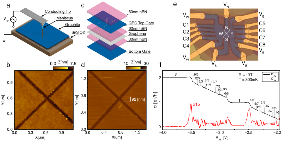
The key features of all-van der Waals heterostructures that enable high mobility are in direct tension with controlling nanoscale electronic potentials. In general, there are two options empowered by traditional electron beam lithography, which is capable of patterning at the required length scales. First, the all-van der Waals geometry may be abandoned, patterning at least some gates from evaporated metal. Alternatively, heterostructures may be assembled and then graphite gates patterned by subtractive processes. Both approaches lead to disorder in critical regions of the device and degraded performance. For example, edge state interferometers remain restricted to the integer quantum Hall regime despite the presence of well formed fractional quantum Hall phases in the two-dimensional sample bulk ronen_aharonov-bohm_2021 ; zimmermann_tunable_2017 ; deprez_tunable_2021 .
Traditional lithographic techniques must consequently be abandoned. In this work we present a process for patterning graphite gates at sub-100 nm length scales using a resist-free process which takes advantage of atomic force microscope-actuated local anodic oxidation (AFM-LAO) of graphite li_electrode-free_2018 . We then integrate these patterned gates directly into van der Waals heterostructures using a low-strain variation on the commonly used dry-transfer process wang_one-dimensional_2013 ; novoselov_2d_2016 ; masubuchi_fabrication_2009 . We qualify our technique using a monolayer graphene quantum point contact (QPC) device operating in the quantum Hall regime. The key figure of merit is the roughness of the confining potential defining the QPC. We quantify this with a series of experiments sensitive to roughness on increasingly small energy scales, starting from the partitioning of integer and then fractional quantum Hall edge modes and culminating in the observation of edge state reconstruction effects. The most sensitive of these effects is the spontaneous formation of an interaction driven quantum dot, which leads to Coulomb blockade peaks corresponding to single quantum levels with energy spacings as low as V.
I Device Fabrication and Geometry
A QPC is formed when a narrow constriction in a two-dimensional device restricts the number of quantized channels through which electrons can flow. In the quantum Hall regime, when the constriction is on the order of the magnetic length , the transmission of chiral edge modes through the QPC varies sensitively with the width. The typical approach to create a QPC in III-V semiconductor quantum wells is to use electron beam lithography techniques to evaporate metal split-gates, separated by 1m or less, and dope the 2DEG under the split gates into the intrinsic band-gap, forming a narrow constriction between the depleted regionsvan_wees_quantized_1988 . This approach is precluded in monolayer graphene by the absence of a band gap; however, at finite magnetic field, Coulomb interactions generate a gap at charge neutrality allowing electrostatic definition of QPCs in the quantum Hall regime by interfacing quantum Hall states with regions of filling factor .
Due to the high quality of all-van der Waals heterostructures zibrov_even-denominator_2018 ; li_even_2017 ; dean_fractional_2020 , it is desirable to create QPCs where all regions bordering the junction are dual-graphite gated. To accomplish this, we first use an atomic force microscope (AFM) to locally oxidizemasubuchi_fabrication_2009 ; li_electrode-free_2018 a cross-shaped geometry into a graphite flake (see Fig. 1a). In this process, a conductive AFM tip is brought close to a graphite surface in a humid environment. Capillary forces form a nano-scale water meniscus butt_using_2006 connecting the tip and graphite surface. When a high frequency excitation is applied to the tip, the voltage drop across the water meniscus catalyzes oxidation of the graphite into gaseous byproducts. Scanning the tip across the graphite surface while this reaction occurs allows nano-scale subtractive lithographyli_electrode-free_2018 in an entirely resist-free process.
Using this technique, 60-70 nm line-widths can be achieved (Fig. 1b). The patterned graphite gate can then be integrated into a heterostructure (Fig. 1c) and deposited on the final substrate (see Methods). Etch byproducts are visible in the as-cut graphite. However, imaging the etched graphite after it is adhered to an hBN flake during the assembly process shows that this residue is not transferred (Fig. 1d). An optical micrograph of a device following additional standard lithographic processing (see Methods) is shown in Fig. 1e; the final device features four isolated gates we denote North (N), South (S), East (E) and West (W) which control transport through the QPC. Notably, prepatterning the graphite means the areas closest to the QPC are not exposed to any fabrication residues, in contrast to graphite gates patterned by plasma-etchingronen_aharonov-bohm_2021 . The high sample quality resulting from this procedure is visible in Fig. 1f, which shows four-terminal longitudinal and Hall conductance measured in the W quadrant.
II Quantum point contacts in the quantum Hall regime
To characterize the operation of our QPC we measure the four-terminal ‘diagonal conductance,’ , which in the integer quantum Hall (IQH) regime gives a direct measure of the number of edge modes transmitted across the device such that datta_electronic_1995 ; zimmermann_tunable_2017 . We use transport contacts in pairs to decrease the contact resistance and improve edge-state equilibration, exciting an AC voltage on contacts C3/C4, and the measuring the current on contacts C5/C6. The diagonal voltage drop, , is measured between C1/C2 and C7/C8. We then define .
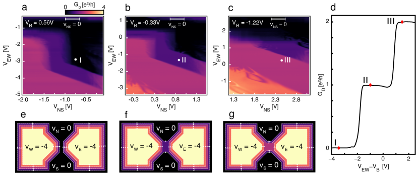
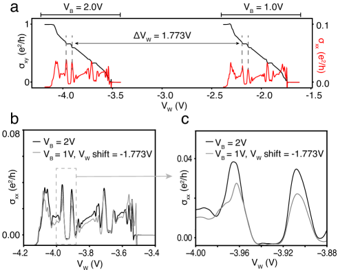
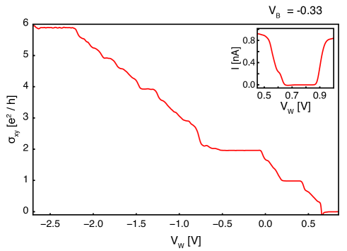
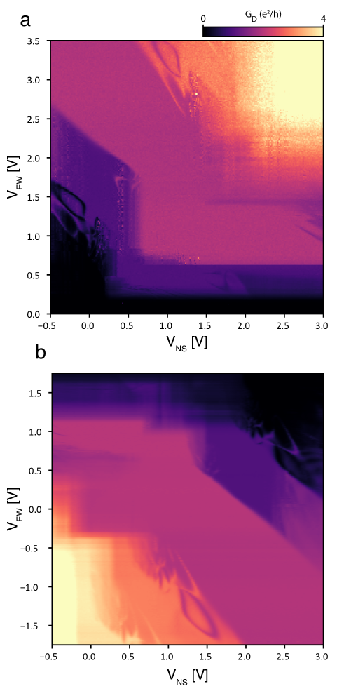
Fig. 2a shows a map of the at B=6 T and T=300 mK as we vary the and . As expected for IQH transport, the conductance maps in Fig. 2a-c are dominated by regions of fixed conductance at integer multiples of , corresponding to transmission of an integer number of chiral edge states across the device. For each conductance map in Fig. 2a-c, the graphite bottom gate, , is fixed to a different voltage. Using the capacitive lever arm (see Fig. 7), the ranges of and are chosen such that the electronic density in each region of the monolayer is kept in the same range in all three panels. The precise mapping of gate voltages to is determined by measuring the Hall effect in the W quadrant (see Fig. 8).
Tracing the behavior of the transitions between conductance plateaus reveals two distinct regimes. In the first, plateau transitions are controlled by only or , producing steps in along either horizontal or vertical lines in the plane. In this regime, the diagonal conductance is primarily determined by the number of edge states transmitted along the physical edge of the device, far from the QPC. For example at point I in Fig. 2a, the filling factor of the north and south regions, , is fixed to , while the E/W regions are fixed to . Point I sits to the right of a vertical transition, solely controlled by , where goes from 0 to 1. Decreasing starting at point I changes the filling from 0 to -1, adding an edge mode in the N/S regions at the physical device boundary and increasing .
In the second regime, the plateau transitions are influenced by both and , producing a step in along lines of slope in the plane. This behavior is expected when edge modes are transmitted through the center of the QPC, where they are equally sensitive to the fringe electric fields of each of the N/S/E/W gates. Consider again point I which sits just above a diagonal transition, where goes from 0 to 1. Near the transition, and no conduction can occur along the etched boundary – all current must be carried via edge modes through the QPC. However, at the transition, may change sharply by either an equal perturbation in or while maintaining . The existence of such transitions in implies the filling factor in the QPC center can be held fixed via equal and opposite modulations of and : lines separating differing values of which are parallel to demarcate sharp boundaries between regions of different filling factor in the center of the QPC itself.
The diagonal steps in shift as a function of (Figs. 2b-c), in contrast to the horizontal and vertical transitions in whose locations are unaffected. This behavior follows from the device electrostatics: Near the device boundary, transport is determined directly by the bulk filling factor in the N/S/E/W regions. Since the graphite bottom gate uniformly modulates the density of the whole monolayer, the role of is merely to induce a chemical potential shift in the whole device which is compensated by offsetting the applied gate voltages. This is not true in the central region, however, which is doped by the fringe fields of N/S/E/W gates.
It follows that tuning the bottom gate while keeping the densities in the N, S, E, and W constant changes the electrostatics of the QPC. Points I-III in Figs. 2a-c correspond to identical carrier densities away from the QPC, with and . At point I, all the edge modes are pinched off and . As is decreased, the filling factor in the QPC changes, leading to the transmission of one additional edge modes at point II and and two additional modes at point III. Fig. 2d shows the continuous evolution between points I, II, and III as a function of , corresponding to tuning the QPC electrostatics. A schematic depiction of the corresponding filling factor maps in real space are shown in Figs. 2e-g, with additional discussion provided in the supplementary information.
To explore QPC operation in the fractional quantum Hall (FQH) regime, edge state transmission must be controlled while maintaining at a fixed, fractional filling. To ensure the absence of edge states in the N/S regions, the N/S gates must also be adjusted to maintain for a given bottom gate voltage. Fortunately, the gap has a finite width in gate voltage due to the large quantum capacitance, allowing us to modulate the shape of the QPC potential using the N/S gates while maintaining .
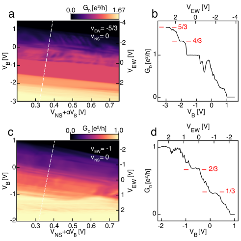
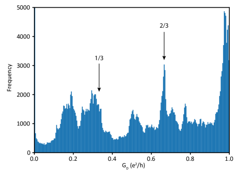
Figs. 3a-b show maps of , measured for at B=13T and T=300mK. We observe two distinct fractionally-quantized plateaus at and above the integer plateau at . The existence of two fractional conductance steps in the state implies that the edge hosts two modes with conductance , and is not expected from conventional models of the edge structure for a sharp confinement potentialjohnson_composite_1991 ; kane_randomness_1994 . However, since the QPC is entirely gate-defined, the moderate slope of the confinement potential allows for reconstruction of the edge states under the influence of Coulomb interactions. Edge reconstruction is controlled by the ratio of the “confinement energy”, (here is taken to be potential perpendicular to a confining edge), and the Coulomb energy . Theoreticallychamon_sharp_1994 , an edge phase transition occurs between the sharp-edge regime () and the soft-edge regime at (). In the soft-edge regime, interactions favor the formation of a non-monotonic density at the boundary, introducing an additional edge mode for the hole-conjugate Laughlin states at meir_composite_1994 as confirmed by experiments in GaAssabo_edge_2017 . For our device operating in the regime corresponding to Fig. 3, we estimate mV/nm, giving meV. This is comparable to the Coulomb energy, meV at B=13T, suggesting that reconstruction effects are energetically allowed.
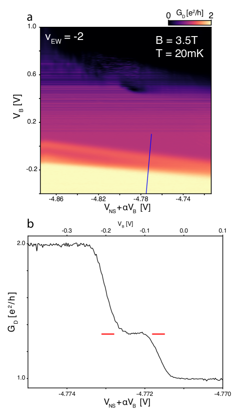
Unexpectedly, the map taken at also shows the emergence of intermediate plateaus between and (Fig. 3c). The clearest of these occur at and , highlighted in 3d. This effect can be observed at fields as low as 3.5T (see Fig. 12). The presence of fractional conductance plateaus within an IQH state is further evidence that edge reconstruction is relevant. Indeed, recent theoretical workkhanna_fractional_2021 has argued that reconstruction can introduce FQH modes even at the edge of an IQH bulk by favoring the spontaneous formation of a side-strip of FQH fluid. This is supported by a recent Mach-Zehnder edge-state interferometry experiment in GaAs bhattacharyya_melting_2019 , where an intermediate 1/3 plateau was observed in the QPC transmission of a bulk state. In contrast to this experiment, we also find a plateau at 2/3, suggestive of the formation of an additional incompressible strip of filling at the gate-defined edge.
III Spontaneous Localization from Edge Reconstruction
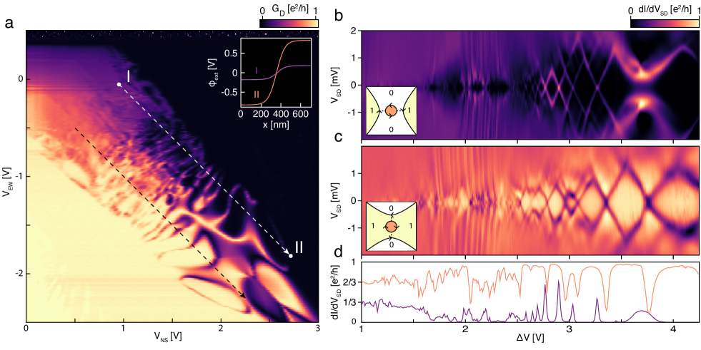
Further evidence for Coulomb-induced reconstruction of the electronic density within the QPC is evident in Fig. 4a, which shows measured over a large range of and at B=13T. The plot is centered around the transition between and , and shows a rich texture of conductance peaks and dips emerging from fractional intermediate plateaus at and in the upper left corner of the plot. Similar features which exhibit identical structure to each other are observed on other conductance steps (see Fig. 9). Figs. 4b and c show the two terminal differential conductance across the quantum point contact, , plotted as a function of the source-drain voltage with the potential difference tuned to follow the contours indicated by dashed white and black arrows, respectively, in Fig. 4a.
Along the white contour in Fig. 4a the junction is nearly pinched off, with conductance dropping to zero between the peaks. Nonlinear conductance in this regime shows diamond-shaped structure typical of transport across a Coulomb blockaded quantum dot, with charging energies as large as 1 meV. This is consistent with a scenario where resonant transmission through the dot allows charge transport between two otherwise fully-reflected edge states in the E and W regions, as illustrated schematically in the inset to Fig. 4b.
Along the black contour in Fig. 4a, nonlinear conductance shows an almost identically-shaped diamond structure, this time with the on-resonance condition corresponding to a decrease in conductance (Fig. 4c). This is again consistent with a a Coulomb blockaded quantum dot in the QPC, but one whose primary effect on transport is to allow backscattering between two otherwise fully-transmitted edge states (see Fig. 4c, inset).
The existence of a quantum dot is not naïvely expected in a quantum point contact where the unscreened electrostatic potential is described by a saddle point. A natural possibility is that a stray disorder potential localizes charge near the nominal saddle point. This hypothesis can be rejected for several reasons. First, nearly identical resonant structure is observed when the sign of all applied gate voltages is reversed (see Fig. 10 and Fig. S2). This rules out local disorder in the QPC of a fixed sign, as such disorder would induce a confining potential in one case but not the other.
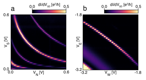
In addition, we can use the four-quadrant gate geometry to determine both the position of the localized charge and its polarizability within the 2D plane. Fig. 5a shows a representative Coulomb blockade peak as function of and , while keeping all other gates constant. The Coulomb peaks will follow the condition , where and are the capacitances to the N and S gates, respectively. The ratio of these capacitances may be inferred from the slope of the Coulomb peak trajectory in the plane, . When , , implying that the dot is equidistant from the two gates. The curvature of the peak trajectory, meanwhile, reveals how the capacitances are changed by the motion of the dot. Evaluating at , we have . The curvature is observed to be positive, and hence . Since is inversely proportional to the distance between the gate and dot, this implies that a positive bias on repels the dot from the gate. This behavior is consistent with a dot trapped at an electrostatic minimum in the N/S direction.
Analogous measurements as a function of and are shown in Fig. 5b. Again, for , , indicating the dot is equidistant from the E and W gates. However, the curvature of the peak trajectories in Fig. 5b are opposite in sign from those in Fig. 5a. This behavior is consistent with a particle trapped in an electrostatic maximum along the E/W direction.
Taken together, these measurements show that the quantum dot is centered at an electrostatic saddle point (see Fig. S2 for analogous data near a simple conductance step). This is puzzling, however, as the presence of intrinsic Coulomb blockade would seem to require a stable extremum of the potential, and a saddle point potential does not support any long-lived localized states, even in a magnetic field hegde_quasinormal_2019 ; floser_transmission_2010 .
The observed localization can be accounted for by considering the same Coulomb-induced edge reconstruction responsible for fractional plateaus in Fig. 3d. Generally, edge state reconstruction may lead to non-monotonic density profiles along a smooth potential step chamon_sharp_1994 ; khanna_fractional_2021 . Along the translation-invariant electrostatic edge between two quantum Hall phases, the resulting electronic density retains the spatial symmetry of the underlying potential, resulting in formation of a series of strips at the boundary between the two phases. In a more complex geometry such as the QPC potential studied here, the same mechanism can favor the formation of more complicated structures that still maintain the 180∘-rotation symmetry of the underlying potential, such as an isolated dot of nonzero density at the center of the QPC.
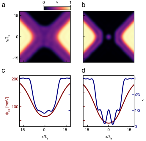
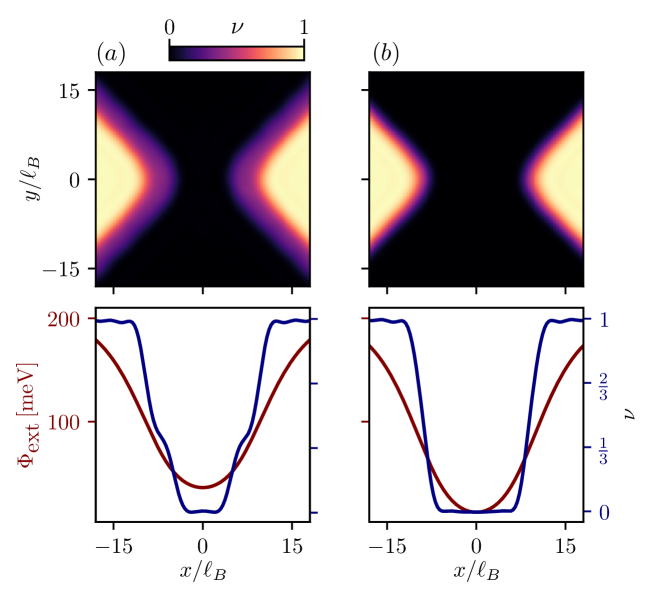
To evaluate the plausibility of a reconstruction-induced quantum dot we use a self-consistent Thomas-Fermi model to calculate the reconstructed density within the QPC. Our calculations account for the nontrivial density dependence of the chemical potential yang_experimental_2021 within a partially-filled LL, as well as the realistic device geometry (see methods and supplementary information for a detailed description of the numerical simulations). Fig. 6a-b shows the calculated density for and . For the softest potential, in panel a, an intermediate side-strip of fractional filling is observed at each boundary between and . As increases, reconstruction becomes less favorable, and an isolated island of filling factor spontaneously forms in the center of the junction. Crucially, this island is isolated from the surrounding regions of non-zero density by depletion regions, which may form tunnel barriers between the dot and the reservoirs on either side.
Both regimes of reconstruction correspond directly to observations in Fig. 4. At point I along the dashed white line, where and the applied potential is thus the softest, we observe fractionally-quantized conductance, , corresponding to transmission of a single fractional edge mode, in agreement with Fig. 6a. As is increased, (starting half-way between I and II where ) Coulomb peaks appear corresponding to the existence of a quantum dot as in Fig. 6b. Our simulations suggest that the quantum dot is composed of an island at fractional filling, raising the possibility that few or single fractionally charged quasiparticles in this platform can be readily localized even with a geometry which, in the absence of Coulomb interactions, forbids trapping single particles. Additionally, in light of our simulations the highly symmetric nature of the resonant reflected features observed in Fig. 4a may likely be interpreted as the particle-hole conjugate to the scenario presented in Fig. 6. While our experiment at present cannot test these hypotheses, future experiments, for example measuring the shot noise across the QPC, may give direct evidence for the trapping of fractional quasiparticles in the dot.
IV Conclusions
We have shown that AFM-based local oxidation lithography of graphite gates allows for nanoscale potential control in ultra-clean two-dimensional devices. By realizing clean quantum point contacts in the fractional quantum Hall regime, our measurements pave the way for the full complement of characterizations of ground state topological order. For example, in semiconductor quantum wells QPCs are the essential component for measurements of the Luttinger liquid parameter radu_quasi-particle_2008 , quantized thermal Hall effectsbanerjee_observation_2018 ; banerjee_observed_2017 , and anyon interferometrynakamura_direct_2020 . Our observation of a spontaneous Coulomb blockade also suggests that creating single-quasiparticle quantum dots that may serve as the building block for a topological quantum bitbonderson_individually_nodate , may be readily achievable. More generally, the techniques we describe will enable a new generation of devices across a variety of ultra-clean all-van der Waals heterostructures incorporating high-complexity integrated graphite gates.
V Methods
V.1 van der Waals Heterostructure Assembly
Graphene and hBN were mechanically exfoliated from bulk crystals using a combination of thermal release tape and scotch magic tape. The initial mother-tape is prepared using 3M Scotch-brand magic tape for graphite or 3M Scotch-brand greener magic tape for hBN. For hBN, thermal release tape is adhered to the mother-tape to generate a daughter tape. For graphite, the daughter-tape is made with 3M Scotch-brand magic tape. The daughter-tape is removed from the mother-tape, cleaving the bulk crystals along the c-axis, then transferred onto a 1cm x 1cm doped Si chip with 285nm of thermally-grown SiO2 on the surface. For graphite, the substrate is heated to C for 60 seconds, before removing the tape quickly to reduce glue residue remaining on the SiO2 surface. For hBN, the daughter-tape is transferred onto the SiO2 surface at room temperature and is removed from the SiO2 slowly. The Si/SiO2 substrates are cleaned by a standard solvent process: the chip is cleaned in acetone for 5 minutes in a high power ultrasonic bath, followed by an IPA wash, and finished with an N2 blow-dry. Additionally, for graphite the SiO2 surface is treated in O2 plasma at 100W and 300mTorr for 60 seconds in order to promote adhesion of large multilayers. The resulting exfoliated crystals are then characterized by optical microscopy.
AFM-LAO was performed on a Bruker Dimension Icon AFM. Exfoliated graphite flakes, prepared as described above, are loaded into the AFM. The humidity is controlled using a bang-bang style humidity controller. The plant is formed by a beaker filled with 250mL of deionized water placed on a hot plate at C. Once the humidity sensor measures higher than 50% RH, the hot-plate is switched off. We pattern sub 100 nm crosses into a 3 nm graphite flake to form the top gate of the quantum point contact. This is accomplished using a Pt/Ir coated Arrow-NcPt AFM probe from nanoandmore. A topographical map of the graphite flake is obtained and the cross pattern is placed in an area with no visible defects. The lithography is performed in Bruker’s Nanoman software package which allows for precise control of the direction, speed, and deflection of the conducting AFM probe. Graphite can be etched with AFM-LAO under a variety of conditions, however we have found that lithography performed in contact mode with an 18V peak-to-peak excitation at 150kHz provided the smallest line-widths achievable in our system. For new AFM probes, typical line-widths are on the order of 60-70 nm . This leads to a QPC critical dimension (tip-to-tip distance) between 90 and 100 nm . However, due most likely to hydrocarbon build up or natural wear on the AFM probe, the cut-width broadens to 100 nm after 150 m of cutting.
Before assembling the van der Waals heterostructure we fabricate a ‘transfer-slide:’ a PDMS stamp adhered to a glass slide with a polycarbonate laminate transferred on top used to ‘pick-up’ the first layer of hBN. Initially, 8g of Sylgard 184 PDMS is mixed in a 10:1 ratio by weight with a curing agent and poured into a standard 100 mm plastic petri dish. The PDMS is left to cure at room temperature for 24 hours in a vacuum chamber in order to remove any bubbles that formed during mixing. Additionally, another 3g of Sylgard 184 PDMS solution is mixed with a curing agent and left to cure partially at room temperature under vacuum for 2 hours. A PDMS cylinder is cut out using a 2 mm hole punch from the 8g PDMS batch and is then adhered to a glass slide using the partially cured PDMS. An additional droplet of partially cured PDMS is pipetted onto the cylinder in order to form a dome. Slides are left to finish curing for another 24 hours at room temperature. The resulting slides are then inspected under an optical microscope for dirt particulates.
The polycarbonate laminate is made from a 13.3% wt/vol ratio of Bisphenol-A polycarbonate (PC) in cyclopentanone. Unaided, cyclopentanone will only dissolve a 4% wt/vol solution of PC, however by using the QSonica 500 ultrasonic wand, solutions up to 15% wt/vol can be made. This recipe was derived from previous work by Abbas abbas_nanofabrication_2013 . Due to its significantly lower vapor pressure than chloroform, PC dissolved in cyclopentanone can be effectively spun onto a Si substrate. Thin films of PC are prepared by spinning the mixture onto a Si substrate at 1400 rpm for 60 seconds. The thin film is then subsequently transferred onto a domed PDMS stamp. The transfer slide is heated between C to C for 5 minutes in order to increase the adhesion between the PC film and the PDMS stamp as well as to remove any air bubbles that may have formed during transfer of the film.
We begin the assembly of the van der Waals heterostructure by picking up an hBN flake larger than 100um in both width and length. Ensuring the first hBN has the largest area aids in assembling the remaining layers since subsequent crystals will adhere entirely to another van der Waals material. The transfer slide is engaged at a tilt angle, with the substrate heated to C, and with the touch-down point 100-150um away from the center of the first hBN layer. Once the transfer slide is brought into near contact the substrate is heated to C. This causes the transfer slide to fully engage and laminate over the first hBN layer. The substrate is then cooled naturally back down to which retracts the transfer slide and removes the target hBN flake from the SiO2. Next, the AFM-LAO etched graphite top gate is picked up while entirely encapsulated by the large initial hBN layer. There are a number of advantages to using a domed PDMS transfer slide, one of which is that the engage point is in the center of the PDMS stamp, as opposed to the edge, which has fewer dust particulates that can interfere with assembly. Moreover, domed PDMS transfer slides are known to reduce strain during vDH assembly saito_independent_2020 ; it turns out this technique is critical for picking up AFM-LAO nano-structures without inducing tears or folds.
The PC laminate is extremely uniform as a result of being spun onto a Si substrate. This also minimizes a common issue in assembling van der Waals heterostructures where the polycarbonate exhibits stochastic adherence to the SiO2 substrate. This often causes a ‘jerk’ like motion during stacking which easily can cause graphite nano-structures to tear. The remaining layers are assembled in the same manner; the full resulting device stack can be seen in Fig. 1c. The stack is then deposited onto a doped silicon substrate with 285nm of thermally grown oxide, which forms the basis for a global bottom gate used to dope the graphene contacts. This is accomplished by engaging the transfer slide and heating the substrate to C (above the glass transition temperature of PC) to detach the PC from the PDMS stamp. The laminate is then dissolved in chloroform for a minimum of 30 min. Afterwards, the sample is rinsed in acetone and IPA, and then blown-dry with N2.
V.2 Device Post Processing
Heterostructures are post-processed using standard electron beam lithography, vacuum deposition, and dry-etching processes. A device-defining plasma etch is used to separate the nanotextured graphite into four quadrants that we label North (N), South (S), East (E), and West (W): this is accomplished by inductively coupled plasma (ICP) etching in 40 sccm of CHF3 and 4 sccm of O2. This etch also separates the graphene contacts C1-8 such that any two contacts are only connected through the dual-gated region. Additionally, the conducting Si substrate is used to dope each contact and prevent the formation of p-n junctions at the boundary between the contacts and the dual-gated region. Finally, several trenches are etched across the boundary to the dual-gated region to introduce local scattering sites that improve equilibration between the contacts and quantum Hall edge modes in the device region.
The etch mask is patterned by lifting off 40nm of Al using a polymethyl methacrylate (PMMA) A4 495K / A2 950K bilayer resist. The PMMA is exposed using a 30kV electron-beam in an FEI SEM at 375uC/cm2 and developed in a mixture of DI:IPA 1:3 kept at C. Al is deposited at 0.3A/s and the lift off is done for over 12 hours in N-Methyl-2-Pyrrolidone (NMP). Post etching, the Al is dissolved in AZMIF300 photoresist developer which contains % by weight of Tetramethylammonium hydroxide (TMAH). Edge contacts are deposited onto the exposed graphene contacts and graphite gates using the same bilayer PMMA mask. Before vacuum deposition, a brief contact cleaning etch in an ICP with 40 sccm of CHF3 and 9 sccm of O2 is performed. Subsequently, a metal stack of Cr/Pd/Au 3/15/185 nm is deposited and lifted off. Special care is taken to deposit the Cr layer at 0.3A/s in order to improve coating uniformity.
V.3 Measurement
Experiments were performed in a dry dilution refrigerator with a base temperature of 20mK. Electronic filters are used in line with transport and gate contacts in order to lower the effective electron temperature. To improve edge mode equilibration to the contacts most measurements are performed at 300mK unless otherwise noted. Electronic measurements were performed using standard lock-in amplifier techniques. For the diagonal conductance measurements an AC voltage bias at 17.77Hz is applied via a 1000x resistor divider to (see Fig. 1c for contact references) C3-4 and the resulting current is measured using an Ithaco 1211 trans-impedance amplifier on C5-6 with a gain of A/V. The voltage is measured between contacts C1-2 and C7-8 with an SR560 voltage pre-amplifier with a gain of 1000. For two terminal measurements the same AC bias is applied to contacts C1-4 and the current is measured via C5-8. DC bias was added on top of the AC bias using a passive summer.
V.4 Thomas-Fermi calculation
We consider a classical effective model wherein the electron density of the two-dimensional electron gas adjusts according to the local electrostatic potential and compressibility of an interacting Landau-level (LL). The classical energy functional can be decomposed into the Hartree energy, the interaction with an externally applied potential , and the remainder,
| (1) | ||||
contains not only the exchange-correlation energy but also single-particle contributions (e.g. inter-LL interactions, disorder, Zeeman energies, etc.). If varies slowly compared with , we may neglect the dependence of the functional on the gradient and employ the local density approximation (LDA),
| (2) |
where is determined for a system at constant density . Our aim here is to find the density configuration corresponding to the global minimum of the free energy .
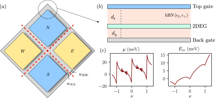
The geometry we consider is shown in Fig. S3a-b. There are four top gates a distance above the sample and one back gate a distance below, between which the space is filled by hBN with dielectric constant and laturia_dielectric_2018 . The N/S gates and the E/W gates are shifted by and , respectively, from the center (see Fig. S3a-b). We make an approximation by treating the cut-out “X”-shaped region to define the gates as a metal held at fixed voltage (rather than as a vacuum). This allows us to analytically solve for the electrostatic Green’s function and gate-induced potentials without resorting to e.g. COMSOL simulations.
For a coarse-grained system with a finite resolution grid, the classical energy functional becomes
| (3) | ||||
where is the grid area, is the total area, and . is set by the gate-screened Coulomb interaction,
| (4) |
and . is the one body potential term arising from the potential on the sample due to the adjacent gates,
| (5) |
where is the top gate potential and is the back gate potential.
The remaining energy is defined by integrating the chemical potential ,
| (6) |
which encodes information about the IQH and FQH gaps and the electron compressibility. For we use the experimentally measured value obtained for monolayer graphene in the FQH regime () we reported in an earlier work, Ref yang_experimental_2021 .
Physically, can only vary on the scale of the magnetic length due to the underlying quantum Hall wavefunction. To capture this feature, we implement a square grid with periodic boundary conditions and meshing much finer than the scale of , and then evaluate with respect to the Gaussian convoluted density profile 111We first use an unbounded range for to determine the external potential that fix bulk filling and . Then we constrain to fall in between and such that any transition from to in has a finite width of scale .
| (7) |
where is the corresponding normalization factor. We use a basin-hopping global optimizer with local L-BFGS-B minimization to vary and find the lowest energy configuration.
Within this framework, we tune the E/W gate potentials such that deep in the bulk and the N/S gate potentials such that . Various effects of reconstruction can then be explored by appropriately tuning the smoothness of the potential at the to interface (e.g. by tuning the channel width , gate distances or gate voltages ).
VI Data Availability
The data that support the findings of this study are available from the corresponding author upon reasonable request.
VII Acknowledgements
The authors thank J. Folk and A. Potts for comments on the manuscript, and C.R. Dean and J. Swan for advice on humidity stabilization. Work at UCSB was primarily supported by the Air Force Office of Scientific Research under award FA9550-20-1-0208 and by the Gordon and Betty Moore Foundation EPIQS program under award GBMF9471. LC and NS received additional support from the Army Research Office under award W911NF20-1-0082. TW and MZ were supported by the Director, Office of Science, Office of Basic Energy Sciences, Materials Sciences and Engineering Division of the U.S. Department of Energy under contract no. DE-AC02-05-CH11231 (van der Waals heterostructures program, KCWF16). KK was supported by the U.S. Department of Energy, Office of Science, National Quantum Information Science Research Centers, Quantum Science Center. CR was supported by the National Science Foundation through Enabling Quantum Leap: Convergent Accelerated Discovery Foundries for Quantum Materials Science, Engineering and Information (Q-AMASE-i) award number DMR-1906325. K.W. and T.T. acknowledge support from JSPS KAKENHI (Grant Numbers 19H05790, 20H00354 and 21H05233).
VIII Author Contributions
L.A.C and A.F.Y conceived of the experiment. L.A.C and N.S. fabricated the device measured. L.A.C and N.S performed the measurements. L.A.C, N.S, M.Z., T.W., K.K., and A.F.Y analyzed the data and wrote the paper. M.Z. and S.V. proposed the simulation methodology. T.W., K.K., and C.R. performed numerical calculations based on the proposed theoretical modeling. T.T. and K.W. synthesized the hexagonal boron nitride crystals.
IX Competing Interests
The authors declare no competing interests.
X Additional Interests
The authors declare no additional interests.
XI References
References
- (1) Dean, C., Kim, P., Li, J. I. A. & Young, A. Fractional Quantum Hall Effects in Graphene. In Fractional Quantum Hall Effects: New Developments, 317–375 (World Scientific, Singapore, 2020).
- (2) Yankowitz, M., Ma, Q., Jarillo-Herrero, P. & LeRoy, B. J. van der Waals heterostructures combining graphene and hexagonal boron nitride. Nature Reviews Physics 1, 112–125 (2019).
- (3) Balents, L., Dean, C. R., Efetov, D. K. & Young, A. F. Superconductivity and strong correlations in moiré flat bands. Nature Physics 16, 725–733 (2020).
- (4) Andrei, E. Y. et al. The marvels of moiré materials. Nature Reviews Materials 1–6 (2021).
- (5) Nayak, C., Simon, S. H., Stern, A., Freedman, M. & Das Sarma, S. Non-Abelian anyons and topological quantum computation. Reviews of Modern Physics 80, 1083–1159 (2008).
- (6) Dean, C. R. et al. Boron nitride substrates for high-quality graphene electronics. Nature Nanotechnology 5, 722–726 (2010).
- (7) Mayorov, A. S. et al. Direct evidence for micron-scale ballistic transport in encapsulated graphene at room temperature. 1103.4510 (2011).
- (8) Wang, L. et al. One-Dimensional Electrical Contact to a Two-Dimensional Material. Science 342, 614–617 (2013).
- (9) Zibrov, A. A. et al. Tunable interacting composite fermion phases in a half-filled bilayer-graphene Landau level. Nature 549, 360–364 (2017).
- (10) Haigh, S. J. et al. Cross-sectional imaging of individual layers and buried interfaces of graphene-based heterostructures and superlattices. Nat Mater 11, 764–767 (2012).
- (11) Liu, X. et al. Interlayer fractional quantum Hall effect in a coupled graphene double layer. Nature Physics 15, 893–897 (2019).
- (12) Li, J. I. A. et al. Pairing states of composite fermions in double-layer graphene. Nature Physics 15, 898–903 (2019).
- (13) Papic, Z. & Abanin, D. A. Topological Phases in the Zeroth Landau Level of Bilayer Graphene. Physical Review Letters 112, 046602 (2014).
- (14) Li, J. I. A. et al. Even denominator fractional quantum Hall states in bilayer graphene. Science eaao2521 (2017).
- (15) Bonderson, P., Nayak, C., Reilly, D., Young, A. F. & Zaletel, M. Individually tunable quantum dots in all-van der Waals heterostructures.
- (16) Thomson, A., Sorensen, I., Nadj-Perge, S. & Alicea, J. Gate-defined wires in twisted bilayer graphene: from electrical detection of inter-valley coherence to internally engineered Majorana modes. arXiv:2105.02891 [cond-mat] (2021).
- (17) Ronen, Y. et al. Aharonov-Bohm effect in graphene-based Fabry-Pérot quantum Hall interferometers. Nature Nanotechnology 16, 563–569 (2021).
- (18) Zimmermann, K. et al. Tunable transmission of quantum Hall edge channels with full degeneracy lifting in split-gated graphene devices. Nature Communications 8, 14983 (2017).
- (19) Déprez, C. et al. A tunable Fabry-Pérot quantum Hall interferometer in graphene. Nature Nanotechnology 16, 555–562 (2021).
- (20) Li, H. et al. Electrode-Free Anodic Oxidation Nanolithography of Low-Dimensional Materials. Nano Letters 18, 8011–8015 (2018).
- (21) Novoselov, K. S., Mishchenko, A., Carvalho, A. & Neto, A. H. C. 2D materials and van der Waals heterostructures. Science 353, aac9439 (2016).
- (22) Masubuchi, S., Ono, M., Yoshida, K., Hirakawa, K. & Machida, T. Fabrication of graphene nanoribbon by local anodic oxidation lithography using atomic force microscope. Applied Physics Letters 94 (2009).
- (23) van Wees, B. J. et al. Quantized conductance of point contacts in a two-dimensional electron gas. Phys. Rev. Lett. 60, 848–850 (1988).
- (24) Zibrov, A. A. et al. Even-denominator fractional quantum Hall states at an isospin transition in monolayer graphene. Nature Physics 14, 930–935 (2018).
- (25) Butt, H.-J., Farshchi-Tabrizi, M. & Kappl, M. Using capillary forces to determine the geometry of nanocontacts. Journal of Applied Physics 100, 024312 (2006).
- (26) Datta, S. Electronic Transport in Mesoscopic Systems. Cambridge Studies in Semiconductor Physics and Microelectronic Engineering (Cambridge University Press, Cambridge, 1995). URL https://www.cambridge.org/core/books/electronic-transport-in-mesoscopic-systems/1E55DEF5978AA7B843FF70337C220D8B.
- (27) Johnson, M. D. & MacDonald, A. H. Composite edges in the =2/3 fractional quantum Hall effect. Physical Review Letters 67, 2060–2063 (1991).
- (28) Kane, C. L., Fisher, M. P. A. & Polchinski, J. Randomness at the edge: Theory of quantum Hall transport at filling =2/3. Phys. Rev. Lett. 72, 4129–4132 (1994).
- (29) Chamon, C. d. C. & Wen, X. G. Sharp and smooth boundaries of quantum Hall liquids. Physical Review B 49, 8227–8241 (1994).
- (30) Meir, Y. Composite edge states in the = 2/3 fractional quantum Hall regime. Physical Review Letters 72, 2624–2627 (1994).
- (31) Sabo, R. et al. Edge reconstruction in fractional quantum Hall states. Nature Physics 13, 491–496 (2017).
- (32) Khanna, U., Goldstein, M. & Gefen, Y. Fractional edge reconstruction in integer quantum Hall phases. Physical Review B 103, L121302 (2021).
- (33) Bhattacharyya, R., Banerjee, M., Heiblum, M., Mahalu, D. & Umansky, V. Melting of Interference in the Fractional Quantum Hall Effect: Appearance of Neutral Modes. Physical Review Letters 122, 246801 (2019).
- (34) Hegde, S. S., Subramanyan, V., Bradlyn, B. & Vishveshwara, S. Quasinormal Modes and the Hawking-Unruh Effect in Quantum Hall Systems: Lessons from Black Hole Phenomena. Physical Review Letters 123, 156802 (2019).
- (35) Flöser, M., Champel, T. & Florens, S. Transmission coefficient through a saddle-point electrostatic potential for graphene in the quantum Hall regime. Physical Review B 82, 161408 (2010).
- (36) Yang, F. et al. Experimental Determination of the Energy per Particle in Partially Filled Landau Levels. Physical Review Letters 126, 156802 (2021).
- (37) Radu, I. P. et al. Quasi-Particle Properties from Tunneling in the =5/2 Fractional Quantum Hall State. Science 320, 899–902 (2008).
- (38) Banerjee, M. et al. Observation of half-integer thermal Hall conductance. Nature 559, 205–210 (2018).
- (39) Banerjee, M. et al. Observed quantization of anyonic heat flow. Nature 545, 75–79 (2017).
- (40) Nakamura, J., Liang, S., Gardner, G. C. & Manfra, M. J. Direct observation of anyonic braiding statistics. Nature Physics 16, 931–936 (2020).
- (41) Abbas, A. Nanofabrication Using Electron Beam Lithography: Novel Resist and Applications. Master of Applied Science, University of Waterloo, Waterloo, Ontario CA (2013).
- (42) Saito, Y., Ge, J., Watanabe, K., Taniguchi, T. & Young, A. F. Independent superconductors and correlated insulators in twisted bilayer graphene. Nature Physics 1–5 (2020).
- (43) Akash Laturia, Maarten L. Van de Put & William G. Vandenberghe. Dielectric properties of hexagonal boron nitride and transition metal dichalcogenides: from monolayer to bulk. npj 2D Mater Appl 2 (2018).
- (44) We first use an unbounded range for to determine the external potential that fix bulk filling and . Then we constrain to fall in between and such that any transition from to in has a finite width of scale .
- (45) In the experiment yang_experimental_2021 , was obtained at , which introduces a difference in energy scale of by a factor of 1.19 relative to at which we carry out our calculations.
- (46) It is advantageous to take a smaller here than the experimental so that the necessary system size , and hence the number of variational parameters in the optimization, remains tractable.
- (47) Milliken, F., Umbach, C. & Webb, R. Indications of a luttinger liquid in the fractional quantum hall regime. Solid State Communications 97, 309–313 (1996).
- (48) Ando, M., Endo, A., Katsumoto, S. & Iye, Y. Conduction through point contacts in fractional quantum hall liquid. Physica B: Condensed Matter 249-251, 426–429 (1998).
- (49) Baer, S. et al. Interplay of fractional quantum hall states and localization in quantum point contacts. Phys. Rev. B 89, 085424 (2014).
XII Extended Data Figures
Supplementary Information: Tunable fractional quantum Hall point contacts in graphene via local anodic oxidation of graphite gates
XIII Extended Integer QPC Operation
| Index | ||||
|---|---|---|---|---|
| I | 1 | -4 | 0 | -1 |
| II | 1 | -2 | -1 | -1 |
| III | 1 | -1 | -2 | 0 |
| IV | 1 | -1 | -2 | -1 |
| V | 2 | -2 | -2 | -2 |
| VI | 0.7 | -1 | -4 | -2 |
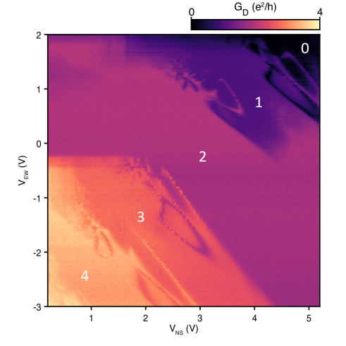
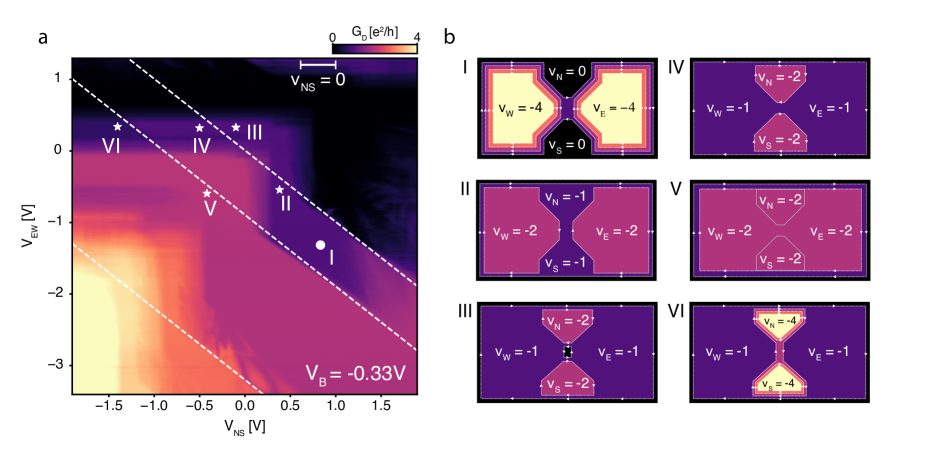
The full parameter space that determines the value of when tuned with and has features which depend on either or individually or features perpendicular to (indicated as dashed white lines in Fig. S1a). The former are dominated by physics at the etched edge of the device where the edge modes of a junction are fully equilibrated zimmermann_tunable_2017 . The latter are interpreted as boundaries between operating points that have differing values of – the filling factor in the center of the device, determined by the fringe fields of the four quadrant top gates (for a fixed ). Fig. S1a has several points denoted by roman numerals which correspond either to QPC operation or conductance through the edge of the device. Fig. S1b shows an illustration of the inferred filling factor in each region of the device for each point marked in Fig. S1a. This information, along with the associated for each point is repeated in the table.
Point VI is of particular note since it falls to the left of a boundary in , where is a fractional value below 1, that is intersected by a dashed line. This indicates the transition is sensitive to the potential at the QPC, but is in a region where at least one edge mode is transmitted along the edge of the device since . The corresponding filling factors at VI are , , and . Starting from point IV, where , as becomes more negative, the filling factor in the QPC is more strongly doped towards . Eventually, at point VI, the filling factor in the QPC increases to , and an edge mode bridges the north and south regions through the bulk. This creates a scattering channel across the device that reduces the conductance to the expected value of for a junction of the given filling factors (-1, -2, -1) zimmermann_tunable_2017 ; deprez_tunable_2021 . This shows it is possible to see QPC behavior even with a background conductance through the etched edge of the device, however the value of requires some interpretation. Consequently, for most experiments presented in the main text we focus exclusively on regimes where there is no conduction along the edge of the device, simplifying possible interpretations of fractional values of .
XIV Extended Information on Interaction-Driven Quantum Dots
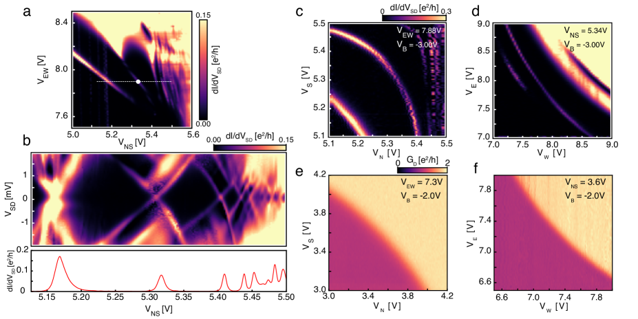
The Coulomb blockaded resonant structure is fairly ubiquitous in this device. Fig. S2 presents a series of several resonances which exhibit Coulomb blockade on the electron side of the device at 9T and 20mK. Fig. S2a shows the resonances in the (, ) plane, where and . The chemical potential of the quantum dot is modulated directly with the N/S gates as is swept along the dashed white line in Fig. S2a. Fig. S2b shows the differential conductance as a function of and along this trajectory along with the zero-bias cut.
The sharp peaks in Fig. S2b have some finite curvature in the (, ) plane. Since the slope here is a direct measure of , where is the total capacitance of the dot, this indicates that as is increased, the capacitance of the N/S gates to the dot is decreasing relative to . This is consistent with the dot being squeezed in the N/S direction as is increased. This can be further corroborated by the observation that as is increased in Fig. S2a, the slope of successive resonances decreases, indicating a decreased sensitivity to modulations in – i.e., as increases. Additionally, Fig. S2c-d shows a representative resonance as as function of vs. as well as vs. . Much like the analysis in the main text (Fig. 5), when or , the slope in the / plane or the (, ) plane is near , indicating the dot is roughly centered in the QPC.
The behavior of a monotonic transition in as a function of vs. and vs. can be seen in Fig. S2e-f. It has been well established that monotonic steps in conductance at a quantum Hall QPC can be described by the scattering of electrons in a magnetic field at a saddle point potential floser_transmission_2010 . Qualitatively, the behavior of the monotonic transmission step, and the Coulomb blockaded resonances in S2c-d are similar; the monotonic transmission step and the resonance both have the same curvature in the (, ) or (, ) plane. This further verifies the conclusion that the quantum dots are sitting on top of an externally applied potential which forms a saddle point, not a 2D well.
XV Thomas-Fermi calculation of the local density in the QPC
XV.1 Fractional Reconstruction
To approximate the experimental device, we simulate a system with magnetic field (magnetic length ) 222In the experiment yang_experimental_2021 , was obtained at , which introduces a difference in energy scale of by a factor of 1.19 relative to at which we carry out our calculations, gate distances and channel widths on a system with gridsize 333It is advantageous to take a smaller here than the experimental so that the necessary system size , and hence the number of variational parameters in the optimization, remains tractable..
For a finite system and mesh size, we find that edge reconstruction is most easily observed when is increased by a factor of (for the data shown here, is increased by 1.8x). One possible origin of this discrepancy is screening from the filled LLs. In Ref. yang_experimental_2021 it was found the screening from virtual inter-LL transitions (which is implicitly included in our , since we use experimental data) reduces the IQH gaps, and hence features in , by about a factor of 1.4 relative to their unscreened values. However, our phenomenological model does not account for inter-LL screening in the electrostatic contributions and . Decreasing their scale relative to can thus be interpreted as a very crude implementation of LL-screening in the remaining energy functionals. Of course other approximations are in play as well, e.g. the local density approximation, so at the outset we do not expect more than phenomenological agreement with experiment.
At a translationally invariant boundary between to , previous variational calculations have suggested edge-state reconstruction makes it energetically favorable to form an additional strip of khanna_fractional_2021 . However, in a QPC geometry where translation symmetry is broken, the effects of reconstruction are much richer and consequently require numerical treatment to fully characterize. In Fig. 6 of the main text, we demonstrate the effects of edge-reconstruction in a QPC as a function of the potential smoothness quantified by the ratio . To accomplish this, we fix and tune the smoothness of the confining potential via the relative magnitudes of and . For the smallest value of , we find in Fig. 6a reconstructed strips which extend far enough into the QPC that they merge, corresponding to a fractional conductance across the QPC (, ). With increasing , in Fig. 6b the strips become narrower and an island of fractional filling is formed in the center of the QPC (, ). As shown in Fig. S4a, we confirmed upon further increasing (, ), the strips become even narrower and the island disappears. For extremely sharp edges (, ), in Fig. S4b the strips disappear entirely leaving the expected density profile for a edge everywhere in the QPC.
We note that the strips are smoothly connected to the bulk (i.e. not separated by a region of ) even for very smooth confining potentials, which is consistent with variational calculations which more accurately account for the energetics of to edges beyond the local-density approximation khanna_fractional_2021 . For a line cut taken directly across the to interface (e.g. between the east and north gates), the confining potential gives a confinement energy and for the two scenarios in Fig. 6a-b respectively, and for the scenario where the island of fractional filling disappears (Fig. S4a). The gate potentials reported here are slightly smaller than actual values used in the experiment. In the experiment, the bulk filling far from the QPC can be as high as even though the local filling at the QPC will give to interfaces as we simulate here (see Fig. 4 of the main text). Since we simulate only the small region close to the QPC, the effective gate voltages we employ will necessarily reflect a smaller range than that of the experiment.
In generic quantum Hall systems, it is widely believed that disorder and localized impurities are responsible for the formation of localized states in the QPC which facilitate resonant tunneling and are responsible for the non-monotinicity observed in conductance measurements across QPC transmission steps Milliken1996 ; Ando1998 ; Baer2014 . In the device studied in this paper, we do not expect such disorder, and the localized states were attributed to an entirely intrinsic mechanism based purely on including the Coulomb interaction at the soft gate-defined edges of the QPC. That picture is supported by our Thomas-Fermi calculations, where we have shown explicitly that the Coulomb interaction itself is sufficient to favor reconstruction of a local island. We see then that by appropriate tuning of the gate voltages, one can reproduce a Coulomb blockade and fractional transmission in close approximation to the experimental findings of this report.
XV.2 Integer Reconstruction
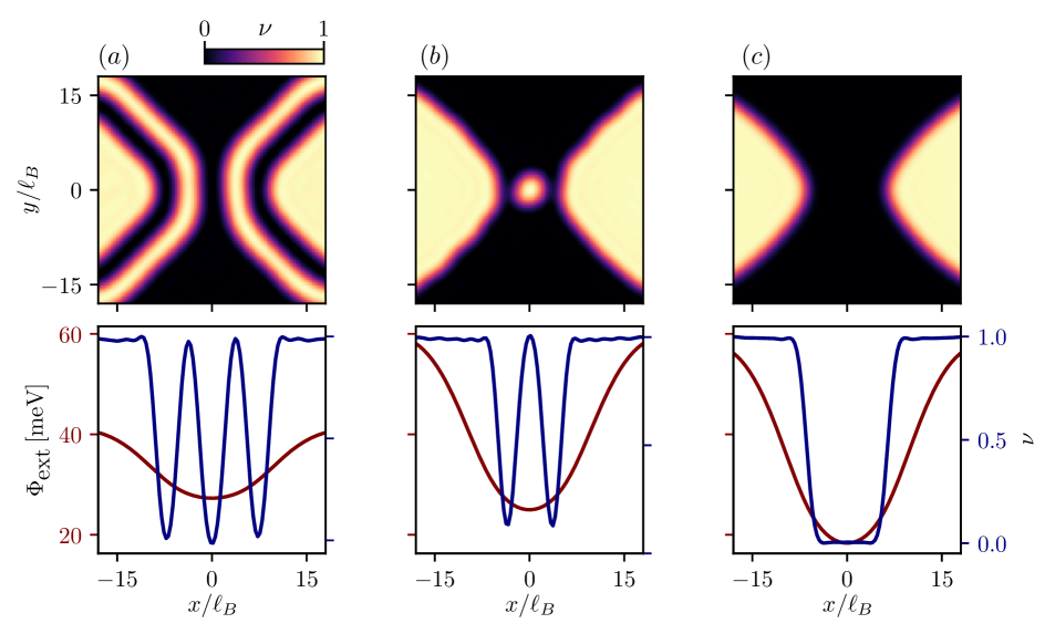
Now we turn our attention to the possibility of reconstructed strips and islands with integer filling. Integer reconstruction can be made more energetically favorable in the numerics by reducing the magnitude of such that redistributing integer charge along the edge out competes the energy gained from from forming a correlated FQH strip. Fixing , and as before, we now take , and work on a system grid which is large.
In Fig. S5, we demonstrate edge-reconstruction as a function of the confining potential smoothness tuned via the gate voltages. For the smallest value of , we find in Fig. S5a reconstructed strips that exist throughout the QPC, (, , ). With increasing , in Fig. S5b the formation of an island of integer filling within the QPC (, , ) is observed, and in Fig.S5c, for the largest value of , a monotonic transition from to is recovered everywhere in the QPC (, , ).
In contrast to the strips, the reconstructed strips in Fig. S5a are separated from the bulk by fully depleted regions, which is also consistent with variational calculations khanna_fractional_2021 . For a line cut taken directly across the to interface (e.g. between the east and north gates), the confining potential gives a confinement energy and for three scenarios Fig. S5a-c respectively. We leave a more detailed study of the interplay of integer and fractional reconstruction in this QPC geometry to future work.