Purcell enhancement of erbium ions in TiO2 on silicon nanocavities
Abstract
Isolated solid-state atomic defects with telecom optical transitions are ideal quantum photon emitters and spin qubits for applications in long-distance quantum communication networks. Prototypical telecom defects such as erbium suffer from poor photon emission rates, requiring photonic enhancement using resonant optical cavities. Many of the traditional hosts for erbium ions are not amenable to direct incorporation with existing integrated photonics platforms, limiting scalable fabrication of qubit-based devices. Here we present a scalable approach towards CMOS-compatible telecom qubits by using erbium-doped titanium dioxide thin films grown atop silicon-on-insulator substrates. From this heterostructure, we have fabricated one-dimensional photonic crystal cavities demonstrating quality factors in excess of and corresponding Purcell-enhanced optical emission rates of the erbium ensembles in excess of 200. This easily fabricated materials platform represents an important step towards realizing telecom quantum memories in a scalable qubit architecture compatible with mature silicon technologies.
keywords:
Purcell enhancement, rare earth ions, erbium, quantum opticsArgonne National Laboratory] Nanoscience and Technology Division, Argonne National Laboratory, Lemont, IL 60439 \alsoaffiliation[Argonne National Laboratory] Center for Molecular Engineering, Argonne National Laboratory, Lemont, IL 60439 University of Chicago] Pritzker School of Molecular Engineering, University of Chicago, Chicago, IL 60637 \alsoaffiliation[Argonne National Laboratory] Materials Science Division, Argonne National Laboratory, Lemont, IL 60439 \alsoaffiliation[Argonne National Laboratory] Center for Molecular Engineering, Argonne National Laboratory, Lemont, IL 60439 Argonne National Laboratory] Materials Science Division, Argonne National Laboratory, Lemont, IL 60439 \alsoaffiliation[Argonne National Laboratory] Center for Molecular Engineering, Argonne National Laboratory, Lemont, IL 60439 University of Chicago] Pritzker School of Molecular Engineering, University of Chicago, Chicago, IL 60637 \alsoaffiliation[Argonne National Laboratory] Materials Science Division, Argonne National Laboratory, Lemont, IL 60439 Argonne National Laboratory] Materials Science Division, Argonne National Laboratory, Lemont, IL 60439 \alsoaffiliation[University of Chicago] Pritzker School of Molecular Engineering, University of Chicago, Chicago, IL 60637 University of Chicago] Pritzker School of Molecular Engineering, University of Chicago, Chicago, IL 60637 \alsoaffiliation[Argonne National Laboratory] Materials Science Division, Argonne National Laboratory, Lemont, IL 60439 University of Chicago] Pritzker School of Molecular Engineering, University of Chicago, Chicago, IL 60637 \alsoaffiliation[Argonne National Laboratory] Materials Science Division, Argonne National Laboratory, Lemont, IL 60439 Argonne National Laboratory] Nanoscience and Technology Division, Argonne National Laboratory, Lemont, IL 60439 Argonne National Laboratory] Nanoscience and Technology Division, Argonne National Laboratory, Lemont, IL 60439 Argonne National Laboratory] Materials Science Division, Argonne National Laboratory, Lemont, IL 60439 \alsoaffiliation[Argonne National Laboratory] Center for Molecular Engineering, Argonne National Laboratory, Lemont, IL 60439 \alsoaffiliation[University of Chicago] Pritzker School of Molecular Engineering, University of Chicago, Chicago, IL 60637 University of Chicago] Pritzker School of Molecular Engineering, University of Chicago, Chicago, IL 60637 \alsoaffiliation[Argonne National Laboratory] Materials Science Division, Argonne National Laboratory, Lemont, IL 60439 University of Chicago] Pritzker School of Molecular Engineering, University of Chicago, Chicago, IL 60637 \alsoaffiliation[Argonne National Laboratory] Materials Science Division, Argonne National Laboratory, Lemont, IL 60439 \alsoaffiliation[Argonne National Laboratory] Center for Molecular Engineering, Argonne National Laboratory, Lemont, IL 60439
Main Text
Rare earth ion defects in solid-state hosts are key candidate qubits for applications in quantum computing and communication owing to their inherent spin-photon interface and long coherence times. These properties have enabled critical demonstrations of optical quantum memory protocols 1 based on light-matter entanglement2 and entanglement distribution3. Quantum technologies geared toward distribution of quantum information over long distances require qubits that interface with telecom photons to avoid huge propagation losses over optical fiber networks. Because the trivalent ion of erbium (Er3+) has a transition in the telecom C-band, there has been interest in using erbium ions as optically-addressable quantum memories using persistent spectral hole burning techniques 4, 5, 6 and spin-based 7 quantum memories in quantum communication, including at the level of single ions 8, 9, 10. However, significant engineering steps are needed to enhance the low photon emission rates from individual rare earth ions, which tend to have long radiative lifetimes.
One direct way to reduce the radiative lifetime is to use an optical cavity to enhance the emission through the Purcell effect 11. The majority of Purcell enhancement studies on rare earth ions have involved devices derived from rare earth-doped bulk crystals, namely heterogeneous integration with deposited amorphous Si resonators 5 or bonded Si photonics 8, 12, focused ion beam milling of bulk crystals 13, 6, 14, 15, or incorporating relatively small erbium-doped samples into tunable distributed Bragg reflector-based fiber cavities 16, 17. These approaches are all appealing because they leverage the generally good performance of well-studied host materials for Er3+ (Y2SiO5 5, 8, 6, 14, YVO4 18, CaWO4 19, 20). Furthermore, these prior approaches have led to important cutting-edge demonstrations towards single rare-earth ion quantum memories, including single-shot spin state readout 10, 21, 15. However, such approaches may not allow for the on-chip scalability needed for wide deployment of quantum memories in large-scale quantum networks. For instance, estimates for fault-tolerant quantum repeater protocols show that hundreds or thousands of communication qubits are necessary to perform the requisite (operational and loss) error correction for quantum communication over long distances (1000 km) 22. In addition, the implementation of a fully CMOS-compatible process flow can enable easy integration with on-chip filters, phase shifters, and beamsplitters for on-chip photon routing 23. In the vein of technological scalability with Si, there has also been considerable interest on low concentration implantation of erbium ions into Si nanostructures 24. While this approach might have the greatest technological upside for directly unifying Si photonics with erbium-based quantum memories, early work has shown that the size mismatch between Er3+ and the crystalline lattice leads to myriad substitutional and interstitial sites with closely spaced spectral emission25, 26, and further experiments are needed to resolve the the best defects for various applications.
In addition to ease of Si photonic integration—assessed by the ability to grow on Si and perform straightforward fabrication—there are a variety of additional considerations for a candidate material to serve as a high-quality host for Er3+ such as a minimal or controlled level of background nuclear spins, a wide bandgap, the number of substitutional sites available, and site symmetries 27, 28, 29. To that end, previous measurements have suggested that rutile TiO2 would be a good host for erbium because of narrow optical and spin linewidths in implanted bulk crystals owing to the nonpolar symmetry of the substitutional erbium site and the low natural abundance of nuclear spins, respectively 30. Furthermore, TiO2 thin films can be grown on Si using a variety of deposition techniques 31, 32, are CMOS-compatible, and are amenable to standard fluorine- and chlorine-based dry etch chemistries for top-down device fabrication 33. Recent work has shown Er-doped TiO2 thin films grown on Si substrates via molecular beam deposition32. Some salient features from that recent work are that the TiO2 thin films were polycrystalline and the dominant TiO2 phase (rutile or anatase) could be tuned by varying the substrate temperature during growth. Furthermore, the inhomogeneous linewidths for the best buffered devices were as low as 5 GHz, which was substantially narrower than some of the epitaxial thin film control samples grown on better lattice-matched substrates (SrTiO3 or sapphire). Molecular beam deposition is particularly appealing for these types of heterostructures because of the inherent control of the Er3+ doping profile and doping density, in order to spectrally resolve single ions. Furthermore, unintentional Er3+ doping from the TiO2 itself is anticipated to be lower than for the more common yttrium-containing oxides due to relatively high concentrations of trace lanthanides in yttrium precursors.
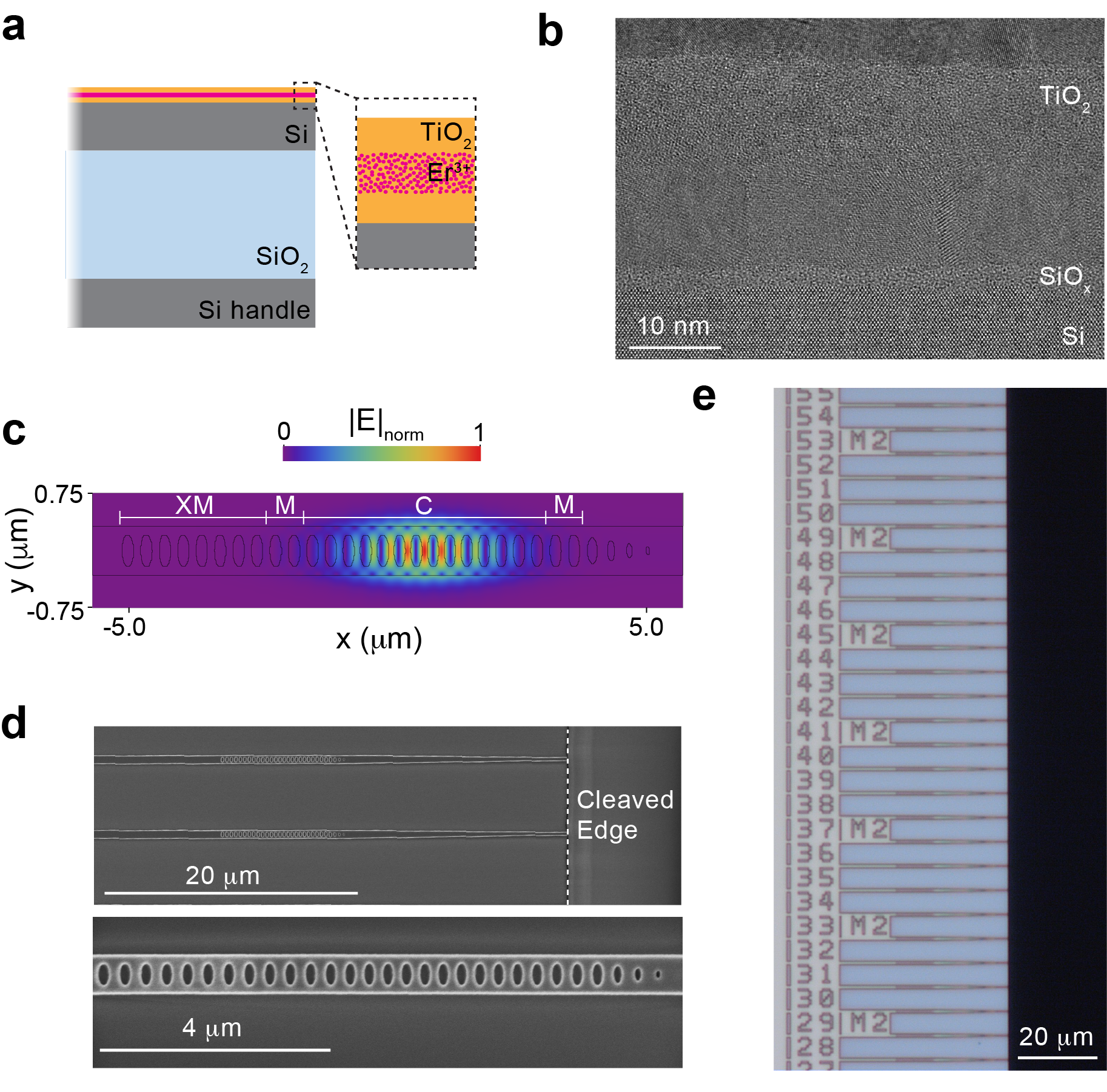
In this Letter, we show early progress on top-down nanofabrication of photonic crystal cavities comprising thin layers of Er-doped TiO2 grown directly atop Si films. The thin films explored are similar to those discussed previously 32, but consist of an Er-doped TiO2 heterostructure grown on commercial silicon-on-insulator (SOI) substrates typically used by the Si photonics community: Si device layer thickness of 220 nm atop a buried oxide (see Methods). Within each TiO2 heterostructure there are three TiO2 layers of equal thickness: an erbium-doped layer sandwiched between undoped top and bottom buffer layers, and each layer is , giving a total film thickness of (Fig. 1a). The estimated Er3+ density within the doped layer is 35 ppm (see Methods). The TiO2 layers for this sample are grown at a substrate temperature of 520 °C. As shown in Fig. 1b, transmission electron microscopy (TEM) cross-sectional imaging reveals that the TiO2 layer is polycrystalline, and there is a thin oxide layer (2 nm) at the Si/TiO2 interface, as was seen previously for lower temperature growth. However, unlike the previous demonstration, the polycrystalline film has both large and small grains visible, and the grains nearest the Si interface are bigger ( nm) than those near the top of the TiO2 layer (1 nm). The cause of this gradient in grain size and effect on eventual Er properties is currently still under investigation. The roughness of the top surface of the TiO2 is approximately 1 nm according to the cross-sectional TEM. Using 3D FDTD simulations, we have designed one-dimensional photonic crystal cavities for our Si/TiO2 heterostructure. Figure 1c shows the computed fundamental (dielectric) mode with a predominant TE-like polarization in the plane of the TiO2 film. The photonic crystal devices consist of a waveguide with identical, elliptically shaped holes and a parabolic reduction of the lattice constant to generate a defect in the photonic bandgap 8 (Fig. 1d, bottom). The photonic crystal cavities are patterned via conventional electron-beam lithography and dry etching through both the TiO2 and Si device layers (see Methods and Supporting Information). After etching and hardmask removal, the waveguide is cleaved along alignment marks under a microscope, beyond the inverse-taper (Fig. 1d, top). We employ an end-fire measurement configuration, where a lensed optical fiber is used to couple light in/out of the device. As a demonstration of the inherent scalability of this scheme, we fabricate hundreds of photonic crystal devices on each chip, a representative cluster of which is shown in Fig. 1e.
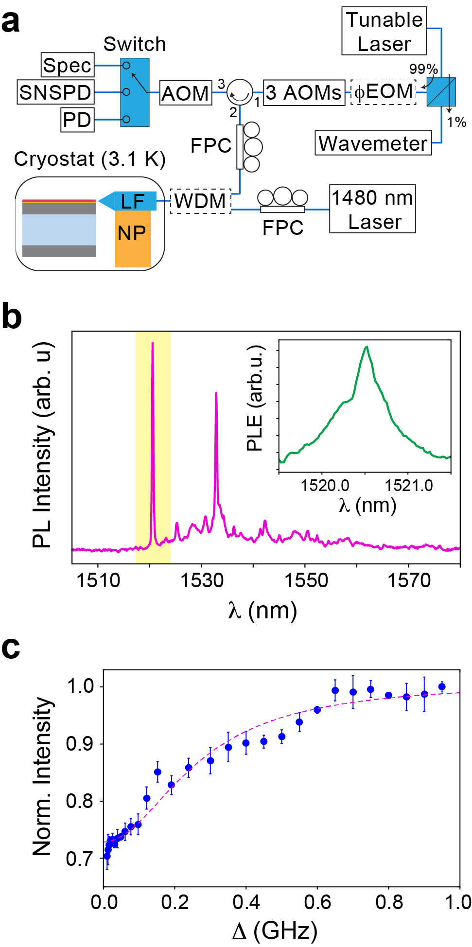
A schematic of our experimental setup used to measure these devices is shown in Fig. 2a. We perform our measurements in a closed-cycle cryostat with a base temperature of . The sample is fixed to the cold finger and the lensed fiber is mounted on a 3-axis nanopositioner to enable addressing of different devices. Using a tunable telecom C-band laser, we primarily probe devices with pulse lengths ranging from 1 to and collection times after the pulse are sufficient to enable decay of the emission (see Methods). The pulses are routed to the sample via a fiber circulator and polarization controller to match the polarization of the cavity mode. We then measure the fluorescence from the sample, back through the lensed fiber and circulator, and directed to either a superconducting nanowire single photon detector (SNSPD), a spectrometer with InGaAs camera, or a photodiode. The one-way coupling efficiency (see Methods) is fairly poor at approximately 15%, but it is sufficient to probe these particular devices because of the relatively large number of ions in the cavity-coupled ensembles. We also have a fiber wavelength division multiplexer (WDM) that can be added into the path of port 2 of the circulator for off-resonant photoluminescence (PL) measurements using a 1480 nm diode laser. Off-resonant PL measurements on a waveguide-only device (no cavity) reveal a variety of peaks from 1520 nm to 1560 nm, as shown in Fig. 2b. The largest peak near 1520.5 nm is attributed to substitutional Er in the rutile phase of TiO2 30, whereas the other dominant peak near 1533 nm is attributed to substitutional Er in anatase 34, as confirmed previously with electron diffraction measurements32. This particular sample is polyphase, which has been seen previously for TiO2 thin films grown at intermediate temperatures 32. The intensity of the substitutional rutile transition—relative to the subsitutional anatase peak—is much stronger in this sample compared to previous thin film results when grown near 520°C32. The origin of this TiO2 phase discrepancy is still under investigation. Similarly, the origin of the minor peaks could be due to a variety of factors, such as different localized phases within the TiO2, Er3+ residing in different substitutional/interstitial sites, or crystal field-split transitions, but additional control samples and experiments are needed.
Resonant photoluminescence excitation (PLE) measurements on the waveguide-only device near 1520.56 nm are performed using a narrowband, tunable CW laser and modulated into pulses with emission from the Er3+ detected during a collection window following each pulse. The lifetime decay curve and associated total PLE intensity at that pump wavelength are integrated after numerous pulses (see Methods). Resonant PLE extracts a linewidth of 0.4 nm (Fig. 2b inset), which is similar to the result from off-resonant pumping. The inhomogeneous linewidth represents the distribution in Er3+ transition energies along the entire device that is over long, and this inhomogeneous linewidth is similar to that measured in predominantly rutile thin film samples using a confocal microscope geometry with a spot size of approximately 32. Given that the inhomogeneous linewidth of the Er3+ in rutile transition is relatively broad, it is important to investigate if the homogeneous linewidth of the emitters is sufficiently narrow to enable cavity-based lifetime enhancement (i.e., the “bad cavity” limit). To that end, we have performed transient spectral hole burning measurements on a waveguide-only device to find an upper bound on the homogeneous linewidth and spectral diffusion 24 for the rutile transition (Fig. 2c). Using the pulsed resonant laser PLE scheme described above, we have employed an additional phase modulator (EOM, Fig. 2a) to generate two sidebands each with a frequency detuning, , from the carrier frequency. We can then measure the relative PLE intensity change as is swept but the laser carrier wavelength is maintained at the rutile transition, 1520.56 nm, and the total pump power is near saturation for the ensemble. If is larger than the spectral diffusion linewidth of the erbium ions, the ions are no longer pumped to saturation and the total fluorescence increases. If we plot the normalized intensity as a function of laser sideband-carrier detuning (Fig. 2c), we can fit a inverted Lorentzian lineshape with a half-width half-maximuum (HWHM) of MHz, which sets the upper bound on the spectral diffusion-limited homogeneous linewidth35. While this homogeneous linewidth is substantially narrower than the inhomogeneous linewidth (Fig. 2b), it is still quite large compared to the natural linewidth of Er3+ in rutile TiO2 (sub kHz). It is possible that further optimization of the top capping layer in these devices can reduce the spectral diffusion of the Er emitters 32.
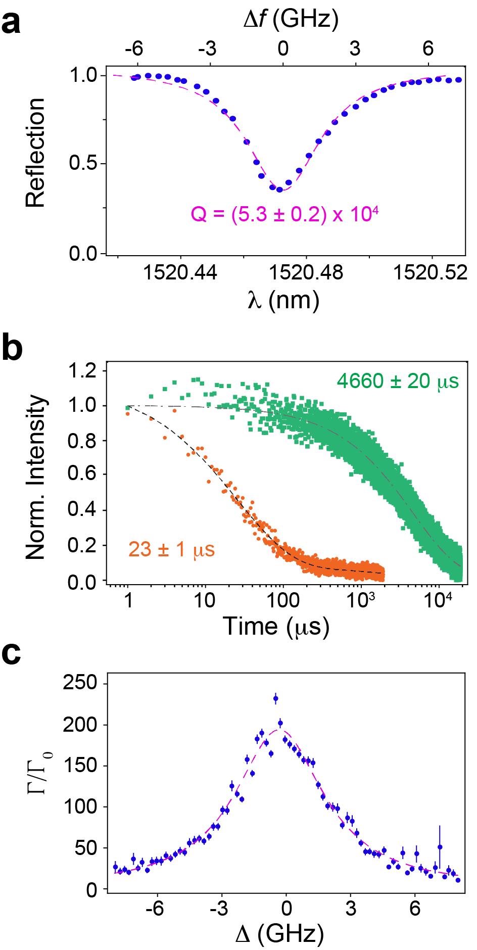
We have the ability to tune the cavity resonance in situ using a combination of controlled gas adsorption and desorption techniques while near base temperature. We use N2 condensation via a gas nozzle directed at the sample to deposit a thin layer of ice on the cavity which increases the refractive index of the mode, resulting in a redshift of its resonance36. We can also deterministically desorb the ice through localized heating, whereby we use relatively strong CW laser excitation tuned directly to the cavity resonance to induce two-photon absorption and heating in the Si, but only at the cavity region, which leads to a blueshift of the cavity resonance (see Methods). Furthermore, this heating is sufficiently localized that cavities in neighboring waveguides—separated by only —can be tuned independently of one another, which can be useful for future two-cavity interference experiments. We can directly measure the spectral position and linewidth of the cavity resonance by detecting the wavelength-dependent reflection of the narrowband laser light using a photodiode. If we perform this measurement close to the rutile transition, we typically see cavity quality factors (Q) near 5. A prototypical cavity reflection scan at is shown in Fig. 3a. Through the use of control devices with and without TiO2 films, the quality factors in general are currently limited by scattering due to the roughness of the top surface of the TiO2 rather than sidewall roughness of the waveguide or cavity holes from the dry etching, though absorption in spectral regions of high Er3+ density also plays a role (see below).
Our resonant pulsed laser measurements reveal the optical lifetime of all ions that couple to the device, which includes ions well-coupled to the cavity, ions poorly coupled to the cavity—whether because of position or polarization—and those that couple only to the bare waveguide. Therefore, we use a stretched exponential function to capture the variety of decay times, where the time constant () in the fit represents the fastest time decay within the ensemble37. Using this technique, the lifetime of the Er ions coupled to a waveguide-only device give a natural lifetime of (Fig. 3b), which is close to the time constant of 5.1 ms measured in implanted/annealed bulk TiO2 at low temperature30. In comparison, the decay time for those ions which couple most strongly to the cavity, when it is tuned onto the rutile transition at 1520.56 nm, show a greatly decreased decay time of . This represents a decay rate enhancement of 200-fold.
We next measure the emission rate enhancement as a function of the detuning between the cavity resonance and the Er3+ rutile transition. To do so, we perform a systematic redshift of the cavity resonance via gas condensation and measurement of the optical lifetime with the resonant laser fixed at the rutile transition. Figure 3c shows the increase in decay rate relative to the natural decay rate as the cavity resonance is tuned across the transition. The cavity-enhanced emission has a Lorentzian linewidth of , which is modestly broader than the cavity linewidth measured via reflection (). However, this can be explained by the increase in absorption when the cavity is resonant with the Er3+ transition versus the reflection scan which is measured at () to the blue of the transition (see Supporting Information). The general agreement of the decay rate enhancement lineshape with that of the cavity suggests that the radiative speedup is due to the cavity rather than non-radiative recombination induced by device fabrication. In addition, the lack of a plateau in Fig. 3c confirms that the system is in the bad cavity limit, i.e. , where is the homogeneous linewidth of the emitters and is the cavity linewidth, in agreement with the transient spectral hole measurement in waveguide-only devices.
In this Letter, we have shown optical addressing of Er3+ ions in rutile phase TiO2 grown on commercial SOI wafers. We have fabricated top-down 1D photonic crystal cavities from the Si/TiO2 heterostructure with Purcell enhancements up to 200. Systematic detuning of the cavity resonance with the Er3+ transition in rutile phase TiO2 reveals a good match of the Purcell enhancement to the Lorentzian cavity lineshape indicating the erbium emission rates are limited by the cavity quality factor, not by the emitters’ homogeneous linewidths. The next goal for this platform is to isolate and address individual Er ions as single spin quantum memories by cooling down to lower temperatures and applying magnetic fields to address various spin levels. To that end, it is important to push the platform forward in three key areas.
First, it is necessary to reduce the homogeneous and inhomogeneous broadening in this system. The current upper bound of the homogeneous linewidth and spectral diffusion is estimated in the range of a few hundred MHz, and could be attributed to a variety of factors, including trapped charges in the interfacial SiOx, fabrication-induced damage, and the presence of mixed phases of TiO2. Further improvement of the thin film growth conditions to isolate a single TiO2 phase and to reduce the interfacial oxide, along with optimization of the buffer layer thicknesses could enable large reductions of the homogeneous and inhomogeneous linewidths, as was seen already in predominantly anatase thin films 32. Second, it is important to drastically reduce the number of Er3+ coupled to the cavity in order to spectrally isolate and address single ions. By further reducing the metallic Er source flux and restricting doping to a single delta-doped TiO2 layer, intentional doping of these films to the single ion level is straightforward via molecular beam deposition. Additional improvements to the homogeneous linewidth may also be achieved naturally with the reduction in the Er doping density 32 that would be needed to address single ions. Importantly, telecom quantum technologies based on this platform will be enabled by improving the photonic device performance. Most notably, the current fiber-waveguide coupling efficiency will need to be increased through improved mode-matching via cladding layers38 or a full undercut of the Si inverse tapered waveguides 39. A reduction in the TiO2 surface roughness can lead to improvements in cavity Q for higher photon rates. The aforementioned reduction in Er doping density will also decrease parasitic absorption that is affecting cavity quality factors at low temperature in current devices.
This demonstration represents an exciting first step towards a scalable on-chip quantum light source and memory device platform grown on an SOI wafer. This telecom-ready device architecture can be integrated with standard Si photonics and MEMS foundry process lines, enabling integration with other needed photonic elements such as on-chip filters, phase shifters, and beamsplitters. Furthermore, the Si platform is amenable to combination with other important cryogenic quantum technologies such as on-chip SNSPDs, superconducting qubits, semiconductor quantum dot qubits, and microwave-to-optical transducers in order to enable powerful quantum computational and communication nodes. With further improvements to the materials and device fabrication, the scalable nature of this Er-doped TiO2-on-SOI platform can meet the future demands for large numbers of communication qubits and quantum light sources needed for fault-tolerant long-distance quantum networking.
Methods
Film growth, device fabrication, and electron microscopy
TiO2 thin films are grown on diced pieces from 8” commercial SOI wafers (SOITEC). The Si device layer is lightly boron-doped with a resistivity of . The TiO2 thin film growth conditions and methods are outlined in Singh et al. 32. For this particular film the metallic Er source temperature is at 900° C, with an expected doping density of 35 ppm of Er3+, to be later confirmed with secondary ion mass spectrometry. Following growth, all device fabrication is performed in the Center for Nanoscale Materials cleanroom at Argonne National Laboratory. Device patterning is performed using electron beam lithography (JEOL 8100). The etch mask is a combination of electron-beam resist (ZEP 520A) and a plasma enhanced chemical vapor deposition (PECVD, Oxford PlasmaLab 100) SiO2 hardmask. Fluorine-based etching is used for mask transfer to the SiO2, chlorine-based etching is used to etch through the TiO2 layers, and HBr/O2 is used to etch through the Si device layer. All etching is performed in an Oxford PlasmaLab 100 inductively coupled plasma (ICP) reactive ion etcher (RIE). Waveguide cleaving along alignment marks is performed under an optical microscope (LatticeAx 420, LatticeGear). A full device fabrication flow is provided in the Supporting Information. For TEM cross-section analysis, the opposite side of the cleaved chip shown in Fig. 1d-e was mechanically ground to a thickness of , followed by Ar ion milling to electron transparency. High-resolution TEM was performed at 200 kV using the Argonne chromatic aberration-corrected TEM (ACAT) at the Center for Nanoscale Materials.
Optical Characterization
Measurements are performed in a Montana Instruments S100 closed-cycle cryostat. The AR coated SMF-28 lensed fiber (TSMJ-X-1550-9/125-0.25-18-2.5-14-3-AR, OZ Optics) is mounted on an Attocube nanopositioner with 5 mm of x-y-z travel. The base temperature of the cold finger directly underneath the sample is measured to be . Resonant experiments are performed with a tunable telecom laser (CTL 1550, Toptica). The wavemeter used for wavelength measurement is a High Finesse WS8-10 with SLR-1532 calibration laser. The one-way coupling efficiency is estimated by measuring the ratio of the reflected laser power from a cavity device slightly off resonance to the laser power into the lensed fiber, and then taking the square root of this ratio. Our efficiency estimate of 15% encompasses all losses from the lensed fiber vacuum feedthrough to the device: including fiber bend losses, scattering along the inverse taper on the waveguide, and the fiber-waveguide coupling itself. However, due to the limitation that the waveguide be sufficiently wide to enable guiding and not lose light into the buried oxide layer, the mode mismatch between the waveguide and optical spot () of the lensed fiber is currently the dominant source of loss.
Pulses used for resonant laser pumping are generated with fiber acousto-optic modulators, AOMs (FiberQ, Gooch and Housego). The collective on/off ratio of these three modulators is greater than 150 dB. The typical pulses for waveguide-only devices are 0.1- long (CW laser power of 0.3- at the device) with collection times of 10-. Typical pulses for cavity-coupled ions are 1- long (CW laser power of at the device) with collection times of 1-. The phase electro-optic modulator (MPZ-LN-10, iXblue) is driven with a vector signal generator (SG396, SRS) for sideband generation at a specified detuning from the laser carrier frequency. Single photon detection was performed with a SNSPD from Quantum Opus inside a second cryostat, which is designed for operation near with a dark/background count rate of 50 Hz and external quantum efficiency of . In the collection path, an additional fiber AOM (MT80-IIR30-Fio-PM0.5-J1-A-Ic2, AA Opto Electronic) is used to protect the SNSPD from direct laser exposure to mitigate transients in the detector signal. Single photon counting is performed using a dedicated time tagger (quTAG, qutools). Two voltage controlled attenuators (V1550PA, Thorlabs) are used in series to control the incident laser power for resonant PLE experiments as well as in situ resonant laser cavity tuning. It is important to note that the fiber circulator is particularly useful—instead of a 99:1 fiber beam splitter, for example—because it allows for sufficiently high input powers at the device () after accounting for modulator and fiber-to-device losses. This enables resonant laser tuning (2-photon absorption in Si) of the cavity without an additional amplifier.
Off-resonant PL measurements were performed by inserting a 1480 nm diode pump laser (QFBGLD-1480-300, QPhotonics) via a 1480/1550 nm fiber wavelength division multiplexer (WD1450A, Thorlabs). Erbium PL was detected after long-pass filtering (FELH1500, Thorlabs) using a spectrometer (IsoPlane SCT320, Princeton Instruments) equipped with a Pylon-IR liquid-nitrogen cooled InGaAs camera. The spectrometer has a 600 grooves/mm grating, and the resolution of was confirmed by measuring a narrow linewidth laser.
Supporting Information
A detailed device nanofabrication flow and additional experimental cavity reflection measurements on parasitic absorption near the Er3+ transition in rutile TiO2 are provided in the Supporting Information.
Acknowledgements
The authors would like to thank D. Czaplewski, C.S. Miller, and R. Divan for assistance with fabrication. They would also like to thank G. Wolfowicz and M. Raha for constructive feedback. This work, including materials growth and optical characterization, was primarily supported by the Q-NEXT Quantum Center, a U.S. Department of Energy, Office of Science, National Quantum Information Science Research Center, under Award Number DE-FOA-0002253. Nanofabrication and electron microscopy work performed at the Center for Nanoscale Materials, a U.S. Department of Energy Office of Science User Facility, was supported by the U.S. DOE, Office of Basic Energy Sciences, under Contract No. DE-AC02-06CH11357. Additional support for cryogenic and optical infrastructure development was provided by U.S. Department of Energy, Office of Science; Basic Energy Sciences; Materials Sciences and Engineering Division. Additional support for growth capabilities was provided by the Center for Novel Pathways to Quantum Coherence in Materials, an Energy Frontier Research Center funded by the U.S. Department of Energy, Office of Science, Basic Energy Sciences under Award No. DE-AC02-05CH11231.
References
- Lvovsky et al. 2009 Lvovsky, A. I.; Sanders, B. C.; Tittel, W. Optical quantum memory. Nature Photonics 2009, 3, 706–714
- Clausen et al. 2011 Clausen, C.; Usmani, I.; Bussiéres, F.; Sangouard, N.; Afzelius, M.; De Riedmatten, H.; Gisin, N. Quantum storage of photonic entanglement in a crystal. Nature 2011, 469, 508–512
- Lago-Rivera et al. 2021 Lago-Rivera, D.; Grandi, S.; Rakonjac, J. V.; Seri, A.; de Riedmatten, H. Telecom-heralded entanglement between multimode solid-state quantum memories. Nature 2021, 594, 37–40
- Saglamyurek et al. 2015 Saglamyurek, E.; Jin, J.; Verma, V. B.; Shaw, M. D.; Marsili, F.; Nam, S. W.; Oblak, D.; Tittel, W. Quantum storage of entangled telecom-wavelength photons in an erbium-doped optical fibre. Nature Photonics 2015, 9, 83–87
- Miyazono et al. 2016 Miyazono, E.; Zhong, T.; Craiciu, I.; Kindem, J. M.; Faraon, A. Coupling of erbium dopants to yttrium orthosilicate photonic crystal cavities for on-chip optical quantum memories. Applied Physics Letters 2016, 108, 011111
- Craiciu et al. 2019 Craiciu, I.; Lei, M.; Rochman, J.; Kindem, J. M.; Bartholomew, J. G.; Miyazono, E.; Zhong, T.; Sinclair, N.; Faraon, A. Nanophotonic quantum storage at telecommunication wavelength. Physical Review Applied 2019, 12, 024062
- Rancic et al. 2018 Rancic, M.; Hedges, M. P.; Ahlefeldt, R. L.; Sellars, M. J. Coherence time of over a second in a telecom-compatible quantum memory storage material. Nature Physics 2018, 14, 50–54
- Dibos et al. 2018 Dibos, A. M.; Raha, M.; Phenicie, C. M.; Thompson, J. D. Atomic Source of Single Photons in the Telecom Band. Physical Review Letters 2018, 120, 243601
- Zhong and Goldner 2019 Zhong, T.; Goldner, P. Emerging rare-earth doped material platforms for quantum nanophotonics. Nanophotonics 2019, 8, 2003–2015
- Raha et al. 2020 Raha, M.; Chen, S.; Phenicie, C. M.; Ourari, S.; Dibos, A. M.; Thompson, J. D. Optical quantum nondemolition measurement of a single rare earth ion qubit. Nature Communications 2020, 11, 1–6
- Martini et al. 1987 Martini, F. D.; Innocenti, G.; Jacobovitz, G. R.; Mataloni, P. Anomalous Spontaneous Emission Time in a Microscopic Optical Cavity. Physical Review Letters 1987, 59, 2955–2958
- Chen et al. 2021 Chen, S.; Ourari, S.; Raha, M.; Phenicie, C. M.; Uysal, M. T.; Thompson, J. D. Hybrid microwave-optical scanning probe for addressing solid-state spins in nanophotonic cavities. Optics Express 2021, 29, 4902
- Zhong et al. 2017 Zhong, T.; Kindem, J. M.; Bartholomew, J. G.; Rochman, J.; Craiciu, I.; Miyazono, E.; Bettinelli, M.; Cavalli, E.; Verma, V.; Nam, S. W.; Marsili, F.; Shaw, M. D.; Beyer, A. D.; Faraon, A. Nanophotonic rare-earth quantum memory with optically controlled retrieval. Science 2017, 357, 1392–1395
- Craiciu et al. 2021 Craiciu, I.; Lei, M.; Rochman, J.; Bartholomew, J. G.; Faraon, A. Multifunctional on-chip storage at telecommunication wavelength for quantum networks. Optica 2021, 8, 114
- Kindem et al. 2020 Kindem, J. M.; Ruskuc, A.; Bartholomew, J. G.; Rochman, J.; Huan, Y. Q.; Faraon, A. Control and single-shot readout of an ion embedded in a nanophotonic cavity. Nature 2020, 580, 201–204
- Merkel et al. 2020 Merkel, B.; Ulanowski, A.; Reiserer, A. Coherent and Purcell-Enhanced Emission from Erbium Dopants in a Cryogenic High- Q Resonator. Physical Review X 2020, 10, 41025
- Casabone et al. 2021 Casabone, B.; Deshmukh, C.; Liu, S.; Serrano, D.; Ferrier, A.; Hümmer, T.; Goldner, P.; Hunger, D.; de Riedmatten, H. Dynamic control of Purcell enhanced emission of erbium ions in nanoparticles. Nature Communications 2021, 12, 1–7
- Xie et al. 2021 Xie, T.; Rochman, J.; Bartholomew, J. G.; Ruskuc, A.; Kindem, J. M.; Craiciu, I.; Thiel, C. W.; Cone, R. L.; Faraon, A. Characterization of Er3+:YVO4 for microwave to optical transduction. Physical Review B 2021, 104, 1–10
- Bertaina et al. 2007 Bertaina, S.; Gambarelli, S.; Tkachuk, A.; Kurkin, I. N.; Malkin, B.; Stepanov, A.; Barbara, B. Rare-earth solid-state qubits. Nature Nanotechnology 2007, 2, 39–42
- Le Dantec et al. 2021 Le Dantec, M.; Rančić, M.; Lin, S.; Billaud, E.; Ranjan, V.; Flanigan, D.; Bertaina, S.; Chaneliere, T.; Goldner, P.; Erb, A.; Liu, R. B.; Esteve, D.; Vion, D.; Flurin, E.; Bertet, P. Twenty-three-millisecond electron spin coherence of erbium ions in a natural-abundance crystal. Science Advances 2021, 7, eabj9786
- Chen et al. 2020 Chen, S.; Raha, M.; Phenicie, C. M.; Ourari, S.; Thompson, J. D. Parallel single-shot measurement and coherent control of solid-state spins below the diffraction limit. Science 2020, 370, 592–595
- Muralidharan et al. 2014 Muralidharan, S.; Kim, J.; Lütkenhaus, N.; Lukin, M. D.; Jiang, L. Ultrafast and fault-tolerant quantum communication across long distances. Physical Review Letters 2014, 112, 1–6
- Moody et al. 2022 Moody, G. et al. 2022 Roadmap on integrated quantum photonics. Journal of Physics: Photonics 2022, 4, 012501
- Weiss et al. 2021 Weiss, L.; Gritsch, A.; Merkel, B.; Reiserer, A. Erbium dopants in nanophotonic silicon waveguides. Optica 2021, 8, 40
- Berkman et al. 2021 Berkman, I. R.; Lyasota, A.; de Boo, G. G.; Bartholomew, J. G.; Johnson, B. C.; McCallum, J. C.; Xu, B.-B.; Xie, S.; Ahlefeldt, R. L.; Sellars, M. J.; Yin, C.; Rogge, S. Sub-megahertz homogeneous linewidth for Er in Si via in situ single photon detection. 2021, 1–12
- Hu et al. 2022 Hu, G.; Ahlefeldt, R. L.; de Boo, G. G.; Lyasota, A.; Johnson, B. C.; McCallum, J. C.; Sellars, M. J.; Yin, C.; Rogge, S. Single site optical spectroscopy of coupled Er 3+ ion pairs in silicon. Quantum Science and Technology 2022, 7, 025019
- Ferrenti et al. 2020 Ferrenti, A. M.; de Leon, N. P.; Thompson, J. D.; Cava, R. J. Identifying candidate hosts for quantum defects via data mining. npj Computational Materials 2020, 6, 2–7
- Stevenson et al. 2021 Stevenson, P.; Phenicie, C. M.; Gray, I.; Horvath, S. P.; Welinski, S.; Ferrenti, A. M.; Ferrier, A.; Goldner, P.; Das, S.; Ramesh, R.; Cava, R. J.; de Leon, N. P.; Thompson, J. D. Erbium-Implanted Materials for Quantum Communication Applications. arXiv:2110.04876 2021, 1–12
- Kanai et al. 2021 Kanai, S.; Heremans, F. J.; Seo, H.; Wolfowicz, G.; Anderson, C. P.; Sullivan, S. E.; Galli, G.; Awschalom, D. D.; Ohno, H. Generalized scaling of spin qubit coherence in over 12,000 host materials. Proceedings of the National Academy of Sciences 2021, 119, e2121808119
- Phenicie et al. 2019 Phenicie, C. M.; Stevenson, P.; Welinski, S.; Rose, B. C.; Asfaw, A. T.; Cava, R. J.; Lyon, S. A.; De Leon, N. P.; Thompson, J. D. Narrow Optical Line Widths in Erbium Implanted in TiO2. Nano Letters 2019, 19, 8928–8933
- Zhu et al. 2015 Zhu, C.; Lv, C.; Gao, Z.; Wang, C.; Li, D.; Ma, X.; Yang, D. Multicolor and near-infrared electroluminescence from the light-emitting devices with rare-earth doped TiO2 films. Applied Physics Letters 2015, 107, 131103
- Singh et al. 2022 Singh, M. K.; Wolfowicz, G.; Wen, J.; Sullivan, S. E.; Prakash, A.; Dibos, A. M.; Awschalom, D. D.; Heremans, F. J.; Guha, S. Development of a Scalable Quantum Memory Platform – Materials Science of Erbium-Doped TiO2 Thin Films on Silicon. arXiv:2202.05376 2022, 1–13
- Norasetthekul et al. 2001 Norasetthekul, S.; Park, P. Y.; Baik, K. H.; Lee, K. P.; Shin, J. H.; Jeong, B. S.; Shishodia, V.; Lambers, E. S.; Norton, D. P.; Pearton, S. J. Dry etch chemistries for TiO2 thin films. Applied Surface Science 2001, 185, 27–33
- Komuro et al. 2002 Komuro, S.; Katsumata, T.; Kokai, H.; Morikawa, T.; Zhao, X. Change in photoluminescence from Er-doped TiO2 thin films induced by optically assisted reduction. Applied Physics Letters 2002, 81, 4733–4735
- Moerner 1988 Moerner, W. E., Ed. Persistent Spectral Hole-Burning: Science and Applications; Topics in Current Physics; Springer Berlin Heidelberg: Berlin, Heidelberg, 1988; Vol. 44; p 5
- Mosor et al. 2005 Mosor, S.; Hendrickson, J.; Richards, B. C.; Sweet, J.; Khitrova, G.; Gibbs, H. M.; Yoshie, T.; Scherer, A.; Shchekin, O. B.; Deppe, D. G. Scanning a photonic crystal slab nanocavity by condensation of xenon. Applied Physics Letters 2005, 87, 1–3
- Van de Walle 1996 Van de Walle, C. G. Stretched-exponential relaxation modeled without invoking statistical distributions. Physical Review B - Condensed Matter and Materials Physics 1996, 53, 11292–11295
- Pu et al. 2010 Pu, M.; Liu, L.; Ou, H.; Yvind, K.; Hvam, J. M. Ultra-low-loss inverted taper coupler for silicon-on-insulator ridge waveguide. Optics Communications 2010, 283, 3678–3682
- Meenehan et al. 2014 Meenehan, S. M.; Cohen, J. D.; Gröblacher, S.; Hill, J. T.; Safavi-Naeini, A. H.; Aspelmeyer, M.; Painter, O. Silicon optomechanical crystal resonator at millikelvin temperatures. Phys. Rev. A 2014, 90, 011803