Lossless plasmons in highly mismatched alloys
Abstract
We explore the potential of highly mismatched alloys (HMAs) for realizing lossless plasmonics. Systems with a plasmon frequency at which there are no interband or intraband processes possible are called lossless, as there is no 2-particle loss channel for the plasmon. We find that the band splitting in HMAs with a conduction band anticrossing guarantees a lossless frequency window. When such a material is doped, producing plasmonic behavior, we study the conditions required for the plasmon frequency to fall in the lossless window, realizing lossless plasmons. Considering a generic class of HMAs with a conduction band anticrossing, we find universal contours in their parameter space within which lossless plasmons are possible for some doping range. Our analysis shows that HMAs with heavier effective masses are most promising for realizing a lossless plasmonic material.
The field of plasmonics relies on surface plasmon polariton (SPP) modes, which can be excited on metal-dielectric interfaces Ritchie (1957); Powell and Swan (1960). These SPP modes can enhance and concentrate electric fields at subwavelength scale Maier et al. (2007); Barnes, Dereux, and Ebbesen (2003); Ozbay (2006), with applications in metamaterials Urbas et al. (2016), optoelectronics Kauranen and Zayats (2012); Guo et al. (2013); Han and Bozhevolnyi (2012); Stockman (2010); Atwater and Polman (2011); Li, Cushing, and Wu (2015), and photocatalysis Hou and Cronin (2013). The applications range from the established surface-enhanced Raman scattering (SERS) technique Fleischmann, Hendra, and McQuillan (1974) to new proposals in quantum optics Tame et al. (2013) such as quantum teleportation Jiang et al. (2020).
In practice, many plasmonic applications are hindered by loss and decay of the plasmonic modes Boriskina et al. (2017); Khurgin and Boltasseva (2012); Khurgin and Sun (2011). Although some plasmonic applications such as SERS are still viable in the presence of losses Khurgin (2015), and in cases such as photodetection and photocatalysis losses are beneficial Boriskina et al. (2017); Li, Cushing, and Wu (2015); Hou and Cronin (2013); Baffou and Quidant (2013), the loss problem is one of the main challenges in the field of plasmonics and metamaterials Stockman et al. (2018); Urbas et al. (2016).
Many approaches have been proposed to reduce and mitigate losses in plasmonic systems, including improvements in fabrication Wu et al. (2014), employing optical gain Stockman (2011), spectrum modification Luk’yanchuk et al. (2010), and of course, searching for alternative plasmonic materials Naik, Shalaev, and Boltasseva (2013); West et al. (2010); Naik et al. (2012a, b); Law et al. (2012); Jung, Ustinov, and Anlage (2014). Khurgin and Sun presented a strategy to find lossless plasmonic modes by considering the fundamental conditions creating loss Khurgin and Sun (2010). Often the most important loss channel for SPPs is decay into electron-hole excitation. They argue that dissipating the energy of an electromagnetic mode in this way requires empty electronic states. In a material with the appropriate electronic structure, such empty states may be absent for a range of energies, offering a lossless window of frequencies. Hence they conclude that if the plasma frequency falls inside the lossless window, the primary decay mechanism will have been removed, producing an essentially lossless plasmonic material. Khurgin and Sun proposed a few classes of materials that can potentially realize their conditions for lossless plasmons, and some of them have been investigated with promising results Kim (2019); Gjerding, Pandey, and Thygesen (2017); Khurgin (2017).
In this work, we propose highly mismatched alloys (HMA) as a candidate class for realizing mid- to far-IR lossless plasmons. This possibility was briefly mentioned but not elaborated in Ref. Saha, Shakouri, and Sands, 2018. We consider the one-particle and plasmonic structure of HMAs and find the alloying and doping requirements to achieve lossless plasmons. We describe universal contours in the parameter space of HMAs in which lossless plasmons are possible for some range of doping. We show the alloy fractions and plasmon frequencies that occur in the lossless window for the ZnCdTeO system and suggest that HMAs with large effective masses are most likely to be able to realize the conditions needed for lossless plasmons. In the remainder of this work, we use the term “lossless window” in the sense of Ref. Khurgin and Sun, 2010.
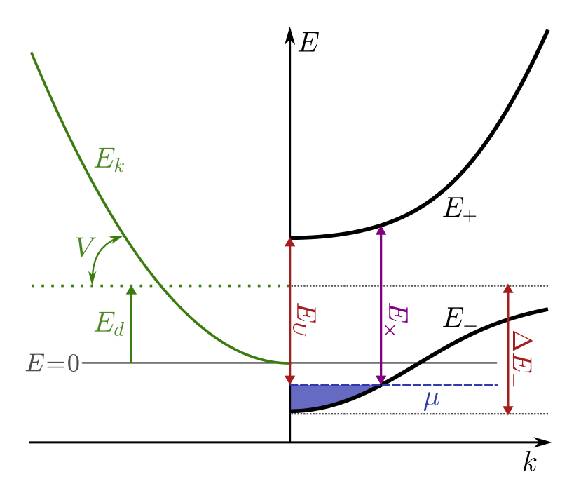
HMAs are a class of semiconductor alloys where the alloying elements have very different electronegativity than that of the host. Shan et al. described that localized states form around the mismatching elements and proposed a band anticrossing (BAC) model, which successfully describes the energy spectrum of HMAs Shan et al. (1999). According to the BAC model, the localized level and the host conduction band (CB) with dispersion hybridize at each wavevector independently with a single coupling factor (see Fig. 1). Two split bands emerge, with dispersion
| (1) |
where is the alloy fraction of the mismatching element. The two split bands are shown as solid black curves in Fig. 1. Here we consider a class of HMAs where the localized level anticrosses with a parabolic CB with , the bottom of which is taken to be the zero energy level, as shown in Fig. 1. All such HMAs are described by three scalar parameters: , , and .
We now describe the range of excitation energies that can be lost to particle-hole excitations in a doped HMA. We consider that the excess electrons occupy the band, and we consider zero temperature, so the chemical potential lies somewhere in , as in Fig. 1. The free electrons in produce plasmonic behavior Allami and Krich (2021) while at the same time providing two channels for dissipating energy. First, an excitation of any amount of energy up to the bandwidth of the band can move an electron from a filled state to an empty state within the band. The excited electron and hole can then dissipate their energy into a set of excitations with infinitesimal energy by moving electrons near the Fermi surface to nearby empty states. Figure 2 shows the range of excitation energies and where dissipation into particle-hole excitations can occur; the grey area under the horizontal dashed red line represents this intraband lossy region. Second, an electron can be excited to the band. The minimum energy for such interband transitions is , which is labeled in Figs. 1 and 2. Excitations with energy higher than can then be lost through a combination of inter- and intra-band transitions. The grey area above the slanted dashed line in Fig. 2 represents this second lossy region.
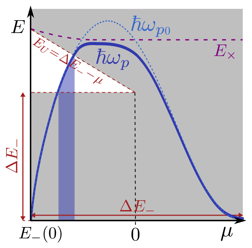
Excitations with energy between and are lossless, i.e., have no single-particle decay channels, if . The white area in Fig. 2 shows this lossless window, which linearly shrinks with increasing . Measuring energies from the bottom of , it turns out that , so . So there is always a lossless window if . Moreover, since the minimum of is always negative, for any HMA there is always a doping level below which there exists a lossless window.
The next step is to check when the plasmon energy falls in the lossless window. depends on the carrier concentration and hence on , which ranges between the bottom and the top of at zero temperature. As shown by the blue curve in Fig. 2, initially rises with as free carriers enter the band and falls back to zero when the band is full Allami and Krich (2021). Depending on the HMA parameters, can fall in the lossless window for some range of doping, as in the case in the figure.
In previous work Allami and Krich (2021), we found that for this class of HMAs obeys
| (2) |
in which is the plasma frequency in the absence of interband transitions, and the second term in the bracket represents the effect of interband transitions, where is a length scale that determines the strength of the transitions, which needs to be determined for each HMA. We provide more details in Section A of the supplementary material. Ref. Allami and Krich, 2021 derived a closed algebraic form for and an integral for , which is always positive and diverges as approaches , where is the Fermi momentum. Therefore, is bounded by and , as Fig. 2 shows. Note that since is the minimum distance between and the filled part of at the same , it is always larger than , which does not have the same restriction (see Figs. 1 and 2).
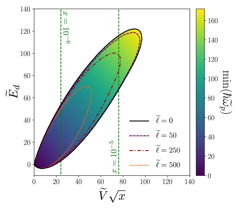
If we normalize all energies to , then we can accommodate this entire class of HMAs in a 2D plane spanned by and . But since for typical semiconductors is of the order of MeV, while meV is a more relevant unit for typical and , we normalize energies using and define , . For the bare electron mass , meV, so for any other effective mass one can scale all dimensionless energies by to find the approximate value in meV.
We can determine for any point in the plane whether there is a doping range in which falls in the lossless window, realizing lossless plasmons. Then, with fixed , where is the reduced Compton wavelength, there is a universal contour in the plane within which such HMAs fall. Fig. 3 shows these universal contours of lossless plasmonic HMAs for a few values of . The solid black contour shows the case without interband transitions, where . The contours do not vary significantly from the case until since in Eq. (2) is significant only for near . But since in the lossless window , the interband processes can move away from only when is large. For estimated typical values of Å, . Using in place of , as in the case, allows us to derive an analytic expression for the lossless contour, which is presented in Section B of the supplementary material.
The color scale of Fig. 3 shows the smallest in the lossless window. As Fig. 2 shows, the minimum value of in the lossless window is always , which does not depend on . Therefore, is the same for lossless contours belonging to different . Although the largest in the lossless window is somewhat different for each , the typical difference between and is of the order of a few for all cases.
Since , Fig. 3 shows that HMAs with heavier can achieve lossless plasmons for a wider range of and . Since the typical values of are on the order of eV, increasing the range of is particularly crucial because otherwise the required may be too small to realistically show alloying effects.
To illustrate this point, consider the quaternary HMA, Zn1-yCdyTe1-xOx, in which oxygen is the mismatching element in ZnCdTe. Table 1 shows the range of BAC parameters for this quaternary, determined from studies of alloy-dependent band gap.Tanaka et al. (2016); Adachi (2005) Doping of the band with chlorine has been demonstrated Tanaka et al. (2019), and this system can realize different values of by tuning the cadmium content . The range covered in Fig. 3 corresponds to between 0.27 and 0.29. The two nearly vertical dashed green lines in Fig. 3 show the locus of ZnCdTeO in the HMA parameter space, as varies for two fixed values of oxygen fraction, and , with details of the assumed bowing parameters described in Section C of the supplementary material. This range of , which produces near zero, allows overlap of with the lossless region when is sufficiently small. As the smallest for which the BAC model applies is unexplored, it is not clear whether these particular parameter ranges are experimentally realizable. ZnCdTe has , so in the lossless window we find from 3 to 6 meV for and 13 to 16 meV for . For these small , phonons could directly couple to the plasmons, providing a new channel for dissipation and breaking the lossless condition. A material with a heavier effective mass would allow both for larger and lossless plasmons with higher .
Observing these low plasma frequencies may require low temperatures, as Eq. (2) is derived at . At higher temperatures, the occupation fraction of states in the band must be taken into account. Nonetheless, the suppression of electronic decay channels in this lossless window should still be visible in experiments.
| Parameters | ||
|---|---|---|
| [eV] | -0.27 | 0.38 |
| [eV] | 2.8 | 2.2 |
| [] | 0.117 | 0.09 |
Although overall HMAs with heavier are more promising in realizing lossless plasmons, not everything favors them. Interband transitions shrink the lossless contour, as shown in Fig. 3, and increases linearly with . Lighter can allow smaller and a larger lossless contour.
The two most explored classes of conduction band HMAs are III-V nitrides and II-VI oxides Walukiewicz and Zide (2020).
Given the low effective masses of the conduction bands in these materials, the lossless plasmonic window will occur for THz-frequency with extremely light alloying.
As new HMAs with larger effective masses in their host bands are found, they will provide further opportunities to realize lossless plasmonic materials.
HMAs with valence band anticrossings Zhang et al. (2019); Pačebutas et al. (2019) could be good candidates, as they typically have heavier effective masses, though the theory of their plasmon frequencies has not yet been worked out.
HMAs present exciting potential for realizing a lossless plasmonic medium and are worth more theoretical and experimental investigations.
See the supplementary material for the details of the plasma frequency equation,
the analytic expression of the lossless contour for the case of ,
and the locus of ZnCdTeO in the HMA parameter space.
We acknowledge funding from the NSERC CREATE TOP-SET program, Award Number 497981.
author declarations
Conflict of Interest
The authors have no conflicts to disclose.
data availability
The data that support the findings of this study are openly available at https://github.com/hassan-allami/Lossless-HMAs Allami (2022).
Appendix A Deriving Eq. (2) for the plasma frequency
Eq. (2) of the main text is the rewriting of Eq. (20) of Ref. Allami and Krich, 2021. In Ref. Allami and Krich, 2021, is defined in Eq. (18) in terms of . By solving for , one can find . This form allows rewriting Eq. (18) of Ref. Allami and Krich, 2021 to give as
| (3) |
where is the fine structure constant.
The dimensionless can be expressed as
| (4) |
where all energies are in units of and all wavevectors are in units of . This form shows that is proportional to , so it is generally small except near where it diverges. It diverges at the smallest where for some in the integration domain, which motivates the definition of .
Appendix B Finding the lossless contour without interband transitions
To find the lossless contour for the case of , we need to find the set of HMA parameters for which falls in the lossless window for any . As Fig. 2 shows, has a maximum. We start by locating this maximum point . It is more convenient to find the maximum point for , which is also . We define and . Then using Eq. (3) to solve gives, after dividing out constants,
| (5) |
Since the largest in the lossless window is (see Fig. 2), we must find whether is negative.
When , note from Eq. (5) that when , which is the right edge of the lossless window, the sign of Eq. (5) is determined by the sign of . So if . In this case . Note that the lossless window is open only for and requires , so in this case can fall inside the window if . Therefore, if , the lossless plasmonic region in the HMA parameter space is determined by
| (6) |
where we used Eq. (3) for , and , which can be derived from Eq. (1).
When and hence , then the lossless window is open at , so falls in the lossless window when . For , we always have , because must fall within the band and is the top of the band.
To find , notice that is zero only when is at the bottom or top of the band, where . Then Eq. 5 says that is determined by the real roots of . This term always has two real roots, and only one of them corresponds to a inside the band. Picking the relevant root and using , we obtain
| (7) | ||||
Appendix C BAC parameters of Zn1-yCdyTe1-xOx
Table 1 shows the BAC parameters of Zn1-yCdyTe1-xOx for and extracted primarily from optical measurements Wełna et al. (2015); Yu et al. (2004); Seong, Miotkowski, and Ramdas (1998); Tanaka et al. (2016); Adachi (2005). We include bowing for using , with eV Samanta, Sharma, and Chaudhuri (1995); Tanaka et al. (2016), while for and , we used linear interpolation between the values shown in Table I.
The two dashed green lines in Fig. 3 show the locus of ZnCdTeO for two different fractions of oxygen as changes. The lines are not perfectly vertical, but they are nearly so because varies much less than for the same range of . Also, both and decrease with a similar rate as increases, leaving nearly unchanged.
references
References
- Ritchie (1957) R. H. Ritchie, “Plasma losses by fast electrons in thin films,” Phys. Rev. 106, 874–881 (1957).
- Powell and Swan (1960) C. J. Powell and J. B. Swan, “Effect of oxidation on the characteristic loss spectra of aluminum and magnesium,” Phys. Rev. 118, 640–643 (1960).
- Maier et al. (2007) S. A. Maier et al., Plasmonics: fundamentals and applications, Vol. 1 (Springer, 2007).
- Barnes, Dereux, and Ebbesen (2003) W. L. Barnes, A. Dereux, and T. W. Ebbesen, “Surface plasmon subwavelength optics,” Nature 424, 824–830 (2003).
- Ozbay (2006) E. Ozbay, “Plasmonics: Merging photonics and electronics at nanoscale dimensions,” Science 311, 189–193 (2006).
- Urbas et al. (2016) A. M. Urbas, Z. Jacob, L. D. Negro, N. Engheta, A. D. Boardman, P. Egan, A. B. Khanikaev, V. Menon, M. Ferrera, N. Kinsey, C. DeVault, J. Kim, V. Shalaev, A. Boltasseva, J. Valentine, C. Pfeiffer, A. Grbic, E. Narimanov, L. Zhu, S. Fan, A. Alù, E. Poutrina, N. M. Litchinitser, M. A. Noginov, K. F. MacDonald, E. Plum, X. Liu, P. F. Nealey, C. R. Kagan, C. B. Murray, D. A. Pawlak, I. I. Smolyaninov, V. N. Smolyaninova, and D. Chanda, “Roadmap on optical metamaterials,” J. Opt. 18, 093005 (2016).
- Kauranen and Zayats (2012) M. Kauranen and A. V. Zayats, “Nonlinear plasmonics,” Nat. Photonics 6, 737–748 (2012).
- Guo et al. (2013) X. Guo, Y. Ma, Y. Wang, and L. Tong, “Nanowire plasmonic waveguides, circuits and devices,” Laser Photonics Rev. 7, 855–881 (2013).
- Han and Bozhevolnyi (2012) Z. Han and S. I. Bozhevolnyi, “Radiation guiding with surface plasmon polaritons,” Rep. Prog. Phys. 76, 016402 (2012).
- Stockman (2010) M. I. Stockman, “The spaser as a nanoscale quantum generator and ultrafast amplifier,” J. Opt. 12, 024004 (2010).
- Atwater and Polman (2011) H. A. Atwater and A. Polman, “Plasmonics for improved photovoltaic devices,” in Materials for Sustainable Energy (World Scientific, 2011) pp. 1–11.
- Li, Cushing, and Wu (2015) M. Li, S. K. Cushing, and N. Wu, “Plasmon-enhanced optical sensors: a review,” Analyst 140, 386–406 (2015).
- Hou and Cronin (2013) W. Hou and S. B. Cronin, “A review of surface plasmon resonance-enhanced photocatalysis,” Adv. Funct. Mater. 23, 1612–1619 (2013).
- Fleischmann, Hendra, and McQuillan (1974) M. Fleischmann, P. Hendra, and A. McQuillan, “Raman spectra of pyridine adsorbed at a silver electrode,” Chem. Phys. Lett. 26, 163–166 (1974).
- Tame et al. (2013) M. S. Tame, K. McEnery, Ş. Özdemir, J. Lee, S. A. Maier, and M. Kim, “Quantum plasmonics,” Nat. Phys. 9, 329–340 (2013).
- Jiang et al. (2020) X. Jiang, P. Chen, K. Qian, Z. Chen, S. Xu, Y.-B. Xie, S. Zhu, and X. Ma, “Quantum teleportation mediated by surface plasmon polariton,” Sci. Rep. 10, 1–8 (2020).
- Boriskina et al. (2017) S. V. Boriskina, T. A. Cooper, L. Zeng, G. Ni, J. K. Tong, Y. Tsurimaki, Y. Huang, L. Meroueh, G. Mahan, and G. Chen, “Losses in plasmonics: from mitigating energy dissipation to embracing loss-enabled functionalities,” Adv. Opt. Photon. 9, 775–827 (2017).
- Khurgin and Boltasseva (2012) J. B. Khurgin and A. Boltasseva, “Reflecting upon the losses in plasmonics and metamaterials,” MRS Bull. 37, 768–779 (2012).
- Khurgin and Sun (2011) J. B. Khurgin and G. Sun, “Scaling of losses with size and wavelength in nanoplasmonics and metamaterials,” Appl. Phys. Lett. 99, 211106 (2011).
- Khurgin (2015) J. B. Khurgin, “How to deal with the loss in plasmonics and metamaterials,” Nat. Nanotechnol. 10, 2–6 (2015).
- Baffou and Quidant (2013) G. Baffou and R. Quidant, “Thermo-plasmonics: using metallic nanostructures as nano-sources of heat,” Laser Photonics Rev. 7, 171–187 (2013).
- Stockman et al. (2018) M. I. Stockman, K. Kneipp, S. I. Bozhevolnyi, S. Saha, A. Dutta, J. Ndukaife, N. Kinsey, H. Reddy, U. Guler, V. M. Shalaev, A. Boltasseva, B. Gholipour, H. N. S. Krishnamoorthy, K. F. MacDonald, C. Soci, N. I. Zheludev, V. Savinov, R. Singh, P. Groß, C. Lienau, M. Vadai, M. L. Solomon, I. Barton, David R., M. Lawrence, J. A. Dionne, S. V. Boriskina, R. Esteban, J. Aizpurua, X. Zhang, S. Yang, D. Wang, W. Wang, T. W. Odom, N. Accanto, P. M. de Roque, I. M. Hancu, L. Piatkowski, N. F. van Hulst, and M. F. Kling, “Roadmap on plasmonics,” J. Opt. 20, 043001 (2018).
- Wu et al. (2014) Y. Wu, C. Zhang, N. M. Estakhri, Y. Zhao, J. Kim, M. Zhang, X. Liu, G. K. Pribil, A. Alù, C. Shih, and X. Li, “Intrinsic optical properties and enhanced plasmonic response of epitaxial silver,” Adv. Mater. 26, 6106–6110 (2014).
- Stockman (2011) M. I. Stockman, “Nanoplasmonics: past, present, and glimpse into future,” Opt. Express 19, 22029–22106 (2011).
- Luk’yanchuk et al. (2010) B. Luk’yanchuk, N. I. Zheludev, S. A. Maier, N. J. Halas, P. Nordlander, H. Giessen, and C. T. Chong, “The fano resonance in plasmonic nanostructures and metamaterials,” Nat. Mater. 9, 707–715 (2010).
- Naik, Shalaev, and Boltasseva (2013) G. V. Naik, V. M. Shalaev, and A. Boltasseva, “Alternative plasmonic materials: beyond gold and silver,” Adv. Mater. 25, 3264–3294 (2013).
- West et al. (2010) P. West, S. Ishii, G. Naik, N. Emani, V. Shalaev, and A. Boltasseva, “Searching for better plasmonic materials,” Laser Photonics Rev. 4, 795–808 (2010).
- Naik et al. (2012a) G. V. Naik, J. Liu, A. V. Kildishev, V. M. Shalaev, and A. Boltasseva, “Demonstration of Al:ZnO as a plasmonic component for near-infrared metamaterials,” P. Natl. A. Sci. 109, 8834–8838 (2012a).
- Naik et al. (2012b) G. V. Naik, J. L. Schroeder, X. Ni, A. V. Kildishev, T. D. Sands, and A. Boltasseva, “Titanium nitride as a plasmonic material for visible and near-infrared wavelengths,” Opt. Mater. Express 2, 478–489 (2012b).
- Law et al. (2012) S. Law, D. C. Adams, A. M. Taylor, and D. Wasserman, “Mid-infrared designer metals,” Opt. Express 20, 12155–12165 (2012).
- Jung, Ustinov, and Anlage (2014) P. Jung, A. V. Ustinov, and S. M. Anlage, “Progress in superconducting metamaterials,” Supercond. Sci. Technol. 27, 073001 (2014).
- Khurgin and Sun (2010) J. B. Khurgin and G. Sun, “In search of the elusive lossless metal,” Appl. Phys. Lett. 96, 181102 (2010).
- Kim (2019) H. Kim, “Novel plasmon resonances of nonstoichiometric alumina,” Appl. Surf. Sci. 488, 648–655 (2019).
- Gjerding, Pandey, and Thygesen (2017) M. N. Gjerding, M. Pandey, and K. S. Thygesen, “Band structure engineered layered metals for low-loss plasmonics,” Nat. Commun. 8, 1–8 (2017).
- Khurgin (2017) J. B. Khurgin, “Mitigating the loss in plasmonics and metamaterials,” Tech. Rep. (Johns Hopkins University Baltimore United States, 2017).
- Saha, Shakouri, and Sands (2018) B. Saha, A. Shakouri, and T. D. Sands, “Rocksalt nitride metal/semiconductor superlattices: A new class of artificially structured materials,” Appl. Phys. Rev. 5, 021101 (2018).
- Shan et al. (1999) W. Shan, W. Walukiewicz, J. W. Ager, E. E. Haller, J. F. Geisz, D. J. Friedman, J. M. Olson, and S. R. Kurtz, “Band anticrossing in GaInNAs alloys,” Phys. Rev. Lett. 82, 1221–1224 (1999).
- Allami and Krich (2021) H. Allami and J. J. Krich, “Plasma frequency in doped highly mismatched alloys,” Phys. Rev. B 103, 035201 (2021).
- Tanaka et al. (2016) T. Tanaka, K. Mizoguchi, T. Terasawa, Y. Okano, K. Saito, Q. Guo, M. Nishio, K. M. Yu, and W. Walukiewicz, “Compositional dependence of optical transition energies in highly mismatched Zn1-xCdxTe1-yOy alloys,” Appl. Phys. Express 9, 021202 (2016).
- Adachi (2005) S. Adachi, Properties of group-IV, III-V and II-VI semiconductors (John Wiley & Sons, 2005) Chap. 7, p. 150.
- Tanaka et al. (2019) T. Tanaka, K. Matsuo, K. Saito, Q. Guo, T. Tayagaki, K. M. Yu, and W. Walukiewicz, “Cl-doping effect in ZnTe1-xOx highly mismatched alloys for intermediate band solar cells,” J. Appl. Phys. 125, 243109 (2019).
- Walukiewicz and Zide (2020) W. Walukiewicz and J. M. O. Zide, “Highly mismatched semiconductor alloys: From atoms to devices,” J. Appl. Phys. 127, 010401 (2020).
- Zhang et al. (2019) J. Zhang, Y. Wang, S. Khalid, A. Janotti, G. Haugstad, and J. M. O. Zide, “Strong band gap reduction in highly mismatched alloy InAlBiAs grown by molecular beam epitaxy,” J. Appl. Phys. 126, 095704 (2019).
- Pačebutas et al. (2019) V. Pačebutas, S. Stanionytė, R. Norkus, A. Bičiūnas, A. Urbanowicz, and A. Krotkus, “Terahertz pulse emission from GaInAsBi,” J. Appl. Phys. 125, 174507 (2019).
- Allami (2022) H. Allami, “Lossless HMAs,” (2022).
- Wełna et al. (2015) M. Wełna, R. Kudrawiec, Y. Nabetani, T. Tanaka, M. Jaquez, O. D. Dubon, K. M. Yu, and W. Walukiewicz, “Effects of a semiconductor matrix on the band anticrossing in dilute group II-VI oxides,” Semicond. Sci. Technol. 30, 085018 (2015).
- Yu et al. (2004) K. M. Yu, W. Walukiewicz, W. Shan, J. Wu, J. W. Beeman, M. A. Scarpulla, O. D. Dubon, and P. Becla, “Synthesis and optical properties of II-O-VI highly mismatched alloys,” J. Appl. Phys. 95, 6232–6238 (2004).
- Seong, Miotkowski, and Ramdas (1998) M. J. Seong, I. Miotkowski, and A. K. Ramdas, “Oxygen isoelectronic impurities in znte: Photoluminescence and absorption spectroscopy,” Phys. Rev. B 58, 7734–7739 (1998).
- Samanta, Sharma, and Chaudhuri (1995) B. Samanta, S. Sharma, and A. Chaudhuri, “Study of the microstructure and optical properties of polycrystalline Cd1-xZnxTe thin films,” Vacuum 46, 739–743 (1995).