Current address: ]Institute of Experimental Physics, Faculty of Physics, University of Warsaw, ul. Pasteura 5, PL-02-093 Warsaw, Poland
Current address: ]National High Magnetic Field Laboratory, Los Alamos National Laboratory, Los Alamos, NM 87545, USA
Disentangling electrical switching of antiferromagnetic NiO using high magnetic fields
Abstract
Recent demonstrations of the electrical switching of antiferromagnets (AFs) have given an enormous impulse to the field of AF spintronics. Many of these observations are plagued by non-magnetic effects that are very difficult to distinguish from the actual magnetic ones. Here, we study the electrical switching of thin () \ceNiO films in \cePt/NiO devices using magnetic fields up to to quantitatively disentangle these magnetic and non-magnetic effects. We demonstrate that these fields suppress the magnetic components of the electrical switching of \ceNiO, but leave the non-magnetic components intact. Using a monodomainization model the contributions are separated, showing how they behave as a function of the current density. These results show that combining electrical methods and strong magnetic fields can be an invaluable tool for AF spintronics, allowing for implementing and studying electrical switching of AFs in more complex systems.
Recently, there has been a lot of attention for controlling the magnetic order of antiferromagnetic materials. The insensitivity to external magnetic fields, combined with -frequency magnetization-dynamics, makes antiferromagnets interesting for numerous applications, ranging from data-storage devices [1] to radiation sources [2, 3, 4]. However, control over the orientation of the magnetic order in an antiferromagnet remains problematic, and it has only recently been demonstrated that the magnetic order can be controlled using electrical currents [5, 6]. Since these first demonstrations, there have been many experiments that manipulate the antiferromagnetic state in a variety of systems, such as multi-layer systems with antiferromagnets and ferromagnets [7, 8], or systems with non-collinear antiferromagnets [9, 10].
In insulating antiferromagnets, such as \ceNiO, \ceCoO, and \ceFe2O3, experiments have shown that the magnetic order can be controlled using electrical current pulses through an adjacent heavy metal (e.g. \cePt) [6, 11, 12, 13]. The current in the heavy metal layer is, via the spin-Hall effect, converted into a transverse spin current. In turn, this spin current is injected into the antiferromagnet where it exerts a spin-torque on the spins, which is then expected to manipulate the magnetic order of the antiferromagnet [6, 14]. Alternatively, Joule heating due to the current pulse can give rise to a thermomagnetoelastic effect, which can change the anisotropy of the antiferromagnet sufficiently to induce a change in the antiferromagnetic order [15].
However, recently there has been a debate about the actual origin of the signals observed in the above-mentioned electrical switching experiments, as they can equally well be explained by non-magnetic, parasitic effects, such as structural changes or damage caused by Joule heating, or electromigration [16, 17, 18, 12]. Although there are demonstrations that show with certainty that actual magnetic reorientation is possible, it is generally difficult to distinguish between the magnetic and non-magnetic contributions to the electrical switching signals, as the electrical measurements themselves consist only of Hall measurements showing the electrically-induced switching as an up-down pattern. This shortcoming can be resolved using imaging techniques that can resolve the magnetic state of an antiferromagnet, such as XMLD-PEEM [14, 19]. However, this requires an X-ray beam-line and is limited to devices with relatively free access to the antiferromagnet in question, i.e. devices where the antiferromagnetic layer is not buried beneath other layers.
Here we disentangle magnetic and non-magnetic effects in the electrical switching of thin films of \ceNiO using strong magnetic fields of up to . If the magnetic field is stronger than the monodomainization field (determined to be for our samples, Supplemental Material [20]) the magnetic order of \ceNiO is organized in a single domain, whose magnetic orientation is controlled by the external magnetic field [21]. Hence, the effect of reorienting the magnetic moments in an electrical switching experiment is expected to be suppressed in such a field. As Joule heating and electromigration are not affected by the magnetic field, they will therefore remain present, giving a way to disentangle the magnetic and non-magnetic contributions.
We show that it is indeed possible to suppress the electrical switching effects in \cePt/NiO devices by applying a sufficiently strong magnetic field of over . Field dependence of the switching signal is observed and can be understood and modelled with a multi-domain interpretation of the NiO magnetic structure [21]. Using this model, we demonstrate that the magnetic and non-magnetic contributions to the observed switching signal can be separated from each other. Thereby, this technique helps to better understand the electrical switching experiments and allows integrating and investigating the electrical switching of antiferromagnets in more complex devices.
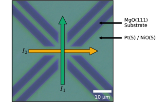
For these experiments, we fabricate eight-terminal devices as shown in Fig. 1 consisting of \ceNiO on top of a \cePt layer ( each) on \ceMgO(111) substrates. Both layers are grown using DC magnetron sputtering, at for the \cePt layer to ensure the crystallinity of the \cePt layer and at in a 10:1 \ceAr:\ceO-mixture for the \ceNiO layer. The quality of these layers is ensured using a variety of characterization techniques (Supplemental Material [20]). From these layers, devices as shown in Fig. 1 are fabricated using a combination of electron-beam lithography, electron-beam evaporation, lift-off, and ion-beam milling.
With these devices electrical switching experiments are performed, similar to the ones discussed in literature [6]. To switch the AF state, current pulses of are applied along the wide orthogonal current lines and , as indicated in Fig. 1 (the probe lines are also included when applying the pulses for a more homogeneous current distribution). After every pulse, the small diagonal current lines are used for probing the present state with a Hall measurement; an alternating probing current of (equivalent to a current density of ) at is passed in one direction and the generated Hall voltage is detected along the perpendicular current line using standard lock-in techniques. Typically, there is a delay of between a pulse and the subsequent probing.
These experiments are performed within a cryostat, enabling the control of the temperature, that is placed in the center of a superconducting magnet, allowing for fields up to to be applied in the plane of the sample, along one of the probing lines (i.e. along the directions that are rotated from the direction, approximately the and directions).
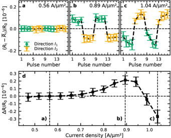
A typical experimental result of electrical switching in the absence of a magnetic field is shown in Fig. 2a-c. In the experiment, four current pulses are applied in one direction (), whereafter four pulses are applied along the perpendicular direction (). After each pulse, the Hall resistance along the small diagonal current lines is measured; for better comparison between different devices and temperatures, we subtract the average Hall resistance (averaged over the entire measurement) from the Hall resistance and normalize the value to the longitudinal resistance (typically around , but the exact value can differ between devices, measurements and temperatures). Changes of the Néel vector should show up in the Hall resistance since one of its contributions, the transverse component of the spin-Hall magnetoresistance (SMR), is sensitive to reorientations of the Néel vector of \ceNiO from to with respect to the direction of the probing current [22]. It is observed that for a specific pulse current density () the two different pulse directions result in two distinct values of the Hall resistance, which is expected if indeed the Néel vector of \ceNiO has been switched by by the current pulse. However, it should be noted that, as mentioned earlier, other, non-magnetic effects can give similar results.
Upon increasing the pulse amplitude, as shown in Fig. 2c, we find that the behavior changes from a step-like switching at to a sawtooth-like switching at , where each subsequent current pulse in a certain direction still contributes to the final resistance state. This sawtooth-like switching behavior also has an inverted sign when compared to the step-like switching at lower current densities; for lower current density the pulses marked in green result in a high relative resistance state and the orange in a lower state, whereas for higher current density the green pulses result in a low resistance state and the orange in a higher state. For lower current densities (see Fig. 2a for ) the resistance state is insensitive to the direction of the pulses; for this current density, no switching behavior is observed.
The total current density-dependent switching behavior is summarized in Fig. 2d, where the switching amplitude is plotted. This switching amplitude is defined as the difference between the (average) transverse resistance after a current pulse in either direction, i.e. ; for consistency between devices, all values are normalized by the longitudinal resistance of the device . Here it becomes clear that starting from a form of current-induced switching becomes visible, reaching a maximum at around . When the current density further increases, the switching amplitude starts to rapidly decrease, changes sign and increase again (in the negative direction).
This switching behavior, with the change of sign and the associated transition from step-like to sawtooth-like switching, indicates that there are at least two mechanisms at play in these experiments. As mentioned earlier, these mechanisms can be either magnetic or non-magnetic of origin [16, 17, 18]. However, from this set of measurements alone it is impossible to tell if one of the mechanisms involved in the experiment is or is not magnetic of origin, and if so, which part of the curve is explained by this magnetic mechanism.
To try to separate the magnetic from the non-magnetic effects, we perform an identical experiment in a superconducting magnet where magnetic fields up to can be reached. When a sufficiently strong magnetic field is applied to the sample, the Néel vector (or equivalently, the individual magnetic moments) of the \ceNiO layer will be forced in a configuration perpendicular to the magnetic field [23, 21]. Note that this resembles the state after a spin-flop transition; however, thin films of \ceNiO are known to rather undergo a monodomainization transition due to the relaxation of stress [21, 24]. Upon applying a current pulse in such a magnetic field, we conjecture that one of two things will happen. One possibility is that the current pulse will not be sufficiently strong to overcome the external magnetic field and influence the orientation of the Néel vector. Alternatively, if the current pulse can affect the orientation of the Néel vector despite the presence of a strong external magnetic field, we expect the new orientation of the Néel vector will be reverted to the field-dominated orientation after the current pulse has stopped since the magnetic field is strong enough to force an orthogonal 111Although the high magnetic fields that are used in these experiments are expected to cant the magnetic moments slightly away from a direction that is perfectly orthogonal to the external magnetic field, we estimate that this canting is sufficiently small ( at ) that this deviation can be disregarded in the interpretation of the experiments. orientation of the magnetic moments [23, 21].
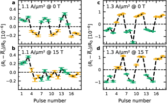
The results of these measurements are shown in Fig. 3, both for a medium current density (a and b) and for a higher current density (c and d). Note that these measurements have been performed at a different temperature ( rather than ). Since both the magnetic and non-magnetic effects are dependent on temperature [11], the exact current densities that are required to obtain the same switching patterns can differ between different temperatures. For this reduced temperature, a slightly higher current density is needed to obtain the same switching patterns as in Fig. 2; this is more thoroughly explored in the Supplemental Information [20].
Similar to the previous measurements (Fig. 2) we can see that the current pulses along the different directions ( and ) result in a switching pattern. Please note that the high magnetic field setup results in a higher noise level in the measurements leading to a bit more irregular patterns than in zero field; this has no impact on the conclusions of this work as these are based only on the general difference between the two current directions. When comparing the zero field experiment (Fig. 3a) to the high field experiment (, Fig. 3b) for the medium current density, we observe that the switching behavior that is visible at zero field is absent for the high field experiment. For the high current density (Fig. 3 c and d, respectively) no such trend is observed; for both zero and high magnetic fields, switching behavior is observed.
As the electrical switching of \ceNiO is expected to be suppressed by a high magnetic field, we conjecture that the behavior we observe at medium current density is indeed caused by a magnetic effect; the switching behavior at higher current densities is then caused by non-magnetic effects as these are not expected to be affected by the magnetic field. Note, however, that these two effects are not mutually exclusive and may have a gradual transition from one to the other. Hence, it is possible that in the high current density regime there is a small magnetic component, and that in the medium current density regime there is a small non-magnetic component.
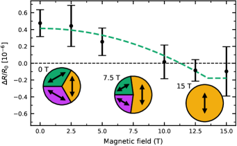
To better identify these small contributions, we plot the switching amplitudes as a function of the external magnetic field magnitude in Fig. 4 for the medium current density. In this figure, the dependence of the switching amplitude on the external magnetic field is visible. At low magnetic fields, the switching amplitude is nearly unperturbed by the external magnetic field. However, towards higher magnetic fields the switching amplitude is greatly reduced until it reaches a plateau around .
We conjecture that this behavior demonstrates the presence of two entangled contributions, the magnetic one that gets suppressed by the high field and the non-magnetic one that can be associated with the plateau that is reached at high fields. To substantiate this hypothesis, modelling of the population of the antiferromagnetic domains for \ceNiO in high magnetic fields, and the resulting SMR is needed; for this, we make use of the monodomainization model [21].
The model describes the \ceNiO(111) layer of our samples by separating it into three domains, where the Néel vectors of the three domains are separated by (corresponding to the three spin domains in the \ceNiO(111) plane [26]); in Fig. 4 this distribution is represented in pie-charts. While this interpretation and the analytical expressions that are derived from the model are based on \ceNiO(111) having three domains, the results are also valid in cases where the system has more (or equivalently, less well-defined) domains (Supplemental Material [20]), as is expected for the thin film of \ceNiO in our samples [24].
In low magnetic fields, due to de-stressing, each of the domains takes up approximately an equal portion of the sample. When a strong magnetic field is applied, the distribution of these domains changes due to the Zeeman energy, where the domain with (the largest projection of) the Néel vector perpendicular to the external magnetic field are preferred; this domain will increase in size at the cost of the other domains. Finally, if the magnetic field surpasses the monodomainization field , there is only a single domain left, namely the domain with the Néel vector perpendicular to the external magnetic field.
This behavior results in a field-dependent transverse spin-Hall magnetoresistance (SMR) that is given by [21]:
| (1) |
In the electrical switching experiments, it is expected that only a small portion of the magnetic structure is actually switched between the available domains upon applying a current pulse [24]. However, when an external magnetic field is applied and the distribution of domains changes, fewer domains are available to switch between. Therefore, we assume that the magnetic contribution to the switching signal scales as . An additional field-independent offset has been added to account for non-magnetic effects that are expected to contribute to the measured switching amplitude. When combined with Eq. 1, the switching amplitude can then be expressed as:
| (2) |
where is the SMR proportionality constant that accounts for the contribution of the changes in the antiferromagnetic state to the measured switching amplitude.
To fit the model to the data, the monodomainization field [20] is kept constant and only and are varied. As shown in Fig. 4, the fitted curve follows the data closely and emphasizes the gradual suppression of the magnetic contribution up to the monodomainization field and the non-magnetic plateau for higher fields.
As we now understand the field dependence of the switching amplitude , it can be used to help settle the debate regarding the contributions of the magnetic and non-magnetic, parasitic effects to the observed switching signal. To directly connect to the earlier discussed current dependence (Fig. 2), we repeat the switching in high magnetic field experiments for a series of current densities. By fitting the monodomainization model (Eq. 2) to the measurements at every current density, a measure for both the magnetic () and the non-magnetic () contribution to the signal at zero magnetic field can be obtained.
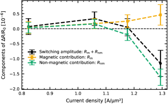
In Fig. 5 these separate contributions are plotted as a function of the current density of the pulses. Here, it can be noted that the magnetic component slowly increases with increasing current density. Simultaneously it is observed that the non-magnetic part rises (with an opposite sign from the magnetic part) from to ; for higher current densities, however, it changes sign and the magnitude rises strongly in a non-linear manner, which hints at a thermal origin of this effect [11].
The sum of the two contributions shows (qualitatively) the same behavior as the switching amplitude at zero magnetic field (Fig. 2d), despite a small mismatch in temperature ( for Fig. 2d compared to for Fig. 5, related to different temperature control possibilities in the different setups). For medium current densities, this indicates that the observed (step-like) switching signal (e.g. Fig. 2b) is a combination of both magnetic and non-magnetic components. At high current densities (e.g. Fig. 2c), the (sawtooth-like) switching signal is mostly a result of the non-magnetic contributions; the inverted sign of this switching signal is also a consequence of these non-magnetic effects. These conclusions are in line with earlier interpretations [14, 12] that the step-like switching can often be attributed to magnetic effects and sawtooth-like switching to non-magnetic effects.
We are convinced—in particular, based on the agreement with the expected behavior and the high magnetic field, typical for antiferromagnetic \ceNiO, needed to suppress the switching—that these results show that we are indeed able to separate the magnetic and non-magnetic effects using high magnetic fields. Additional control experiments could be performed to further support these conclusions; to enable a meaningful comparison with the present data, a careful detailed analysis of results from non-magnetic control samples would be required.
In summary, we have investigated the field-dependence of the electrical switching of \ceNiO to distinguish between the magnetic and non-magnetic contributions to the electrical switching experiments. We showed that for lower current densities the (step-like) switching pattern is greatly suppressed upon applying a high magnetic field. For higher current densities, on the other hand, the (inverted, sawtooth-like) switching pattern remains largely unaffected by the magnetic field, hinting at a non-magnetic origin.
Using a monodomainization model the magnetic and non-magnetic contributions can be separated from each other. This confirmed that the switching at lower current densities is in part due to actual magnetic switching of \ceNiO; however, also at these lower current densities, a non-magnetic contribution is present. Moreover, it showed that the change-of-sign that is observed at higher current densities is caused by non-magnetic effects; for these higher current densities there is still a magnetic part (which is slightly stronger than the magnetic effects at lower current densities) but the non-magnetic component dominates the signal.
We have shown that a strong magnetic field can be used to quantitatively disentangle magnetic and non-magnetic effects in experiments aiming at the electrical switching experiments of antiferromagnets. This technique relieves the necessity for imaging the antiferromagnetic structure as a way to study the electrical switching of antiferromagnets and thereby opens a way to investigate more complex devices where the antiferromagnetic layer is just one of the many layers and imaging of the antiferromagnetic domains becomes increasingly difficult or impossible.
Acknowledgements.
We acknowledge S. Peeters for measuring the sheet resistance of an unpatterned sample. Sample fabrication was performed using NanoLabNL facilities. The research performed here was funded by the Dutch Research Council (NWO) under grant No. 680-91-113. This work was supported by HFML-RU/NWO-I, member of the European Magnetic Field Laboratory (EMFL). C.F.S. and M.J.G. conceived the experiments, fabricated the samples with help from T.J.K., and performed the measurements while advised by H.J.M.S. High magnetic field experiments were performed by C.F.S. and M.J.G. with help from K.R. and M.E.B. while advised by U.Z. C.F.S. performed the data analysis while advised by M.J.G., H.J.M.S., and R.D.References
- Jungwirth et al. [2016] T. Jungwirth, X. Marti, P. Wadley, and J. Wunderlich, Antiferromagnetic spintronics, Nature Nanotechnology 11, 231 (2016).
- Khymyn et al. [2017] R. Khymyn, I. Lisenkov, V. Tiberkevich, B. A. Ivanov, and A. Slavin, Antiferromagnetic thz-frequency josephson-like oscillator driven by spin current, Scientific Reports 7, 43705 (2017).
- Stremoukhov et al. [2019] P. Stremoukhov, A. Safin, M. Logunov, S. Nikitov, and A. Kirilyuk, Spintronic terahertz-frequency nonlinear emitter based on the canted antiferromagnet-platinum bilayers, Journal of Applied Physics 125, 223903 (2019).
- Cheng et al. [2016] R. Cheng, D. Xiao, and A. Brataas, Terahertz antiferromagnetic spin hall nano-oscillator, Physical Review Letters 116, 207603 (2016).
- Wadley et al. [2016] P. Wadley, B. Howells, J. Železný, C. Andrews, V. Hills, R. P. Campion, V. Novák, K. Olejník, F. Maccherozzi, S. S. Dhesi, S. Y. Martin, T. Wagner, J. Wunderlich, F. Freimuth, Y. Mokrousov, J. Kuneš, J. S. Chauhan, M. J. Grzybowski, A. W. Rushforth, K. W. Edmonds, B. L. Gallagher, and T. Jungwirth, Electrical switching of an antiferromagnet, Science 351, 587 (2016).
- Chen et al. [2018] X. Z. Chen, R. Zarzuela, J. Zhang, C. Song, X. F. Zhou, G. Y. Shi, F. Li, H. A. Zhou, W. J. Jiang, F. Pan, and Y. Tserkovnyak, Antidamping-torque-induced switching in biaxial antiferromagnetic insulators, Physical Review Letters 120, 207204 (2018).
- Li et al. [2020] Y. Li, J. Liang, H. Yang, H. Zheng, and K. Wang, Current-induced out-of-plane effective magnetic field in antiferromagnet/heavy metal/ferromagnet/heavy metal multilayer, Applied Physics Letters 117, 092404 (2020).
- Liu et al. [2020] X. H. Liu, K. W. Edmonds, Z. P. Zhou, and K. Y. Wang, Tuning interfacial spins in antiferromagnetic–ferromagnetic–heavy-metal heterostructures via spin-orbit torque, Physical Review Applied 13, 014059 (2020).
- Tsai et al. [2020] H. Tsai, T. Higo, K. Kondou, T. Nomoto, A. Sakai, A. Kobayashi, T. Nakano, K. Yakushiji, R. Arita, S. Miwa, Y. Otani, and S. Nakatsuji, Electrical manipulation of a topological antiferromagnetic state, Nature 580, 608 (2020).
- Deng et al. [2021] Y. Deng, R. Li, and X. Liu, Thickness dependent anomalous hall effect in noncollinear antiferromagnetic mn3sn polycrystalline thin films, Journal of Alloys and Compounds 874, 159910 (2021).
- Grzybowski et al. [2022] M. J. Grzybowski, C. F. Schippers, M. E. Bal, K. Rubi, U. Zeitler, M. Foltyn, B. Koopmans, and H. J. M. Swagten, Electrical switching of antiferromagnetic coo | pt across the néel temperature, Applied Physics Letters 120, 122405 (2022).
- Cheng et al. [2020] Y. Cheng, S. Yu, M. Zhu, J. Hwang, and F. Yang, Electrical switching of tristate antiferromagnetic néel order in α-fe2o3 epitaxial films, Physical Review Letters 124, 027202 (2020).
- Moriyama et al. [2018] T. Moriyama, K. Oda, T. Ohkochi, M. Kimata, and T. Ono, Spin torque control of antiferromagnetic moments in nio, Scientific Reports 8, 14167 (2018).
- Baldrati et al. [2019] L. Baldrati, O. Gomonay, A. Ross, M. Filianina, R. Lebrun, R. Ramos, C. Leveille, F. Fuhrmann, T. R. Forrest, F. Maccherozzi, S. Valencia, F. Kronast, E. Saitoh, J. Sinova, and M. Kläui, Mechanism of néel order switching in antiferromagnetic thin films revealed by magnetotransport and direct imaging, Physical Review Letters 123, 177201 (2019).
- Meer et al. [2021] H. Meer, F. Schreiber, C. Schmitt, R. Ramos, E. Saitoh, O. Gomonay, J. Sinova, L. Baldrati, and M. Kläui, Direct imaging of current-induced antiferromagnetic switching revealing a pure thermomagnetoelastic switching mechanism in nio, Nano Letters 21, 114 (2021).
- Chiang et al. [2019] C. C. Chiang, S. Y. Huang, D. Qu, P. H. Wu, and C. L. Chien, Absence of evidence of electrical switching of the antiferromagnetic néel vector, Physical Review Letters 123, 227203 (2019).
- Churikova et al. [2020] A. Churikova, D. Bono, B. Neltner, A. Wittmann, L. Scipioni, A. Shepard, T. Newhouse-Illige, J. Greer, and G. S. D. Beach, Non-magnetic origin of spin hall magnetoresistance-like signals in pt films and epitaxial nio/pt bilayers, Applied Physics Letters 116, 022410 (2020).
- Matalla-Wagner et al. [2020] T. Matalla-Wagner, J.-M. Schmalhorst, G. Reiss, N. Tamura, and M. Meinert, Resistive contribution in electrical-switching experiments with antiferromagnets, Physical Review Research 2, 033077 (2020).
- Wadley et al. [2018] P. Wadley, S. Reimers, M. J. Grzybowski, C. Andrews, M. Wang, J. S. Chauhan, B. L. Gallagher, R. P. Campion, K. W. Edmonds, S. S. Dhesi, F. Maccherozzi, V. Novak, J. Wunderlich, and T. Jungwirth, Current polarity-dependent manipulation of antiferromagnetic domains, Nature Nanotechnology 13, 362 (2018).
- [20] See Supplemental Material at [URL will be inserted by publisher] for details on growth and characterization of the samples used in this work, the determination of the monodomainization field of the NiO samples, the validation of the monodomainization model for thin films of NiO, and the temperature dependence of the switching amplitude.
- Fischer et al. [2018] J. Fischer, O. Gomonay, R. Schlitz, K. Ganzhorn, N. Vlietstra, M. Althammer, H. Huebl, M. Opel, R. Gross, S. T. B. Goennenwein, and S. Geprägs, Spin hall magnetoresistance in antiferromagnet/heavy-metal heterostructures, Physical Review B 97, 014417 (2018).
- Chen et al. [2016] Y.-T. Chen, S. Takahashi, H. Nakayama, M. Althammer, S. T. B. Goennenwein, E. Saitoh, and G. E. W. Bauer, Theory of spin hall magnetoresistance (smr) and related phenomena, Journal of Physics: Condensed Matter 28, 103004 (2016).
- Machado et al. [2017] F. L. A. Machado, P. R. T. Ribeiro, J. Holanda, R. L. Rodríguez-Suárez, A. Azevedo, and S. M. Rezende, Spin-flop transition in the easy-plane antiferromagnet nickel oxide, Physical Review B 95, 104418 (2017).
- Gray et al. [2019] I. Gray, T. Moriyama, N. Sivadas, G. M. Stiehl, J. T. Heron, R. Need, B. J. Kirby, D. H. Low, K. C. Nowack, D. G. Schlom, D. C. Ralph, T. Ono, and G. D. Fuchs, Spin seebeck imaging of spin-torque switching in antiferromagnetic pt/nio heterostructures, Physical Review X 9, 041016 (2019).
- Note [1] Although the high magnetic fields that are used in these experiments are expected to cant the magnetic moments slightly away from a direction that is perfectly orthogonal to the external magnetic field, we estimate that this canting is sufficiently small ( at ) that this deviation can be disregarded in the interpretation of the experiments.
- Uchida et al. [1967] E. Uchida, N. Fukuoka, H. Kondoh, T. Takeda, Y. Nakazumi, and T. Nagamiya, Magnetic anisotropy of single crystals of nio and mno, Journal of the Physical Society of Japan 23, 1197 (1967).