Anomalous fractal scaling in two-dimensional electric networks
Abstract
Much of the qualitative nature of physical systems can be predicted from the way it scales with system size. Contrary to the continuum expectation, we observe a profound deviation from logarithmic scaling in the impedance of a two-dimensional circuit network. We find this anomalous impedance contribution to sensitively depend on the number of nodes in a curious erratic manner, and experimentally demonstrate its robustness against perturbations from the contact and parasitic impedance of individual components. This impedance anomaly is traced back to a generalized resonance condition reminiscent of the Harper’s equation for electronic lattice transport in a magnetic field, even though our circuit network does not involve magnetic translation symmetry. It exhibits an emergent fractal parametric structure of anomalous impedance peaks for different that cannot be reconciled with continuum theory and does not correspond to regular waveguide resonant behavior. This anomalous fractal scaling extends to the transport properties of generic systems described by a network Laplacian whenever a resonance frequency scale is simultaneously present.
I Introduction
From dimensional analysis to the universality of critical phase transitions, scaling theory provides a universal paradigm for the principal understanding of most physical phenomena [1, 2, 3, 4, 5, 6, 7]. Particularly interesting are “marginal” scenarios, where observables exhibit great freedom in their functional dependency on the physical variables [8, 9, 10, 11]. A classic example is the electrical impedance of a -dimensional sample of characteristic length , which scales as ; in particular, for , must scale slower than any power of , most commonly logarithmically.
Indeed, logarithmic scaling is ubiquitous in physics, appearing in a broad range of contexts as disparate as conformal field theory, disorder Green’s functions, strongly coupled quantum fields, and graph complexity [12, 13, 14, 15, 16]. It represents the paradigmatic slower-than-power-law behavior that appears naturally in various scale-free scenarios. Particularly, impedance scaling in electrical circuits, as a function of circuit size, dutifully displays this scaling behavior when the circuit is either entirely reactive or resistive. For instance, the dimensionality of lattice models determines whether the impedance scales linearly, logarithmically or saturates to a constant impedance value. While 1D and 2D samples exhibit these scaling characteristics such as linear or logarithmic scaling, the impedance in circuits characterized with dimensionality experiences rapid saturation proportional to . Nevertheless, although the dimensionality of the lattice delineates the scaling characteristics, it ceases to be the predominant determinant in heterogeneous resonant medias. In fact, the scaling profile of circuits with inductance and capacitance relies more on the form of the lattice array rather than the lattice dimension [17, 18]. This is because the impedance across two opposite farthest sites varies due to the parameter space irrespective of the lattice dimension. To explain this, we will conceptually elucidate and experimentally demonstrate the resonant conditions through a seemingly elementary physical 2D system by evaluating its corner-to-corner impedance behavior.
The two-point impedance and resistance problem has garnered significant attention [19, 20, 21, 22, 23, 24, 25, 26] as it not only allows for the study of electrical conductivity, but also serves as a means of uncovering new physical phenomena related to lattice dimension, network model, lattice uniformity, and boundary design from the changes in the electrical characteristics in the presence of perturbations or disorder [27, 28, 29, 30, 31]. The extensive research conducted in this expansive field has enhanced our fundamental understanding of electric circuits [32, 33, 34, 35, 36, 37, 38, 39, 40, 41, 42, 43, 44, 45, 33] and has practical applications in the design of various circuit systems, including topolectrical circuits [46, 47, 48, 49, 50, 51, 52], non-linear systems [53, 54, 55, 56], condensed matter counterparts [57, 58], and metamaterials [59]. In addition to numerical approaches such as the Laplacian formalism [60, 61, 62], various analytical methods have been developed for determining the two-point impedance, including the recursion-transform method [18, 63, 64, 65, 66, 67, 68], the lattice Green’s function [69, 70, 71, 72, 73, 74], asymptotic expansion [75, 76], and the method of images [77, 78]. While each of these methods employs a distinct approach to evaluate the impedance in both reactive and resonant media, they all require the circuit network to possess symmetries such as inversion and translation symmetries. The role of these symmetries has not been thoroughly explored in the literature, but their presence may result in anomalous behaviors that can be uncovered through the impedance scaling in electric circuits.
In this work, we report a dramatic uniform scaling violation in the impedance across circuit lattices, resulting from the suppression of current at the boundaries due to the circuit symmetries. To demonstrate this, we specifically examine a 2D square circuit, wherein its reactive counterpart displays a notable logarithmic scaling. Although the same qualitative picture can be observed in circuits with different dimensions, the 2D circuit allows us to investigate the origin of uniform scaling violations using a simpler yet richer example. Naively, one would expect from the impedance of a 2D circuit to vary smoothly with the number of unit cells from its continuum analogue since the circuit lattice can be construed as a discretization of 2D conducting plates. However, while this indeed holds for non-resonant circuits, such as those containing capacitors or resistors exclusively, the impedance behavior for resonant media i.e., circuits, cannot be more different. Our theoretical and experimental investigations reveal curious impedance enhancements of up to a few orders at certain lattice sizes , whose roots can be traced to a new commensurability criterion associated with a Hofstadter butterfly-like fractal structure. This challenges the applicability of a continuum description in even the simplest of resonant media.
II Results
II.1 Violation of logarithmic impedance scaling
To put our anomalous circuit impedance scaling behavior into perspective, we introduce the quantity , which is the fractional rate of change of the impedance with the system size . It is closely related to the -function in renormalization group analysis [79, 80, 81], and has also been famously employed in understanding the conductivity localization transition [82, 83, 84, 15, 85, 86] due to disorder scattering.
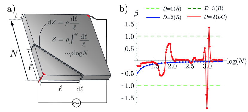
In most conductors where , we have a constant , which indicates that the impedance increases (decreases) with the system size in a consistent qualitative manner for (). This is the case for purely resistive media (such as the conducting plate depicted in Fig. 1a) for which the impedance scales logarithmically viz. , giving rise to as sketched in Fig. 1b (blue, green and dark green). However, we unveil that this crossover to the asymptotic limit can be far from smooth when a AC frequency scale exists in the circuit. As plotted in Fig. 1b (red) for an illustrative 2D AC circuit lattice (detailed later), fluctuates erratically and dramatically as the system size increases. (Note that the irregular impedance scaling depicted in red in Fig. 1b is not exclusive to a 2D sample but can occur in an lattice, regardless of their dimensions.) In the following sections, this anomalous scaling behavior will be revealed to be part of an intricate fractal-like characteristic with slightly different reactance parameters often giving rise to unpredictably distinct anomalous impedance scaling.
II.2 RLC Circuit with anomalous impedance scaling
We investigate the discretization of the simplest 2D conducting sample, which is a square lattice circuit array with fixed components connecting each node [Fig. 2a]. For consistency, we shall always measure the impedance across two diagonally opposite corner nodes, even though the subsequent results remain qualitatively valid for arbitrary impedance intervals. If every connection in the square lattice is composed of the same element , it can be shown (see Methods) that the corner-to-corner impedance scales like [Fig. 2d]. This is not surprising, since it is only natural to expect that the square circuit lattice inherits the same logarithmic scaling as its continuum counterpart.
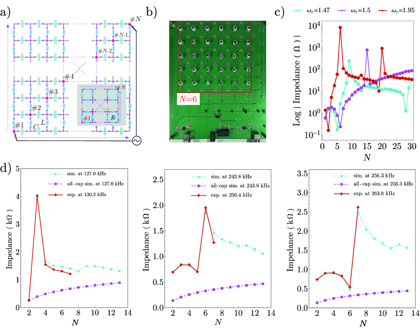
Yet, we find that this usual logarithmic impedance scaling becomes severely violated when the lattice connections are replaced by two different circuit components with impedance of opposite signs, such as and components, which define a frequency scale. Specifically, we built an square lattice circuit array on circuit boards [Fig. 2b] (), such that each horizontal link contains a capacitor and each vertical link contains an inductor . In momentum space, the circuit Laplacian , which relates the voltage and input current profiles via , takes the form
| (1) |
where denotes the AC driving frequency. Barring the overall prefactor, is the only nontrivial parameter of our circuit besides the lattice size , neither of which constitutes another competing length scale.
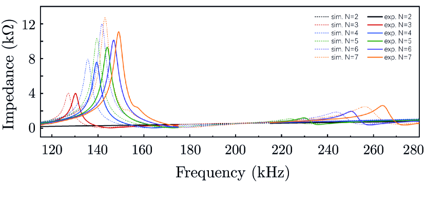
For a fixed , the measured corner-to-corner impedance does not follow a simple trend with the lattice size , but varies erratically with abrupt and prominent peaks at certain . As plotted in Fig. 2c for an ideal circuit without any dissipation, the impedance fluctuates wildly as is increased, such that can abruptly become a few orders of magnitude larger for particular values of . Besides, the impedance behaves qualitatively differently for different , even across small changes in . It is noteworthy that such “quasi-random” behavior is robustly measurable in an actual experimental implementation with inevitable dissipation, as reflected in our measured data (Fig. 2d), which agrees well with theory despite unavoidable parasite and contact resistances as well as component disorder.
II.3 Emergent fractal resonances
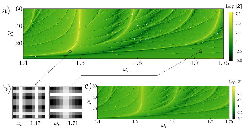
The erratic, random-like behavior of the impedance across our circuit suggests a hidden layer of emergent complexity in its resonance properties. Usually, one would expect a simple array of components to behave as a waveguide with resonances that are simple enough to list down, for instance like the vibration modes on a stretched drumskin [87, 88]. A complete impedance plot of our circuit in parameter space, however, reveals a complicated fractal-like structure that bears resemblance to the energy bands in the Hofstadter butterfly [89, 90, 91, 92]. In Fig. 3a, we observe the following intricate hierarchy of impedance peaks: apart from some “main” branches, there exists a proliferation of less regular peaks that appear and disappear with the discreteness of , akin to the cringes on the surface of a human palm. Additionally, these fractal patterns in our 2D circuit are not confined to 2D instances, much like the Hofstadter butterfly, which is specific to 3D and quasi-1D systems [93, 94].
To mathematically understand the origin of this fractal impedance behavior, we start from the formal expression for the impedance between two nodes and [61, 46]
| (2) |
where and are respectively the voltage potentials at the current input sites and at which is nonzero. Here and are the corresponding eigenvectors and eigenvalues of the Laplacian, whose pseudoinverse is given by , where indicates the omission of the uniform eigenvector corresponding to an overall voltage offset.
Evidently, impedance peaks arise if there are eigenvalues that are almost zero (not exactly zero, as they cannot perfectly vanish in a realistic circuit experiment). Such peaks have been featured as “topolectrical” resonances when the circuit band topology enforces topological zero modes [57, 95, 96]. In our context, there is no topological mechanism, and we proceed by deriving a compact albeit slightly complicated expression for the impedance between the corner nodes and , as detailed in “‘Methods: Detailed derivation of the corner-to-corner impedance”. The idea is to first consider the circuit under a doubled system with periodic boundaries where in Eq. (2) now labels the momentum eigenmodes , , and next employ the method of images to enforce the vanishing of currents across the open boundaries. In doing so, we obtain the impedance
| (3) |
The denominator in Eq. (3) resolves the origin of incommensurability leading to fractal-like behavior. Analogous to the Harper equation describing a Landau level due to a magnetic field [97, 89, 98, 99], we find the relation
| (4) |
describing a circuit resonance. Here, plays the analogous role to the energy in the Hofstadter butterfly, and plays the role of the denominator defining a fractional flux. In our case, however, all rational fractions with denominator simultaneously contribute to the impedance, and a strong resonance occurs if there exist integers of the same parity that accurately satisfy Eq. (4).
This relation explicitly expresses the resonance strength in terms of the commensurability properties of and , even though the relation is hard to guess from intuitive reasoning. Unlike the Hofstadter butterfly problem, which is based on magnetic translation-symmetric Bloch states [89, 91], our circuit setup contains no such symmetries. While generic (or likewise ) circuits do possess resonances, their resonance properties dimensionally depend on the frequency scale , and in general do not depend systematically on the system size. In our case, it is the mirror symmetry about the boundaries that fortuitously restores sufficient symmetry to give rise to an explicit, and hence also measurable, commensurability relation.
Stemming from the approximate solutions to Eq. (4), the impedance peaks are primarily manifestations of commensurate “energetics” that lead to a vanishing , rather than special spatial mode configurations. To illustrate this point, illustrative near-resonant and off-resonant eigenmodes of are plotted in Fig. 3b. Note that the near-resonant eigenmodes do not exhibit any spatial distribution particularities that distinguish them from ordinary eigenmodes contributing to far lower impedances.
II.4 Robustness of fractal impedance peaks and crossover from logarithmic scaling
In actual experiments, contact and parasitic resistances introduce inevitable dissipation and attenuate the impedance peaks, as evident in the comparison between Figs. 2c and 2d. Yet, the key anomalous fractal scaling behavior of the impedance remains robust. Phenomenologically, we can represent these dissipative effects through modifying the capacitor and inductor impedances to and , where and are real effective resistances. Incorporating the estimated and values from our experiments, which add an imaginary part of order to , we find that the fractal parameter space profile of the impedance becomes slightly smoothed out (Fig. 3c), even though the main branches of the fractal structure remains qualitatively unchanged. This robustness stems from the strong impedance divergence due to commensurability effects on a discretized conducting medium, which holds for generic lattice discretizations, and not just for our square lattice (Eq. (3)).
II.5 Anomalous impedance in the 2D honeycomb lattice
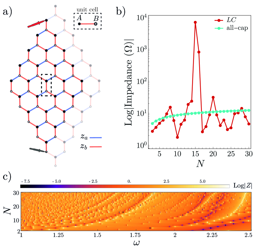
The presence of anomalous impedance in circuits is a universal property that arises when two distinct components with opposing phases are present in the circuit lattice. Here, we investigate the impedance characteristics of the two most distant nodes in a honeycomb lattice with a zigzag edge design. We consider nodes belonging to two sub-lattices and that are connected by an admittance (blue lines in Fig. 4a). The nearest neighbor nodes are also connected by an admittance (red lines in Fig. 4a) in a unit cell. The resultant lattice is fully reactive and non-resonant when and have the same phases and resonant when they have opposite phase. To investigate the lattice size-dependent impedance characteristics, we examine the circuit in both cases and find that there are anomalous impedance resonances at specific circuit sizes when the circuit parameters are fixed. Fig. 4b illustrates the impedance across circuit size behavior under two conditions: when the entire circuit is composed of only a single type of capacitor with a capacitance of , and when it is composed of two distinct admittances of and . The fractal scaling observed in the 2D circuit (Fig. 2a) also arises in the 2D honeycomb lattice. Fig. 4c illustrates the impedance resonances exhibiting fractal-like scaling with the variation of the circuit size and driving frequency. Furthermore, the edge design of the lattice affects only the form of the fractal-like branches, but the branches persist across different edge designs. This validates the fractal-like anomalous impedance scaling in circuits with different lattice models.
III Discussion
In this work, we theoretically and experimentally investigated the pronounced yet seemingly random impedance scaling behavior of circuit lattices arrays. This anomalous impedance scaling contrasts greatly with the usual logarithmic scaling expected in 2 dimensions, and is rooted in the commensurability properties of the circuit Green’s function eigenvalues, reminiscent of the commensurability conditions pertaining to a Hofstadter lattice with magnetic flux. This results in a curious fractal-like impedance behavior in the parameter space of dimensionless frequency and lattice size , whose complexity and structure elude any simplistic waveguide analysis.
In generic circuit lattices with more complex connections, unit cells, and feedback elements, more sophisticated fractal impedance fringes would be expected due to the more complicated commensurability conditions for the vanishing of the circuit Laplacian eigenvalues. This points towards the hitherto unnoticed general breakdown of a continuum description of resonant conducting media, which highlights the need for more careful analysis in the discretization of device geometries in electrostatics simulations. The discretization of continuous media involves dividing the medium into discrete units or elements that can be represented using discrete variables. In the context of electrical circuits, this can involve dividing continuous electrical fields or currents into discrete components such as resistors, capacitors, and inductors, which can be connected in various ways to create a circuit. Discretization allows for the use of mathematical tools and techniques to analyze physical phenomenon in an continuum media [100, 20], as in this study.
More generally, the fractal anomalous scaling behavior extends to the steady state behavior of systems governed by network Laplacians where a resonance frequency also enters the dynamics. This includes, for instance, directed information networks, which are physically unrelated to electrical circuits. While we have focused on a very regular square lattice network that should have possessed simple logarithmic impedance scaling naively, such fractal scaling also exists in more generic network structures, albeit in possibly more concealed manners.
IV Methods
IV.1 Detailed derivation of the corner-to-corner impedance
Here, we provide a detailed pedagogical exposition of the impedance formula in Eq. (3), which has an analytic expression thanks to the fact that the method of images can be used in implementing the circuit boundaries. Besides our method, one can also compute the complex equivalent resistance in finite complex lattices by using recursion-transform method [67, 68, 101].
The impedance is a measure of the total resistance that a circuit offers to the flow of alternating current. It is composed of reactance, which is the resistance of a circuit element to AC due to its inherent capacitance or inductance, and resistance, which is the resistance of a circuit element to AC due to its inherent properties (i.e., impedance , where and are the reactances corresponding to a capacitance and inductance , respectively, and is the resistance).
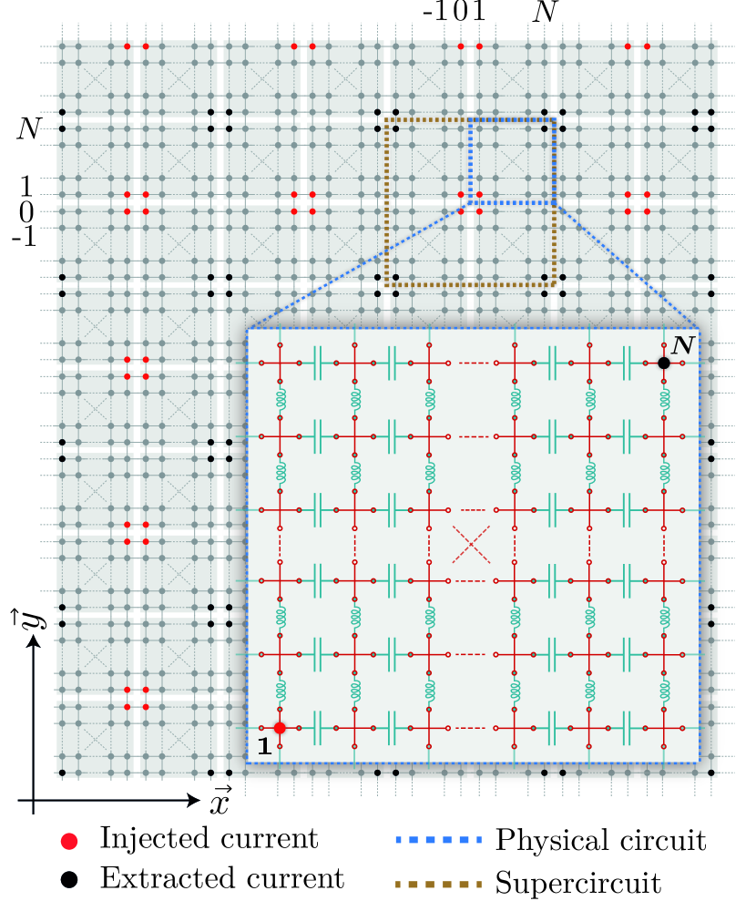
Any two-point impedance can be derived from Eq. (2), which requires determining the electric potential difference between two nodes in response to a current injected at node and extracted at node [61]. To derive the analytical corner-to-corner impedance expression for a finite square circuit, we consider an infinite circuit network built up from copies of the original circuit (see Fig. 5). (Here, is the circuit size in terms of the number of unit cells.) We then label the nodes in this infinite circuit lattice such that the diagonally opposite corner nodes of the physical single finite circuit are and , where , and and are the unit vectors for a 2-dimensional circuit. In such an infinite network, the current radiating from node r can be viewed in analogy to the flow of a current density through a material with conductivity in response to the electric field resulting in current distribution . Since where is the electric potential, we arrive at the Poisson’s equation
| (5) |
where in the continuum system is now replaced by , the coupling impedance between each neighbor in the circuit. To solve Eq. (5) for a single copy of the circuit array, we invoke the method of images, through which the electric potential in a specific region with boundaries can be obtained. In the context of electrostatics, a classic application of the method of images is to solve for the electric potential on a conducting plate stemming from a point charge. To achieve this, one can replace the conducting plate by an image charge of opposite sign located spatially opposite to the original charge [102, 103, 104, 105]. By using the same perspective, we can regard the finite circuit as the analog of the original source and its boundaries as conducting equipotential plates across which no current can flow [77]. Applying the method of images, the circuit is replicated to form a 2D infinite network with capacitive and inductive couplings along the horizontal and vertical links, respectively (refer Fig. 5). The Poisson equation in Eq. (5) is solved for this infinite 2D network. The solution for the node potentials within the boundaries of the source plate will correspond to the node potentials of the original finite circuit. This is because the presence of the replicas, which serve as the analogues of the image charges, ensures that the potential differences between all the edge nodes along the entire boundaries of the ‘source’ network and those of its image copies are zero. Hence, no current would flow across the edges of the source network, which is the exact boundary condition for the original finite circuit. To implement the method of images in the circuit network, we write the current distribution over the supercircuit with the period of as
| (6) |
where , . Here the vector for our 2D circuit is defined as where are integers varying between to and represents the Kronecker delta rather than the Dirac delta function of the continuum electrostatic model, due to the discrete locations of the injected/extracted currents (at the circuit nodes) and their finite magnitudes. Due to the inversion and translation symmetries of our circuit, the potential distribution produced by the current distribution can be obtained by translating the extracted currents by any multiple of the period, i.e., (see Fig. 5). Therefore, the voltage potential in Eq. (5) by means of the definition of the Green’s function and by considering all the image current injection/extraction points can be found as
| (7) | ||||
Now that we have reformulated the finite circuit problem as a problem on an infinite 2D lattice, we can find the momentum space Green’s function by employing the discrete Fourier transform (recalling ):
| (8) |
where is the corresponding circuit Laplacian given in Eq. (1). Here, the momentum space vectors for our 2D circuit are with and , where and are integer momentum indices from to . Because current is injected and extracted at opposite diagonal corners of the circuit and considering the translational invariance of the infinite circuit lattice, by symmetry [70, 106, 34], . Thus, . From the momentum space Green’s function of Eq. (8) and making use of Eq. (7),
| (9) | ||||
Here, the summation is taken over odd because in the numerator is zero when is even and when is odd. Notice that the unit impedance between the couplings in Eq. (7) is now replaced by the impedances and in the Laplacian in the denominator of Eq. (9). We convert the numerator of Eq. (9) to the trigonometric form by using the identity . After the transformation, the imaginary part of the expansion (i.e., the terms) disappears because it cancels out. The impedance between two opposite corners (i.e., node and node ) in our 2D circuit is then obtained as
| (10) |
where represents the two-point impedance between the two diagonally opposite nodes as a function of the circuit size and . The asterisk indicates that the summation should be taken only over odd values of where . Note that the summation can be performed over period due to the translation invariance. The condition for a vanishing denominator, i.e. divergent , is exactly that of the resonance condition given by Eq. (4).
IV.2 Determination of the fractal dimension
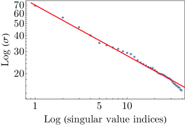
It is possible to estimate the fractal dimension by using the Singular Value Decomposition (SVD) method [107, 108, 109]. In this method, the self-similarities [110] or fractal dimension in a dataset, which is the fractal diagram in Fig. 3a (i.e., ), is given by one minus the slope of the log-log plot of the singular values of the fractal matrix [111, 112]. To determine the fractal dimension of our fractal structure, we performed SVD and write the decomposed matrices as
| (11) |
where (⊺) denotes the transpose operation, and are the left and right singular matrices, respectively, and is a diagonal matrix that comprises the singular values of the fractal. These diagonal values are nonnegative, and their squares give the eigenvalues of the matrix [108, 107]. We arrange the singular values in decreasing order, such that the largest value is , the second-largest is , and so on, i.e., . This allows us to determine the scaling ratio, which is defined as the ratio of the largest singular value to the fractal matrix dimension. For example, in our case in Fig. 3a, we find that and , and thus determine the scaling ratio as . The fractal dimension can be defined by utilizing the slope of the best linear fit in the log-log scale plot (Fig. 6) [113]. Therefore, the fractal dimension is determined as .
IV.3 Effects of inevitable parasitic resistances
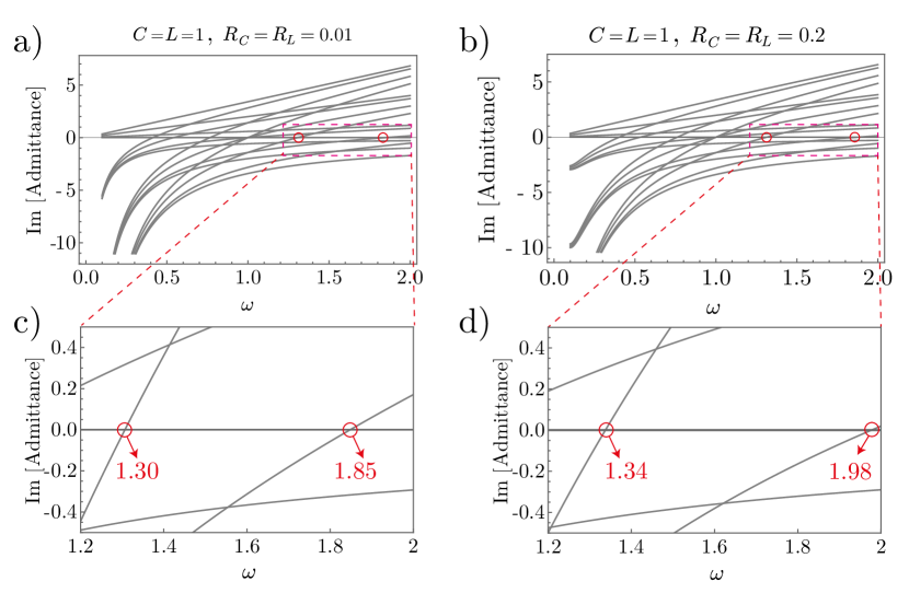
Theoretically, the parasitic resistances can be incorporated by introducing additional the real effective resistances for the capacitors and for the inductors, as we discussed in the main text. In Fig. 3c, we plot the fractal impedance peaks under the consideration of these parasitic resistances, which contribute to the imaginary part of the circuit resonance condition (). As can be seen in comparison with Fig. 3a, the realistic parasitic resistances only lead to a smooth shift of the impedance peak branches while the size-dependent resonances persist without further losses. This behavior can be understood from the admittance band structure. Since all the information for an ideal fully resonant media is contained within the imaginary part of its impedance, the presence of the parasitic resistances makes the impedance complex. This complexity implies that the stored energy represented by the imaginary part is dissipated due to the parasitic resistances. However, as long as the parasitic resistances do not become dominant, their presence results in a smooth shift in the frequency corresponding to zero admittance in the admittance band structure. To show this, we plot the admittance band structures in Fig. 7a, and 7b for our 2D circuit with by considering two different parasitic resistances. As evident from Figs. 7c and 7d, which provide a zoomed-in view of the band crossing points in panels (a) and (b) respectively, the admittance bands themselves remain qualitatively unchanged, although there is a shift towards higher frequencies in the admittance band structure. This is significant because impedance resonances occur in the presence of nearly zero eigenvalues, which correspond to the band-crossing points in the Laplacian formalism. According to Eq. (2), a large impedance is obtained when at least one of eigenvalues () becomes nearly zero provided that the wavefunction values at the measurement points of its corresponding eigenstate are not zero. Fig. 7 demonstrates that introducing small parasitic resistances results in a shift in the frequencies corresponding to the zero-energy eigenvalues. This explains the shift to the right in Fig. 3c and demonstrates the robustness of our circuit against parasitic resistances despite the smooth shift in the resonant frequencies.
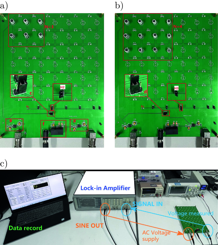
IV.4 Details of the experiment
Our experiment consists of measuring the corner-to-corner impedance of a square lattice array of elements, as pictured in Fig. 2a, b. To fit our measured impedances with the theoretical predictions, we introduce serial resistances to the and components, such that the effective becomes complex. Below, we detail the procedures involved, as well as some of the subtleties.
IV.4.1 Measurement process
Our measurements were performed on circuit lattices of different sizes corresponding to to (refer to Fig. 8a and 8b). To mitigate the effects of component disorder, the larger lattices were built by extending the smaller lattices, i.e., measurements are carried out on a circuit of size before the circuit was extended by soldering additional circuit elements to form a circuit of size .
Based on the fractal parameter space diagram, two AC frequency ranges of interest were determined as 115-175 kHz and 215-290 kHz. For each lattice size , we swept through both of these ranges with a sweep step size 200 Hz (an overly small step size will significantly increase the measurement time). The sweep time interval was set to 1000 ms, which was sufficient to ensure that the voltage reached a stable state each time the frequency was updated. For each point, the last three (stabilized) voltages were averaged and recorded. The configuration of the measurement setup is shown in Fig. 8c.
IV.4.2 Analysis of uncertainties
There are two main types of discrepancies between the theoretically predicted (Eq. (3)) and experimentally measured impedances. The first is the discrepancy between the predicted and measured resonant frequencies f0 where the impedance peaks, and the second is the discrepancy between the predicted and measured impedance values at f0. The first discrepancy can mainly be attributed to the uncertainties in the component values. The components we used are rated at , . Employing the frequency scale as a value estimator, we find that the discrepancy of f0 presented in Fig. 9 is within a reasonable range, as further tabulated in Table 1.
| Sim. with C=4.7nF 1%, L=1mH 5% | Sim. with C=4.7nF, L=1mH | Exp. | Error | |||||
|---|---|---|---|---|---|---|---|---|
| range of | range of | |||||||
| 3 | 123.4131.0 | 3.94.2 | 127.0 | 4.06 | 130.2 | 4.01 | 2.52% | -1.23% |
| 4 | 131.7139.8 | 7.68.2 | 135.6 | 7.96 | 139.4 | 7.59 | 2.80% | -4.65% |
| 5 | 135.5144.0 | 9.910.7 | 139.6 | 10.32 | 144.0 | 9.31 | 3.15% | -9.79% |
| 6 | 236.8251.4 | 1.81.9 | 243.8 | 1.86 | 250.4 | 1.95 | 2.71% | 4.84% |
| 7 | 248.9264.2 | 2.42.6 | 256.3 | 2.48 | 263.8 | 2.62 | 2.93% | 5.65% |
The second type of discrepancy, i.e., the impedance peak heights, is greatly affected by the parasitic resistance in addition to the component uncertainties. The parasitic resistance effectively suppress the peak of the measured impedance. This is reflected in the impedance-frequency curve in which the decrease in the peak value is accompanied by an increase in the FWHM (full width at half maximum), which makes it difficult to distinguish between the curves of different system sizes if the parasitic resistances were too large (fortunately, they were not). There may be several sources that contribute to parasitic effects, such as parasitic resistance, capacitance, and inductance. However, through numerous simulation studies, we found that the parasitic resistances are the most significant contributors that affect the measured impedance resonances. Using the estimated serial parasitic resistances of , , for the inductors, capacitors, and solder contacts respectively, we find that the experimental and simulation results match reasonably, as shown in Tables 1 and 2, and plotted in Fig. 2d of the main text.
IV.4.3 Reducing the influence of parasitic resistances
Parasitic resistance has a strong impact on the experiment. The most direct way to reduce its impact is to increase the inductances while decreasing the capacitances , since doing so does not necessitate a proportional increase in the parasitic resistances. However, the inductance value should not be too large in order to keep RpL within a reasonable range. At the same time, if the capacitance value is too small, the equivalent series resistance of the capacitors becomes dominant and the frequency increases, which may increase the uncertainty in the measurement. In order to strike a balance, we chose C=4.7 nF, L=1 mH.
IV.5 Determination of for experimental setups
Here, we provide details on how resistive contributions from and components (not necessarily parasitic) affect , which is the most important dimensionless parameter in our setup. The addition of serial resistances to each capacitor and inductor modifies their admittance contributions to the circuit Laplacian as follows:
| (12) | ||||
| (13) |
The Laplacian from the Eq. 1 of the main text is hence modified to
| (14) |
with the important parameter modified to
| (15) |
Substituting the measured parasitic resistances for our fabricated circuits via , and into the simulations, we find an excellent fit to the measured circuit impedances and their peaks (Fig. 2d of the main text). Their corresponding are given in Table 2. Note that an imaginary part of to was acquired due to these resistances. Since the components used were not of particularly high quality, can potentially be reduced by one or more orders if necessary - in our case, they already suffice for demonstrating the anomalous impedance scaling.
| Z max at N= | sim. | exp. | ||||||
|---|---|---|---|---|---|---|---|---|
| 3 | 127.0 | 130.2 | ||||||
| 4 | 135.6 | 139.4 | ||||||
| 5 | 139.6 | 144.0 | ||||||
| 6 | 243.8 | 250.4 | ||||||
| 7 | 256.3 | 263.8 | ||||||
IV.6 Data availability
All data can be acquired from the corresponding authors upon a reasonable request.
IV.7 Code availability
All code can be requested from the corresponding authors upon a reasonable request.
V References
References
- Fisher [1967] M. E. Fisher, The theory of equilibrium critical phenomena, Reports on Progress in Physics 30, 615 (1967).
- Stanley [1999] H. E. Stanley, Scaling, universality, and renormalization: Three pillars of modern critical phenomena, Reviews of Modern Physics 71, S358 (1999).
- Hilfer [1992] R. Hilfer, Scaling theory and the classification of phase transitions, Modern Physics Letters B 06, 773 (1992), publisher: World Scientific Publishing Co.
- Cardy [1996] J. Cardy, Scaling and Renormalization in Statistical Physics, Cambridge Lecture Notes in Physics (Cambridge University Press, Cambridge, 1996).
- Fröhlich [1983] J. Fröhlich, Scaling and Self-Similarity in Physics: Renormalization in Statistical Mechanics and Dynamics (Birkhäuser Boston, 1983).
- Chen [2016] W. Chen, Scaling theory of topological phase transitions, Journal of Physics: Condensed Matter 28, 055601 (2016), publisher: IOP Publishing.
- Zuo et al. [2021] Z. Zuo, S. Yin, X. Cao, and F. Zhong, Scaling theory of the Kosterlitz-Thouless phase transition, Physical Review B 104, 214108 (2021), publisher: American Physical Society.
- Leigh and Strassler [1995] R. G. Leigh and M. J. Strassler, Exactly marginal operators and duality in four dimensional n = 1 supersymmetric gauge theory, Nuclear Physics B 447, 95 (1995).
- Müller and Wyart [2015] M. Müller and M. Wyart, Marginal Stability in Structural, Spin, and Electron Glasses, Annual Review of Condensed Matter Physics 6, 177 (2015).
- Dresselhaus et al. [2021] E. J. Dresselhaus, B. Sbierski, and I. A. Gruzberg, Numerical evidence for marginal scaling at the integer quantum Hall transition, Annals of Physics Special Issue on Localisation 2020, 435, 168676 (2021).
- Zirnbauer [2021] M. R. Zirnbauer, Marginal CFT perturbations at the integer quantum Hall transition, Annals of Physics 431, 168559 (2021).
- MacKinnon and Kramer [1983] A. MacKinnon and B. Kramer, The scaling theory of electrons in disordered solids: Additional numerical results, Zeitschrift für Physik B Condensed Matter 53, 1 (1983).
- Poland et al. [2019] D. Poland, S. Rychkov, and A. Vichi, The conformal bootstrap: Theory, numerical techniques, and applications, Reviews of Modern Physics 91, 015002 (2019).
- Zamolodchikov [1989] A. B. Zamolodchikov, Exact solutions of conformal field theory in two dimensions and critical phenomena, Reviews in Mathematical Physics 01, 197 (1989).
- Lee and Ramakrishnan [1985] P. A. Lee and T. V. Ramakrishnan, Disordered electronic systems, Reviews of Modern Physics 57, 287 (1985).
- Albert and Barabási [2002] R. Albert and A.-L. Barabási, Statistical mechanics of complex networks, Reviews of Modern Physics 74, 47 (2002), publisher: American Physical Society.
- Chen et al. [2021] H.-X. Chen, M.-Y. Wang, W.-J. Chen, X.-Y. Fang, and Z.-Z. Tan, Equivalent complex impedance of n-order RLC network, Phys. Scr. 96, 075202 (2021).
- Tan et al. [2019] Z. Tan, Z.-Z. Tan, J. H. Asad, and M. Q. Owaidat, Electrical characteristics of the 2 n and n circuit network, Phys. Scr. 94, 055203 (2019).
- Bartis [1967] F. J. Bartis, Let’s Analyze the Resistance Lattice, American Journal of Physics 35, 354 (1967).
- Kirkpatrick [1973] S. Kirkpatrick, Percolation and Conduction, Rev. Mod. Phys. 45, 574 (1973).
- Venezian [1994] G. Venezian, On the resistance between two points on a grid, American Journal of Physics 62, 1000 (1994).
- Lavatelli [1972] L. Lavatelli, The Resistive Net and Finite-Difference Equations, American Journal of Physics 40, 1246 (1972).
- Zemanian [1984] A. H. Zemanian, A classical puzzle: The driving-point resistances of infinite grids, IEEE Circuits Syst. Mag. 6, 7 (1984).
- Aitchison [1964] R. E. Aitchison, Resistance between Adjacent Points of Liebman Mesh, American Journal of Physics 32, 566 (1964).
- Montroll and Weiss [1965] E. W. Montroll and G. H. Weiss, Random Walks on Lattices. II, Journal of Mathematical Physics 6, 167 (1965).
- Morita [1971] T. Morita, Useful Procedure for Computing the Lattice Green’s Function‐Square, Tetragonal, and bcc Lattices, Journal of Mathematical Physics 12, 1744 (1971).
- Asad et al. [2014] J. Asad, A. Diab, M. Owaidat, and J. Khalifeh, Perturbed Infinite 3D Simple Cubic Network of Identical Capacitors, Acta Phys. Pol. A 126, 777 (2014).
- Owaidat et al. [2016] M. Q. Owaidat, J. H. Asad, and Z.-Z. Tan, On the perturbation of a uniform tiling with resistors, Int. J. Mod. Phys. B 30, 1650166 (2016).
- Giordano [2005] S. Giordano, Disordered lattice networks: general theory and simulations, Int. J. Circ. Theor. Appl. 33, 519 (2005).
- Cserti et al. [2002] J. Cserti, G. Dávid, and A. Piróth, Perturbation of infinite networks of resistors, American Journal of Physics 70, 153 (2002).
- Lee [2021] C. H. Lee, Many-body topological and skin states without open boundaries, Phys. Rev. B 104, 195102 (2021).
- Izmailian and Kenna [2014] N. S. Izmailian and R. Kenna, A generalised formulation of the Laplacian approach to resistor networks, J. Stat. Mech. 2014, P09016 (2014).
- Tan et al. [2017a] Z.-Z. Tan, J. Asad, and M. Owaidat, Resistance formulae of a multipurpose n -step network and its application in LC network: Resistance Formulae of a Multipurpose n -Step Network, Int. J. Circ. Theor. Appl. 45, 1942 (2017a).
- Cserti et al. [2011] J. Cserti, G. Széchenyi, and G. Dávid, Uniform tiling with electrical resistors, J. Phys. A: Math. Theor. 44, 215201 (2011).
- Owaidat et al. [2010] M. Q. Owaidat, R. S. Hijjawi, and J. M. Khalifeh, Interstitial single resistor in a network of resistors application of the lattice Green’s function, J. Phys. A: Math. Theor. 43, 375204 (2010).
- Asad et al. [2005] J. H. Asad, R. S. Hijjawi, A. J. Sakaji, and J. M. Khalifeh, Infinite network of identical capacitors by green’s function, Int. J. Mod. Phys. B 19, 3713 (2005).
- Doyle and Snell [1984] P. G. Doyle and J. L. Snell, Random walks and electric networks, Vol. 22 (American Mathematical Soc., 1984).
- Mamode [2019] M. Mamode, Calculation of two-point resistances for conducting media needs regularization of Coulomb singularities, Eur. Phys. J. Plus 134, 559 (2019).
- Pan et al. [2021] N. Pan, T. Chen, H. Sun, and X. Zhang, Electric-Circuit Realization of Fast Quantum Search, Research 2021, 1 (2021).
- Chen et al. [2019] H.-X. Chen, L. Yang, and M.-J. Wang, Electrical characteristics of n-ladder network with internal load, Results in Physics 15, 102488 (2019).
- Chen and Tan [2020a] C.-P. Chen and Z.-Z. Tan, Electrical characteristics of an asymmetric N-step network, Results in Physics 19, 103399 (2020a).
- Chen et al. [2020] H.-X. Chen, N. Li, Z.-T. Li, and Z.-Z. Tan, Electrical characteristics of a class of n-order triangular network, Physica A: Statistical Mechanics and its Applications 540, 123167 (2020).
- Chen and Tan [2020b] H.-X. Chen and Z.-Z. Tan, Electrical properties of an n -order network with Y circuits, Phys. Scr. 95, 085204 (2020b).
- Chen and Yang [2020] H.-X. Chen and L. Yang, Electrical characteristics of n-ladder network with external load, Indian J Phys 94, 801 (2020).
- Ammar et al. [2022] N. Ammar, J. Asad, and R. Jarrar, Electrical characteristics for triangular resistors–capacitors–inductors network designed on two coats, Circuit Theory & Apps 50, 153 (2022).
- Lee et al. [2018] C. H. Lee, S. Imhof, C. Berger, F. Bayer, J. Brehm, L. W. Molenkamp, T. Kiessling, and R. Thomale, Topolectrical Circuits, Communications Physics 1, 1 (2018).
- Li et al. [2019] L. Li, C. H. Lee, and J. Gong, Emergence and full 3d-imaging of nodal boundary seifert surfaces in 4d topological matter, Communications physics 2, 135 (2019).
- Wang et al. [2020] Y. Wang, H. M. Price, B. Zhang, and Y. D. Chong, Circuit implementation of a four-dimensional topological insulator, Nat Commun 11, 2356 (2020).
- Wang et al. [2022] H. Wang, W. Zhang, H. Sun, and X. Zhang, Observation of inverse anderson transitions in aharonov-bohm topolectrical circuits, Phys. Rev. B 106, 104203 (2022).
- Shang et al. [2022] C. Shang, S. Liu, R. Shao, P. Han, X. Zang, X. Zhang, K. N. Salama, W. Gao, C. H. Lee, R. Thomale, A. Manchon, S. Zhang, T. J. Cui, and U. Schwingenschlögl, Experimental Identification of the Second‐Order Non‐Hermitian Skin Effect with Physics‐Graph‐Informed Machine Learning, Advanced Science 9, 2202922 (2022).
- Wu et al. [2023] M. Wu, Q. Zhao, L. Kang, M. Weng, Z. Chi, R. Peng, J. Liu, D. H. Werner, Y. Meng, and J. Zhou, Evidencing non-bloch dynamics in temporal topolectrical circuits, Phys. Rev. B 107, 064307 (2023).
- Zhang et al. [2023] H. Zhang, T. Chen, L. Li, C. H. Lee, and X. Zhang, Electrical circuit realization of topological switching for the non-hermitian skin effect, Phys. Rev. B 107, 085426 (2023).
- Hohmann et al. [2023] H. Hohmann, T. Hofmann, T. Helbig, S. Imhof, H. Brand, L. K. Upreti, A. Stegmaier, A. Fritzsche, T. Müller, U. Schwingenschlögl, C. H. Lee, M. Greiter, L. W. Molenkamp, T. Kießling, and R. Thomale, Observation of cnoidal wave localization in nonlinear topolectric circuits, Phys. Rev. Res. 5, L012041 (2023).
- Tuloup et al. [2020] T. Tuloup, R. W. Bomantara, C. H. Lee, and J. Gong, Nonlinearity induced topological physics in momentum space and real space, Phys. Rev. B 102, 115411 (2020).
- Kotwal et al. [2021] T. Kotwal, F. Moseley, A. Stegmaier, S. Imhof, H. Brand, T. Kießling, R. Thomale, H. Ronellenfitsch, and J. Dunkel, Active topolectrical circuits, Proc. Natl. Acad. Sci. U.S.A. 118, e2106411118 (2021).
- Kengne et al. [2022] E. Kengne, W.-M. Liu, L. Q. English, and B. A. Malomed, Ginzburg–Landau models of nonlinear electric transmission networks, Physics Reports 982, 1 (2022).
- Ningyuan et al. [2015] J. Ningyuan, C. Owens, A. Sommer, D. Schuster, and J. Simon, Time- and site-resolved dynamics in a topological circuit, Phys. Rev. X 5, 021031 (2015).
- Rafi-Ul-Islam et al. [2020] S. M. Rafi-Ul-Islam, Z. Bin Siu, and M. B. A. Jalil, Topoelectrical circuit realization of a Weyl semimetal heterojunction, Commun Phys 3, 72 (2020).
- Kapitanova et al. [2014] P. V. Kapitanova, P. Ginzburg, F. J. Rodríguez-Fortuño, D. S. Filonov, P. M. Voroshilov, P. A. Belov, A. N. Poddubny, Y. S. Kivshar, G. A. Wurtz, and A. V. Zayats, Photonic spin Hall effect in hyperbolic metamaterials for polarization-controlled routing of subwavelength modes, Nat Commun 5, 3226 (2014).
- Wu [2004] F. Y. Wu, Theory of resistor networks: the two-point resistance, J. Phys. A: Math. Gen. 37, 6653 (2004).
- Tzeng and Wu [2006] W. J. Tzeng and F. Y. Wu, Theory of impedance networks: the two-point impedance and LC resonances, J. Phys. A: Math. Gen. 39, 8579 (2006).
- Čerňanová et al. [2014] V. Čerňanová, J. Brenkuŝ, and V. Stopjaková, Non–Symmetric Finite Networks: The Two–Point Resistance, Journal of Electrical Engineering 65, 283 (2014).
- Tan [2016] Z.-Z. Tan, Two-point resistance of an m × n resistor network with an arbitrary boundary and its application in RLC network, Chinese Phys. B 25, 050504 (2016).
- Tan et al. [2017b] Z.-z. Tan, H. Zhu, J. H. Asad, C. Xu, and H. Tang, Characteristic of the equivalent impedance for an m×n RLC network with an arbitrary boundary, Frontiers Inf Technol Electronic Eng 18, 2070 (2017b).
- Fang and Tan [2022] X.-Y. Fang and Z.-Z. Tan, Circuit network theory of n-horizontal bridge structure, Sci Rep 12, 6158 (2022).
- Zhou et al. [2017] L. Zhou, Z.-z. Tan, and Q.-h. Zhang, A fractional-order multifunctional n-step honeycomb RLC circuit network, Frontiers Inf Technol Electronic Eng 18, 1186 (2017).
- Tan [2015a] Z.-Z. Tan, Recursion-transform method for computing resistance of the complex resistor network with three arbitrary boundaries, Phys. Rev. E 91, 052122 (2015a).
- Tan [2015b] Z.-Z. Tan, Recursion-transform approach to compute the resistance of a resistor network with an arbitrary boundary, Chinese Phys. B 24, 020503 (2015b).
- Joyce [2017] G. S. Joyce, Exact results for the diamond lattice Green function with applications to uniform random walks in a plane, J. Phys. A: Math. Theor. 50, 425001 (2017).
- [70] J. Cserti, Application of the lattice green’s function for calculating the resistance of an infinite network of resistors, American Journal of Physics 68, 896.
- Katsura et al. [1971] S. Katsura, T. Morita, S. Inawashiro, T. Horiguchi, and Y. Abe, Lattice Green’s Function. Introduction, Journal of Mathematical Physics 12, 892 (1971).
- Mamode [2021] M. Mamode, Revisiting the discrete planar Laplacian: exact results for the lattice Green function and continuum limit, Eur. Phys. J. Plus 136, 412 (2021).
- Joyce [2002] G. S. Joyce, Exact evaluation of the simple cubic lattice Green function for a general lattice point, J. Phys. A: Math. Gen. 35, 9811 (2002).
- G.S [1973] J. G.S, On the simple cubic lattice Green function, Philosophical Transactions of the Royal Society of London. Series A, Mathematical and Physical Sciences 273, 32 (1973).
- Essam and Wu [2009] J. W. Essam and F. Y. Wu, The exact evaluation of the corner-to-corner resistance of an M × N resistor network: asymptotic expansion, J. Phys. A: Math. Theor. 42, 025205 (2009).
- Izmailian and Huang [2010] N. S. Izmailian and M.-C. Huang, Asymptotic expansion for the resistance between two maximally separated nodes on an M by N resistor network, Phys. Rev. E 82, 011125 (2010).
- [77] M. Mamode, Electrical resistance between pairs of vertices of a conducting cube and continuum limit for a cubic resistor network, Journal of Physics Communications 1, 035002.
- Sahin et al. [2023] H. Sahin, Z. B. Siu, S. M. Rafi-Ul-Islam, J. F. Kong, M. B. A. Jalil, and C. H. Lee, Impedance responses and size-dependent resonances in topolectrical circuits via the method of images, Phys. Rev. B 107, 245114 (2023).
- Callan [1970] C. G. Callan, Broken Scale Invariance in Scalar Field Theory, Physical Review D 2, 1541 (1970).
- Fisher [1974] M. E. Fisher, The renormalization group in the theory of critical behavior, Reviews of Modern Physics 46, 597 (1974).
- Wilson [1975] K. G. Wilson, The renormalization group: Critical phenomena and the Kondo problem, Reviews of Modern Physics 47, 773 (1975).
- Abrahams et al. [1979] E. Abrahams, P. W. Anderson, D. C. Licciardello, and T. V. Ramakrishnan, Scaling Theory of Localization: Absence of Quantum Diffusion in Two Dimensions, Physical Review Letters 42, 673 (1979).
- Altshuler et al. [1980] B. L. Altshuler, A. G. Aronov, and P. A. Lee, Interaction Effects in Disordered Fermi Systems in Two Dimensions, Physical Review Letters 44, 1288 (1980).
- Abrahams et al. [1981] E. Abrahams, P. W. Anderson, P. A. Lee, and T. V. Ramakrishnan, Quasiparticle lifetime in disordered two-dimensional metals, Physical Review B 24, 6783 (1981).
- García-García and Wang [2005] A. M. García-García and J. Wang, Anderson Transition in Quantum Chaos, Phys. Rev. Lett. 94, 244102 (2005).
- García-García and Wang [2006] A. M. García-García and J. Wang, Semi-Poisson statistics in quantum chaos, Phys. Rev. E 73, 036210 (2006).
- Kac [1966] M. Kac, Can one hear the shape of a drum?, The American Mathematical Monthly 73, 1 (1966), https://doi.org/10.1080/00029890.1966.11970915 .
- Tien [1977] P. K. Tien, Integrated optics and new wave phenomena in optical waveguides, Rev. Mod. Phys. 49, 361 (1977).
- Hofstadter [1976] D. R. Hofstadter, Energy levels and wave functions of Bloch electrons in rational and irrational magnetic fields, Physical Review B 14, 2239 (1976).
- Albrecht et al. [2001] C. Albrecht, J. H. Smet, K. von Klitzing, D. Weiss, V. Umansky, and H. Schweizer, Evidence of Hofstadter’s Fractal Energy Spectrum in the Quantized Hall Conductance, Physical Review Letters 86, 147 (2001).
- Koshino and Ando [2006] M. Koshino and T. Ando, Hall plateau diagram for the Hofstadter butterfly energy spectrum, Phys. Rev. B 73, 155304 (2006).
- Hunt et al. [2013] B. Hunt, J. D. Sanchez-Yamagishi, A. F. Young, M. Yankowitz, B. J. LeRoy, K. Watanabe, T. Taniguchi, P. Moon, M. Koshino, P. Jarillo-Herrero, and R. C. Ashoori, Massive Dirac Fermions and Hofstadter Butterfly in a van der Waals Heterostructure, Science 340, 1427 (2013), https://www.science.org/doi/pdf/10.1126/science.1237240 .
- Koshino et al. [2001] M. Koshino, H. Aoki, K. Kuroki, S. Kagoshima, and T. Osada, Hofstadter Butterfly and Integer Quantum Hall Effect in Three Dimensions, Physical Review Letters 86, 1062 (2001).
- Koshino et al. [2002] M. Koshino, H. Aoki, T. Osada, K. Kuroki, and S. Kagoshima, Phase diagram for the Hofstadter butterfly and integer quantum Hall effect in three dimensions, Physical Review B 65, 045310 (2002).
- Imhof et al. [2018] S. Imhof, C. Berger, F. Bayer, J. Brehm, L. W. Molenkamp, T. Kiessling, F. Schindler, C. H. Lee, M. Greiter, T. Neupert, and R. Thomale, Topolectrical-circuit realization of topological corner modes, Nature Physics 14, 925 (2018).
- Yang et al. [2020] H. Yang, Z.-X. Li, Y. Liu, Y. Cao, and P. Yan, Observation of symmetry-protected zero modes in topolectrical circuits, Physical Review Research 2, 022028 (2020).
- Harper [1955] P. G. Harper, Single Band Motion of Conduction Electrons in a Uniform Magnetic Field, Proceedings of the Physical Society. Section A 68, 874 (1955).
- Krasovsky [1999] I. V. Krasovsky, Bethe ansatz for the Harper equation: Solution for a small commensurability parameter, Physical Review B 59, 322 (1999).
- Poshakinskiy et al. [2021] A. V. Poshakinskiy, J. Zhong, Y. Ke, N. A. Olekhno, C. Lee, Y. S. Kivshar, and A. N. Poddubny, Quantum Hall phases emerging from atom–photon interactions, npj Quantum Inf 7, 34 (2021).
- Webman et al. [1977] I. Webman, J. Jortner, and M. H. Cohen, Theory of optical and microwave properties of microscopically inhomogeneous materials, Phys. Rev. B 15, 5712 (1977).
- Tan [2017] Z.-Z. Tan, Recursion-transform method and potential formulae of the m × n cobweb and fan networks, Chinese Phys. B 26, 090503 (2017).
- [102] K. F. Riley, M. P. Hobson, and S. J. Bence, Mathematical methods for physics and engineering (American Association of Physics Teachers).
- [103] D. J. Griffiths, Introduction to electrodynamics (American Association of Physics Teachers).
- [104] J. D. Jackson, Classical electrodynamics (American Association of Physics Teachers).
- Yang et al. [2022] R. Yang, J. W. Tan, T. Tai, J. M. Koh, L. Li, S. Longhi, and C. H. Lee, Designing non-Hermitian real spectra through electrostatics, Science Bulletin 67, 1865 (2022).
- [106] D. Atkinson and F. J. van Steenwijk, Infinite resistive lattices, American Journal of Physics 67, 486.
- Weng et al. [2022] X. Weng, A. Perry, M. Maroun, and L. T. Vuong, Singular Value Decomposition and Entropy Dimension of Fractals, in 2022 International Conference on Image Processing, Computer Vision and Machine Learning (ICICML) (IEEE, Xi’an, China, 2022) pp. 427–431.
- Alter et al. [2000] O. Alter, P. O. Brown, and D. Botstein, Singular value decomposition for genome-wide expression data processing and modeling, Proc. Natl. Acad. Sci. U.S.A. 97, 10101 (2000).
- Lee et al. [2015] C. H. Lee, Y. Yamada, T. Kumamoto, and H. Matsueda, Exact Mapping from Singular-Value Spectrum of Fractal Images to Entanglement Spectrum of One-Dimensional Quantum Systems, J. Phys. Soc. Jpn. 84, 013001 (2015).
- Mishra and Barman [2021] R. C. Mishra and H. Barman, Effective resistances of two-dimensional resistor networks, Eur. J. Phys. 42, 015205 (2021).
- Malcai et al. [1997] O. Malcai, D. A. Lidar, O. Biham, and D. Avnir, Scaling range and cutoffs in empirical fractals, Phys. Rev. E 56, 2817 (1997).
- Carr and Benzer [1991] J. R. Carr and W. B. Benzer, On the practice of estimating fractal dimension, Math Geol 23, 945 (1991).
- Faloutsos et al. [2021] C. Faloutsos, L. Wu, A. Traina, and C. Traina Jr., Fast feature selection using fractal dimension, Journal of Information and Data Management 1, 3 (2021).
VI Acknowledgments
This work was supported by the Ministry of Education (MOE) of Singapore Tier-II (Grant Nos. MOE2018-T2-2-117 and MOET2EP50121-0014) and MOE Tier-I FRC (Grant Nos. A-0005110-01-00 and A-8000195-01-00). CHL acknowledges support from Singapore Ministry of Education’s Tier I grant A-8000022-00-00. HS would like to thank the Agency for Science, Technology and Research (A*STAR) for its support of our research through the SINGA fellowship program.
VI.1 Author contributions
C.H.L. initiated the idea, proposed the first draft of the manuscript, and supervised the entire project. H.S. conducted preliminary studies, performed theoretical calculations, and contributed to parts of the writing. Z.B.S. assisted in improving the theoretical analysis and formulations. X.Z. and B.Z. designed and executed the experiment, analyzed the data, and wrote the experimental details. S.M.R., J.F.K., B.S., R.T., and M.B.J. reviewed and contributed to all aspects of the manuscript.
VI.2 Competing interests
The authors declare no competing interests.