Hybrid photonic-plasmonic cavity design for very large Purcell factors at telecom wavelengths
Abstract
Hybrid photonic-plasmonic cavities can be tailored to display high -factors and extremely small mode volumes simultaneously, which results in large values of the Purcell factor, . Amongst the different hybrid configurations, those based on a nanoparticle-on-a-mirror (NPoM) plasmonic cavity provide one of the lowest mode volumes, though so far their operation has been constrained to wavelengths below 1 m. Here, we propose a hybrid configuration consisting of a silicon photonic crystal cavity with a slot at its center in which a gold nanoparticle is introduced. This hybrid system operates at telecom wavelengths and provides high -factor values () and small normalized mode volumes (), leading to extremely large Purcell factor values, . The proposed cavity could be used in different applications such as molecular optomechanics, bio- and chemo-sensing, all-optical signal processing or enhanced Raman spectroscopy in the relevant telecom wavelength regime.
I Introduction \\
The local density of optical states (LDOS) quantifies the available amount of electromagnetic states that can be occupied by a photon in a certain position of a system. A high local value of the LDOS will result in enhanced light-matter interaction there. This way, the environment of an emitter can be tailored to maximize the LDOS, for instance, using optical cavities. At resonance, the LDOS gives us the Purcell factor, , which originally accounted for the enhancement of the spontaneous emission of an atom in a cavity [1, 2, 3]. By definition, the Purcell factor is proportional to the ratio between the -factor and the mode volume as [4, 5]:
| (1) |
where is the mode volume normalized by the wavelength () over the local refractive index () cubed , and is the quality factor. This suggests a route to design photonic systems that exhibit simultaneously high -factor and ultra small to maximize and enhance light-matter interaction.
Dielectric cavities can greatly enhance the Purcell factor since they can have high -factor values as a result of the negligible absorption loss [6]. However, the diffraction limit usually prevents them to achieve subwavelength-scale mode volumes, so unless special “slotted” configurations are used [7, 8, 9]. On the contrary, plasmonic cavities formed by metallic nanoparticles (NPs) can overcome the diffraction limit leading to ultrasmall values[10]. However, Joule’s losses in the metal reduces the reachable -factor to values [11, 12].
In the last few years, hybrid photonic-plasmonic cavities have been introduced as novel systems providing large as they can potentially combine the best of both worlds: high -factor values due to the dielectric photonic cavity and small mode volumes thanks to the metallic NP [11, 13, 14, 15, 16, 17, 18, 19, 20, 21, 22]. Indeed, by modifying the coupling between photonic and plasmonic modes, the -factor and can be tuned between the values of the bare NP and the cavity [17]. Different configurations of hybrid photonic-plasmonic cavities have been suggested so far. Some of the most attractive ones consist of a bow-tie nanoantenna placed on a dielectric photonic crystal nanobeam cavity operating at transverse-electric polarization [17] (). The main limitation of this configuration is that the plasmonic gap has to be defined lithographically reaching minimum values of several nm, which prevents reaching the nm-scale (and below) gaps that leads to extreme plasmonic localization [23, 24, 25].
Nanoparticle-on-a-mirror (NPoM) cavities are far superior to achieve the smallest possible mode volumes, as plasmonic gaps around 1 nm and below can be created. The reason is that NPs can be deposited on top of self-assembled monolayers (SAMs) formed on metallic surfaces so the plasmonic gap widths equal the SAM thickness [26, 27, 28, 29, 30]. Recently, a hybrid system combining a NPoM configuration with GaP photonic crystal cavities - operating under transverse-magnetic polarization at visible wavelengths - has been introduced [31]. Thanks to the NPoM-based design, nm- and sub-nm-scale plasmonic gaps potentially can be achieved and combined with relatively large -factors. By means of this novel hybrid system, the Purcell factor values are enhanced one order of magnitude with respect to the hybrid configurations based on bow-tie nanoantennas () [31].
Most of the previous works on hybrid photonic cavities have been focused on the visible wavelength range due to the huge interest in enhancing light-matter interaction in that band [17]. However, at the telecom wavelengths ( nm) is highly interesting. First, because of the multiple available applications (mostly related to high-speed optical communications and data processing) as well as advanced available equipment (laser, amplifiers and high-speed photodetectors); and, second, because of the emergence of the silicon photonics area, which has become the mainstream technology for photonic integrated circuits. Indeed, there have been many demonstrations of silicon cavities operating at telecom wavelengths with factors over using lithographically-defined 1D () [32] or 2D () [33] photonic crystal cavities whilst showing . Reaching becomes feasible by defining thin slots in silicon and taking advantage of the discontinuities of the normal electric field [34, 7], but with the minimum slot size imited by lithography. In previous work [8], complex subwavelength structuring of silicon (down to nm) enabled to get also .
Owing to this technological interest, hybrid systems have also been recently proposed in silicon technology for telecom wavelengths. In [19], a hybrid photonic-plasmonic nano-cavity, constituted by an L3 photonic crystal nano-cavity and a plasmonic bow-tie nanoantenna was shown to have an ultrahigh figure of merit of (). However, either in the only-silicon cavity [8], or in the hybrid approach [19] the extreme localization enabled by the NPoM is still missing.
In this work, we propose a hybrid photonic-plasmonic cavity that combines silicon and the NPoM configuration to get extreme field localization at resonance. This hybrid consists of a silicon photonic cavity with a slot at its center [34, 9], operating at transverse-electric polarization at telecom wavelengths, and a gold NP, which is located at the slot’s cavity. The NP can be potentially separated from the silicon walls of the slot by a SAM, thus reaching the nm- and even sub-nm-scale localized fields at resonance. Our design achieves and , giving rise to Purcell factor values of , which are two-three orders of magnitude larger than those reported previously based on NPoM cavities combined with photonic crystals and two orders of magnitude larger than those corresponding to hybrid photonic-plasmonic cavities operating at telecom wavelengths. This is mainly due to the nanoscale confinement provided by the slot-nanoparticle combination and the radiation suppression resulting from the photonic crystal structure.
We also suggest a route to fabricate - combining top-down and bottom-up approaches - the hybrid cavity, which may be used to improve the performance of current silicon photonic devices as well as to envisage new applications in the relevant telecom-wavelength domain.
II Hybrid system description
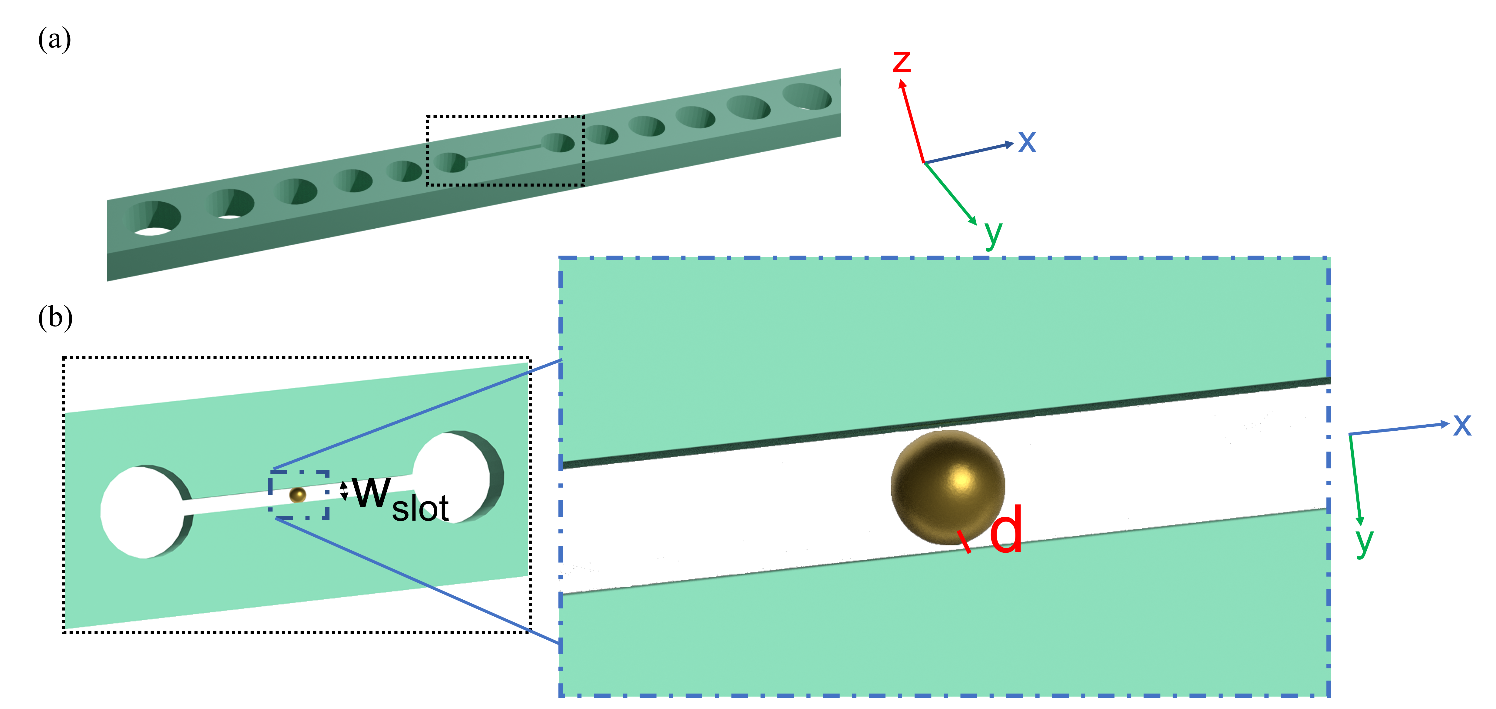
Figure 1 depicts the proposed hybrid photonic-plasmonic configuration. A gold NP is located at the center of the slot of a 1D silicon photonic crystal cavity operating under transverse-electric polarization at telecom wavelengths. The distance between the NP and the photonic crystal wall (gap, ) is nm, which approximately models the thickness of a SAM. The silicon wall behaves here as the mirror, though with lower reflectance than for a metallic one. Such a small gap, which is not defined lithographically but after depositing the NP after the silicon cavity is fabricated, should allow for extreme light confinement, thus giving rise to small . In addition, high -factors can be achieved due to the photonic bandgap of the dielectric cavity.
III Methods
The eigenfrequencies and LDOS calculations shown in this work were obtained by means of the Finite Element Method (FEM), implemented in the commercial software COMSOL Multiphysics [35]. In particular, the Radio Frequency (RF) Module was used. The optical constants for the gold NP were taken from Ref. [36]. The refractive index for silicon was considered as . To attain the LDOS, the structure was illuminated by an electric point-dipole source, whose dipole moment was considered along the -axis (i.e. along the axis connecting the sphere and the cavity). The normalized LDOS is defined as
| (2) |
where is the radiative power density and is the total power loss density. The numerator corresponds to the radiative and nonradiative power emitted by the dipole coupled to the structure. However, the denominator contains the radiative power emitted by the dipole in a vacuum. The dipole was located at the center of the structure and in the middle of the gap between the NP and the cavity. Experimentally, this spacer would be filled by a SAM. The hybrid geometry was surrounded by a cylindrical air region of radius 9 m. An additional smaller cylinder with a radius of 5 m and made of air was placed in the center of the larger cylinder. The scattered power () was calculated at the boundaries of the smaller cylinder, whereas the total power loss density was obtained by means of the volume integration of the losses in the metallic NP. The dipole source was surrounded by a sphere with a diameter that is equal to the gap size ( nm) to ensure a sufficient fine grid in close proximity to the dipole source. The mesh of the surrounding air medium was chosen to be smaller than 600 nm. The mesh of the gold sphere was smaller than 6 nm. The chosen sizes for the mesh of the slot, cavity surrounding the slot, holes and cavity surrounding the holes were smaller than 15 nm, 22.5 nm, 45 nm and 52.5 nm, respectively. The mesh of the sphere surrounding the dipole source was smaller than 0.2 nm. The cylindrical region of air was surrounded by a perfectly matched layer (PML) with a thickness of 3 m.
The near-field plots at the eigenfrequencies of interest were attained with the eigenmode solver of COMSOL Multiphysics. The same mesh was used for the LDOS and eigenmode calculations and for the different analyzed structures: dielectric (no NP) and hybrid cavity. In all the cases, the same geometry was considered, and only optical constants of the materials (if present or not) were changed appropriately.
IV Results
IV.1 Photonic band diagram
The 1D silicon photonic crystal cavity consists of a silicon waveguide of width nm and thickness nm patterned with holes and with a slot in the defect section, as depicted in Figure 1(a). The beam is drilled by a set of circular holes to produce a transverse-electric (TE) band gap around nm. Figure 2(a) shows the TE-like band diagram when the holes are spaced by a distance nm and have a radius , showing a wide bandgap (shadowed region) as expected. To build the cavity, we include two photonic crystal mirrors with the previous dimensions at each side of the cavity whilst the period is adiabatically reduced from nm down to nm (keeping constant the ratio) when moving to the cavity center. This permits to blue-shift the dielectric band and get a confined mode in the band gap, as depicted by the red dashed line in Fig. 2(a). Finally, a slot section of width nm and length nm is introduced between the central holes of the cavity to enhanced the transverse electric field. Notice that this slot width is achievable using standard silicon nanofabrication [9].
Figure 2(b) represents the near-field map at the eigenfrequency of the confined mode ( nm) in the 1D photonic crystal cavity following the previous design. It can be clearly seen that the electric field is well confined in the slot placed at the center of the cavity. It is worth mentioning that the cavity resonance is red-shifted with respect to the gold NP resonance. In previous works, it was evidenced that this condition is necessary to improve the performance of the hybrid cavity with respect to the bare components [17, 11, 18].
IV.2 Comparison - values for the bare cavity and hybrid system
In Figs. 3(a) and (b), we represent the calculated LDOS for the bare cavity (slot width nm) and the hybrid (Hyb) system composed of the silicon cavity plus a gold NP of radius nm, respectively. For the bare cavity, the -factor is retrieved from the fitting of LDOS to a Lorentzian function. Once the -factor is known, the mode volume is retrieved by the inversion of Eq. 1. The obtained -factor of the bare cavity is , whilst the mode volume value is . As expected, high values are achieved, and could even be higher by a more meticulous design of the bare cavity. However, the mode volume is still large in comparison to the values that can be obtained by considering metallic nanostructures (). When the NP is introduced in the gap, the -factor of the hybrid system is only slightly diminished () but there is a two orders of magnitude reduction of down to as a result of the hybridization of the metallic NP with the photonic cavity. For the hybrid cavity a Fano fitting is necessary due to the hybridization of two different modes: the corresponding to the cavity and that of the NP.
If we observe the near-field maps of the electric field in the slot for the bare cavity and the hybrid system (see Fig. 3(c) and (d), respectively), we see that the gold NP squeezes the slot field into a nm-scale region, which was the purpose of introducing the NPoM approach. Therefore, the hybrid system provides a way for extreme localization of telecom-wavelength fields whilst keep large values.
IV.3 Evolution of - values with the slot size
From an experimental point of view, some differences in the size of the slot can be expected with respect to the nominal parameters due to imperfections during the fabrication process. In this section, we analyze the influence of the slot width in the -factor and values. Figure 4(a) shows the -factor and values as a function of the slot size for the bare cavity and the hybrid system. We observe that as the size of the slot is modified (both increased or decreased) with respect to the optimum value nm, the -factor decreases almost one order of magnitude. However, values are not so affected due to changes in , especially for the bare cavity. In all the cases, the gap distance between the gold NP and the wall of the cavity is nm, which means that the NP radius is modified accordingly for each value.
IV.4 Evolution of - values with the NP-cavity gap
Small imperfections in the chemical production of the NP can also generate imprecision in its size, provoking uncertainty in the gap distance between the NP and the wall of the photonic cavity. To analyze this effect, we have represented in Fig. 4(b) the -factor and values for different gap sizes for a slot cavity of nm. In particular, the size of the NP was changed between nm and nm, leading to variations in the gap from nm to nm. As the gap increases, both and increase. This effect is due to the lower confinement of the electromagnetic radiation in the gap.
V Conclusions
In this work we have proposed a novel design of a hybrid photonic-plasmonic cavity, which combines a 1D silicon photonic cavity with a slot in its center, operating under transverse-electric polarization at telecom wavelengths, with a gold nanoparticle, located at the slot’s center. This configuration shows how to merge the NPoM approach with silicon photonic crystal cavities in order to achieve extreme light confinement in nm-scale gaps. Through this nanostructure we have obtained -factor values for the hybrid system larger than and mode volumes smaller than . This gives rise to Purcell factor values of , which are two or three orders of magnitude higher than those obtained in previous NPoM hybrid photonic-plasmonic cavities [31] or metallic bow-ties antennas coupled photonic crystals operating under transverse-electric polarization [17]. If we extend the comparison to hybrid cavities operating at telecom wavelengths, we can conclude that our hybrid cavity provides two orders of magnitude larger than hybrid photonic-plasmonic nano-cavity reported in [19]. This is mainly due to the nanoscale confinement provided by the slot-nanoparticle combination and the radiation suppression resulting from the photonic crystal structure.
From a practical perspective, the 1D silicon photonic crystal cavity can be fabricated using standard silicon technology [9, 8]. It is also possible to release the silicon beam from the substrate [37] as in the configuration in this work. NPs can be later deposited by drop casting, potentially falling into the slot, as recently demonstrated for plasmonic nanoslits [38]. The use of optical forces could even be used to trap the NPs inside the slot, as demonstrated in slot waveguides [39]. Moreover, some techniques would enable the transfer of isolated gold NPs to the slot. If the beam is not released from the substrate, the photonic bandgap would be somewhat reduced but high- modes are still possible and the NPs could be deposited on the silica substrate at the slot bottom. Thus, we foresee that a combination of top-down (for the photonic crystal cavity) and bottom-up (for the gold NPs deposition) techniques would make possible the experimental realization of this cavity, enabling molecular-scale light confinement together with large -factors.
Building hybrid cavities that operate at telecom wavelengths does not only offers new perspectives in applications already existing in that spectral regime (optical communications, photonic biosensing, nonlinear signal processing) but could also enable the transfer of (near-)visible-regime applications (such as surface-enhanced Raman spectroscopy [40] or optomechanically-driven frequency conversion [38, 41]) to a domain where a huge amount of high-quality instrumentation (tunable lasers, high speed photo-detectors, amplifiers) is available, whilst being implementable in silicon compatible chips.
Acknowledgements.
A. B. thanks the financial support by the Deutsche Forschungsgemeinschaft (DFG, German Research Foundation) through the International Research Training Group (IRTG) 2675 “Meta-ACTIVE”, project number 437527638. L.M. thanks financial support from the Next generation EU program, Ministerio de Universidades (Gobierno de España). A. M. acknowledges funding from H2020 European Commission (THOR-H2020-EU-829067); and Generalitat Valenciana (PROMETEO/2019/123). M. Z. H. and J. A. acknowledges Spanish Ministry of Science (Project No. PID2019-107432GB-I00) for financial support,References
- Purcell [1946] E. M. Purcell, Spontaneous emission probabilities at radio frequencies, Phys. Rev. 69, 681 (1946).
- Koenderink [2010] A. F. Koenderink, On the use of purcell factors for plasmon antennas, Opt. Lett. 35, 4208 (2010).
- Zambrana-Puyalto and Bonod [2015] X. Zambrana-Puyalto and N. Bonod, Purcell factor of spherical mie resonators, Phys. Rev. B 91, 195422 (2015).
- Novotny and Hecht [2012] L. Novotny and B. Hecht, Principles of nano-optics. (New York: Cambridge University Press, 2012).
- Sprik et al. [1996] R. Sprik, B. A. van Tiggelen, and A. Lagendijk, Optical emission in periodic dielectrics, Europhys. Lett. 35, 265 (1996).
- Choy et al. [2011] J. T. Choy, B. J. M. Hausmann, T. M. Babinec, I. Bulu, M. Khan, P. Maletinsky, A. Yacoby, and M. Lonĉar, Enhanced single-photon emission from a diamond–silver aperture, Nat. Photon. 5, 738 (2011).
- Choi et al. [2017] H. Choi, M. Heuck, and D. Englund, Self-similar nanocavity design with ultrasmall mode volume for single-photon nonlinearities, Phys. Rev. Lett. 118, 223605 (2017).
- Hu et al. [2018] S. Hu, M. Khater, R. Salas-Montiel, E. Kratschmer, S. Engelmann, W. M. J. Green, and S. M. Weiss, Experimental realization of deep-subwavelength confinement in dielectric optical resonators, Sci. Adv. 4, eaat2355 (2018).
- Seidler et al. [2013] P. Seidler, K. Lister, U. Drechsler, J. Hofrichter, and T. Stöferle, Slotted photonic crystal nanobeam cavity with an ultrahigh quality factor-to-mode volume ratio, Opt. Express 21, 32468 (2013).
- Maier [2007] S. A. Maier, Plasmonics: Fundamentals and Applications (Springer, New York, 2007).
- Doeleman et al. [2016] H. M. Doeleman, E. Verhagen, and A. F. Koenderink, Antenna–Cavity Hybrids: Matching Polar Opposites for Purcell Enhancements at any Linewidth, ACS Photonics 3, 1943 (2016).
- Akselrod et al. [2014] G. M. Akselrod, C. Argyropoulos, T. B. Hoang, C. Ciracì, C. Fang, J. Huang, D. R. Smith, and M. H. Mikkelsen, Probing the mechanisms of large purcell enhancement in plasmonic nanoantennas, Nat. Photon. 8, 835 (2014).
- Mukherjee et al. [2011] I. Mukherjee, G. Hajisalem, and R. Gordon, One-step integration of metal nanoparticle in photonic crystal nanobeam cavity, Opt. Express 19, 22462 (2011).
- Kamandar Dezfouli et al. [2017] M. Kamandar Dezfouli, R. Gordon, and S. Hughes, Modal theory of modified spontaneous emission of a quantum emitter in a hybrid plasmonic photonic-crystal cavity system, Phys. Rev. A 95, 013846 (2017).
- Mukherjee and Gordon [2012] I. Mukherjee and R. Gordon, Analysis of hybrid plasmonic-photonic crystal structures using perturbation theory, Opt. Express 20, 16992 (2012).
- Dezfouli et al. [2019] M. K. Dezfouli, R. Gordon, and S. Hughes, Molecular Optomechanics in the Anharmonic Cavity-QED Regime Using Hybrid Metal–Dielectric Cavity Modes, ACS Photonics 6, 1400 (2019).
- Palstra et al. [2019] I. M. Palstra, H. M. Doeleman, and A. F. Koenderink, Hybrid cavity-antenna systems for quantum optics outside the cryostat?, Nanophotonics 8, 1513 (2019).
- Doeleman et al. [2020] H. M. Doeleman, C. D. Dieleman, C. Mennes, B. Ehler, and A. F. Koenderink, Observation of Cooperative Purcell Enhancements in Antenna-Cavity Hybrids, ACS Nano 14, 12027 (2020).
- Zhang et al. [2020] H. Zhang, Y.-C. Liu, C. Wang, N. Zhang, and C. Lu, Hybrid photonic-plasmonic nano-cavity with ultra-high , Opt. Lett. 45, 4794 (2020).
- Arbabi et al. [2014] E. Arbabi, S. M. Kamali, S. Arnold, and L. L. Goddard, Hybrid whispering gallery mode/plasmonic chain ring resonators for biosensing, Appl. Phys. Lett. 105, 231107 (2014).
- Hong et al. [2015] Y. Hong, W. Ahn, S. V. Boriskina, X. Zhao, and B. M. Reinhard, Directed assembly of optoplasmonic hybrid materials with tunable photonic–plasmonic properties, J. Phys. Chem. Lett. 6, 2056 (2015).
- Klusmann et al. [2017] C. Klusmann, R. N. S. Suryadharma, J. Oppermann, C. Rockstuhl, and H. Kalt, Hybridizing whispering gallery modes and plasmonic resonances in a photonic metadevice for biosensing applications, J. Opt. Soc. Am. B 34, D46 (2017).
- Hatab et al. [2010] N. A. Hatab, C.-H. Hsueh, A. L. Gaddis, S. T. Retterer, J.-H. Li, G. Eres, Z. Zhang, and B. Gu, Free-standing optical gold bowtie nanoantenna with variable gap size for enhanced Raman spectroscopy, Nano Lett. 10, 4952 (2010).
- Zhu and Crozier [2014] W. Zhu and K. B. Crozier, Quantum mechanical limit to plasmonic enhancement as observed by surface-enhanced Raman scattering, Nat. Commun. 5, 5228 (2014).
- Duan et al. [2012] H. Duan, A. I. Fernández-Domínguez, M. Bosman, S. A. Maier, and J. K. W. Yang, Nanoplasmonics: Classical down to the Nanometer Scale, Nano Lett. 12, 1683 (2012).
- Lévêque and Martin [2006] G. Lévêque and O. J. F. Martin, Optical interactions in a plasmonic particle coupled to a metallic film, Opt. Express 14, 9971 (2006).
- Ciracì et al. [2012] C. Ciracì, R. T. Hill, J. J. Mock, Y. Urzhumov, A. I. Fernández-Domínguez, S. A. Maier, J. B. Pendry, A. Chilkoti, and D. R. Smith, Probing the ultimate limits of plasmonic enhancement, Science 337, 1072 (2012).
- Baumberg et al. [2019] J. J. Baumberg, J. Aizpurua, M. H. Mikkelsen, and D. R. Smith, Extreme nanophotonics from ultrathin metallic gaps, Nat. Mater. 18, 668 (2019).
- Carnegie et al. [2018] C. Carnegie, J. Griffiths, B. de Nijs, C. Readman, R. Chikkaraddy, W. M. Deacon, Y. Zhang, I. Szabó, E. Rosta, J. Aizpurua, and J. J. Baumberg, Room-Temperature Optical Picocavities below 1 nm3 Accessing Single-Atom Geometries, J. Phys. Chem. Lett. 9, 7146 (2018).
- Barbry et al. [2015] M. Barbry, P. Koval, F. Marchesin, R. Esteban, A. G. Borisov, J. Aizpurua, and D. Sánchez-Portal, Atomistic Near-Field Nanoplasmonics: Reaching Atomic-Scale Resolution in Nanooptics, Nano Lett. 15, 3410 (2015).
- Barreda et al. [2021] A. I. Barreda, M. Zapata-Herrera, I. M. Palstra, L. Mercadé, J. Aizpurua, A. F. Koenderink, and A. Martínez, Hybrid photonic-plasmonic cavities based on the nanoparticle-on-a-mirror configuration, Photon. Res. 9, 2398 (2021).
- Deotare et al. [2009] P. B. Deotare, M. W. McCutcheon, I. W. Frank, M. Khan, and M. Lončar, High quality factor photonic crystal nanobeam cavities, Appl. Phys. Lett. 94, 121106 (2009).
- Akahane et al. [2003] Y. Akahane, T. Asano, B.-S. Song, and S. Noda, High- photonic nanocavity in a two-dimensional photonic crystal, Nature 425, 944 (2003).
- Robinson et al. [2005] J. T. Robinson, C. Manolatou, L. Chen, and M. Lipson, Ultrasmall mode volumes in dielectric optical microcavities, Phys. Rev. Lett. 95, 143901 (2005).
- [35] COMSOL Multiphysics 5.0, (COMSOL Inc., 2015), https://www.comsol.com.
- Palik [1998] E. D. Palik, Handbook of optical constants of solids (Academic press, 1998).
- Mercadé et al. [2020] L. Mercadé, L. L. Martín, A. Griol, D. Navarro-Urrios, and A. Martínez, Microwave oscillator and frequency comb in a silicon optomechanical cavity with a full phononic bandgap, Nanophotonics 9, 3535 (2020).
- Chen et al. [2021] W. Chen, P. Roelli, H. Hu, S. Verlekar, S. P. Amirtharaj, A. I. Barreda, T. J. Kippenberg, M. Kovylina, E. Verhagen, A. Martínez, and C. Galland, Continuous-wave frequency upconversion with a molecular optomechanical nanocavity, Science 374, 1264 (2021).
- Yang et al. [2009] A. H. J. Yang, S. D. Moore, B. S. Schmidt, M. Klug, M. Lipson, and D. Erickson, Optical manipulation of nanoparticles and biomolecules in sub-wavelength slot waveguides, Nature 457, 71 (2009).
- Losada et al. [2019] J. Losada, A. Raza, S. Clemmen, A. Serrano, A. Griol, R. Baets, and A. Martínez, Sers detection via individual bowtie nanoantennas integrated in si¡sub¿3¡/sub¿n¡sub¿4¡/sub¿ waveguides, IEEE Journal of Selected Topics in Quantum Electronics 25, 1 (2019).
- Xomalis et al. [2021] A. Xomalis, X. Zheng, R. Chikkaraddy, Z. Koczor-Benda, E. Miele, E. Rosta, G. A. E. Vandenbosch, A. Martínez, and J. J. Baumberg, Detecting mid-infrared light by molecular frequency upconversion in dual-wavelength nanoantennas, Science 374, 1268 (2021), https://www.science.org/doi/pdf/10.1126/science.abk2593 .