Study of the band-gap energy of radiation-damaged silicon
Abstract
The transmission of silicon crystals irradiated by 24 GeV/c protons and reactor neutrons has been measured for photon energies, , between 0.95 and 1.3 eV. From the transmission data the absorption coefficient is calculated, and from the fluence dependence of the band-gap energy, , and the energy of transverse optical phonons, , determined. It is found that within the experimental uncertainties of about 1 meV neither nor depend on fluence up to the maximum fluence of of the measurements. The value of agrees within about 1 meV with the generally accepted value, if an exciton-binding energy of 15 meV is assumed. A similar agreement is found for . For the extraction of and the second derivative of smoothed with a Gaussian kernel has been used.
-
March 2022
Keywords: silicon, radiation damage, NIR-absorption, band-gap energy.
1 Introduction
The band-gap energy, , is a fundamental parameter characterising semi-conductors. Its knowledge is required for a quantitative understanding of properties like intrinsic charge carrier density, Fermi level, dark current, emission probabilities and many others. Whereas of crystalline silicon has been studied in detail as a function of temperature and doping, there are hardly any investigations on its dependence on radiation damage. As radiation damage produces point and cluster defects, the situation is quite complex and there are no reliable estimates on the expected change of as a function of particle type and fluence.
Silicon is an indirect semi-conductor and to excite an electron from the valence to the conduction band by a photon with an energy, , close to , requires a phonon to satisfy energy and momentum conservation. It is expected that optical-transverse phonons with an energy dominate, and that the light absorption can be described by [1]
| (1) |
with the exciton binding energy, , the absolute temperature, , and the Boltzmann constant, . The first term describes the phonon absorption, and the second one the phonon emission. As pointed out in [2], there are eight routes of second-order transitions in an indirect band-gap semiconductor between a state in the conduction band and the valence band via an intermediate state, and Eq. 1 is only approximate. In addition, there can be contributions to from states in the band gap, which is expected to be of particular relevance in the case of radiation damage.
In [3] phosphorous-doped silicon crystals with 3.5 kcm resistivity and thickness were irradiated with 24 GeV/c protons up to a 1 MeV neutron-equivalent fluence of cm-2, and the light transmission measured for wavelenghts between 0.95 and . In the analysis only the phonon-emission term has been taken into account, and a linear narrowing of with a slope of d is reported. In the conclusions it is stated: For the band-gap narrowing due to radiation damage further studies are required to verify the results presented in this paper and refine the analysis methods. This is the topic of the present paper.
The next section gives an overview over the samples and the optical transmission measurements. In addition to the samples of [3], silicon crystals of 3 mm thickness irradiated by reactor neutrons up to fluences of cm-2 have been used, and isochronal annealing up to a temperature of 210 ∘C has been performed. An analysis of the absorption data for non-irradiated silicon summarized by Green in [4] follows. It is found that Eq. 1 does not describe the photon absorption of non-irradiated silicon close to . Therefore, another method, called smoothed derivative method in the following, is proposed: and are determined from the maxima of the second derivative of smoothed with a Gaussian kernel. This method is then used to analyse the data from the irradiated silicon samples, and the dependence of , is presented. An attempt to extract the band-gap energy inside damage clusters follows, and the main results are summarised in the final section.
2 Samples and light-transmission measurements
For the study phosphorous-doped float-zone silicon crystals with approximately 3.5 kcm resistivity were used. The samples, already presented in [3], with a thickness of , were irradiated by 24 GeV/c protons to (2.4, 4.9, 6.1, 8.6) [5], where a hardness factor [6] was used. The new samples have a thickness of 3 mm. They were irradiated by reactor neutrons [7] to fluences of (1, 5, 10, 30, 50, 100). The irradiations were performed approximately at room temperature, however the precise value is not known. The estimated uncertainties of are 10 %.
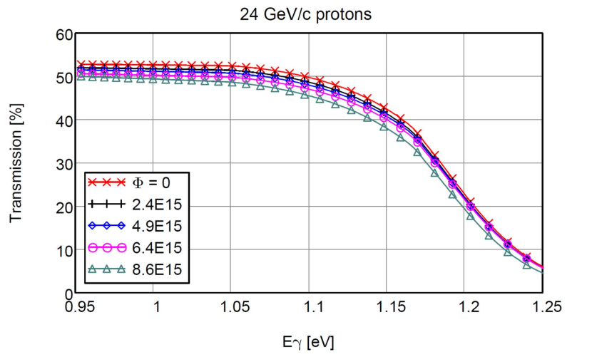
For the transmission measurements an Agilent CARY 5000 UV-VIS-NIR [8] was used. The wavelength range for the samples was 0.95 to , and for the 3 mm samples 0.95 to . Fig. 1 shows the transmission measured at a temperature of about 295 K as a function of the photon energy, [eV] = 1.24.
For the isochronal annealing the 3 mm samples were heated for 15 min to temperatures of (80, 100, 120, 150, 180, 210) ∘C.

From the measured transmission, , the absorption coefficient, , is obtained using the standard formulae [3]:
| (2) |
with and . The thickness of the sample is , is the reflection of a single air-silicon interface, the corresponding transmission, and the index of refraction of silicon taken from [4], which is assumed not depend on the irradiation fluence.
3 Analysis of the absorption data for non-irradiated silicon
In this section, it is investigated if Eq. 1 is able to describe the absorption data of non- irradiated silicon from the literature. It is found that this is not the case and a different method for extracting and is proposed.
Inspecting Eq. 1 reveals that as function of is expected to be zero for , a straight line for , where the second term is zero, followed by a second straight line for , where the second term dominates. For this reason it is customary to look at .

The data at 25 ∘C [4] are fitted by Eq. 1, with , , , and the normalisation as free parameters. For 15 meV [9, 10] is used. Table 1 and Fig. 2 present the results. Qualitatively, the data agree with the expectation of two straight lines, however the fit is not able to describe the data quantitatively. In addition, significant differences to the generally accepted values of eV [11, 12], and meV [13, 9] are observed. The value obtained from the fit of , which is constrained by the ratio of the two slopes of , is quite compatible with the temperature 296.15 K of the transmission data used in the analysis.
| [eV] | [meV] | [K] | |
|---|---|---|---|
| Literature | 296.15 | ||
| Fit to | 1.1105 | 49.3 | 275.8 |
| d | 1.1212 | 59.1 | – |
The poor description of the data can be ascribed to additional contributions to the absorption or to scattering. Already for below phonon absorption, the value of is finite. Under the assumption that these additional contributions have smooth derivatives at the onsets of phonon absorption and phonon emission, steps in the slope d should hardly be affected, and maxima in d should appear at and . Anticipating fluctuations for the measured values, the following procedure, called smoothed derivative method, is proposed:
-
1.
Convolve with a Gaussian with variance .
-
2.
Calculate numerically the second derivative of the convolved distribution.
-
3.
Associate of the lower, dominant peak with , and the upper one with .
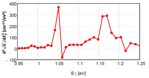
Fig. 3 shows the smoothed second derivative using meV. The results are not sensitive to the choice of . Narrow peaks are observed at eV and at 1.17 eV. Their precise values are obtained from the values of at which the derivatives of d cross zero. Table 1 presents the results. The value of agrees with the literature values, and the value of is 2.8 meV lower, which can be considered satisfactory. For the data discussed in the next section, the differences are 1 meV only, which is well within the uncertainties of the literature values of .
4 Analysis of the measured transmission data
In this section, the smoothed derivative method introduced in Sect. 3 is used to extract the values of and from the measured transmission data.
The data, for the different silicon thicknesses and values, are shown in Fig. 4. It is noted that for the mm samples shown in Fig. 4(b), the transmission for eV is below 0.01 % and the measurements are dominated by noise. It can also be seen that already for eV, which is the photon energy required for the excitation of an electron from the valence to the conduction band by the absorption of a transverse optical phonon, the value of is finite and increases with fluence. This increase is ascribed to the absorption by states in the band gap. As the and dependence of this contribution is not known, a fit using Eq. 1 is problematic.
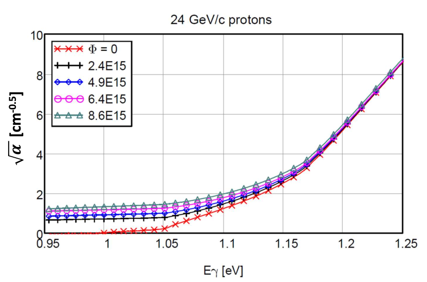
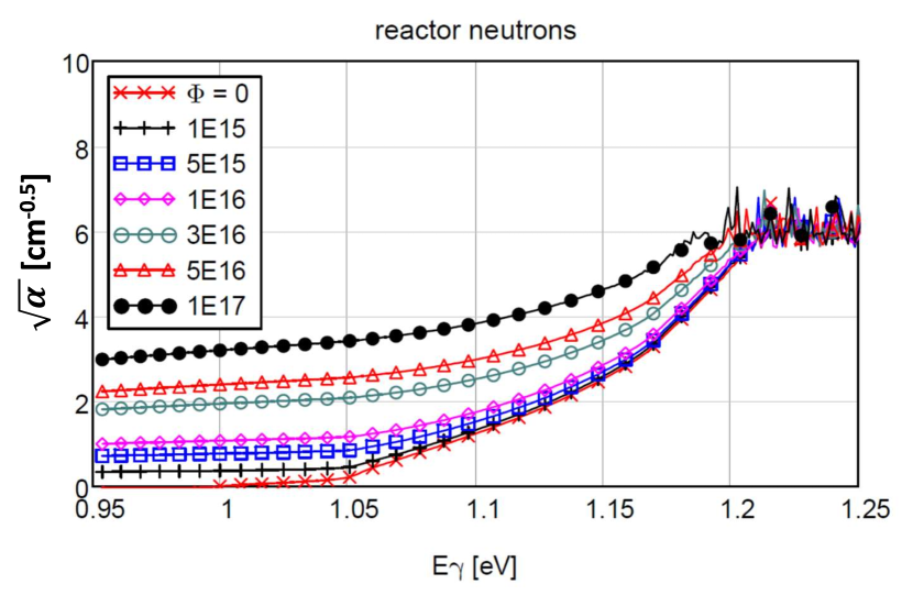
Fig. 5 shows the smoothed second derivative of the data of Fig. 4 using the value meV for the Gauss convolution. Like for the data of non-irradiated silicon, sharp peaks are observed at eV and 1.17 eV. The results are not sensitive to the choice of . For the data the noise in the transmission measurements for eV causes oscillations of the second derivative and the results for the 1.17 eV peak can not be trusted.

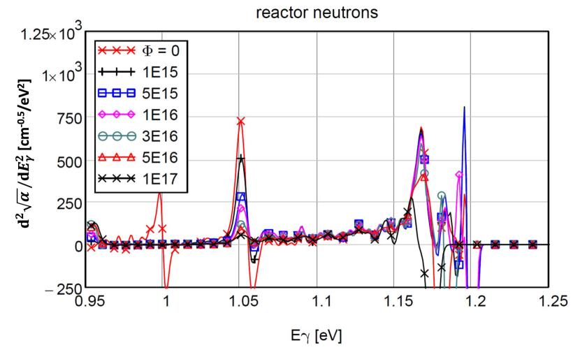
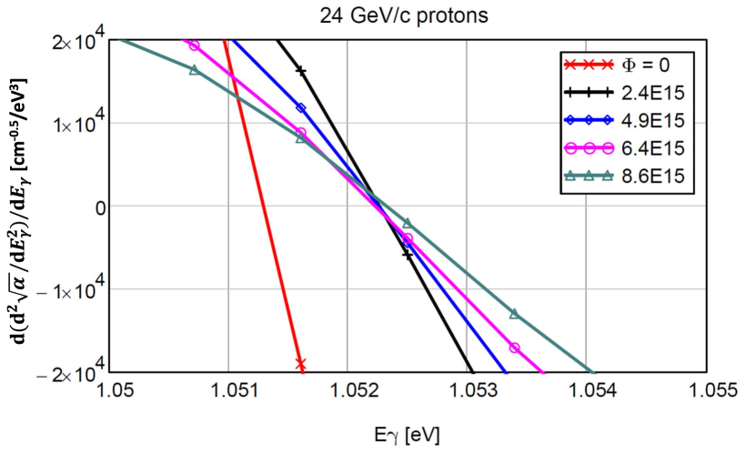
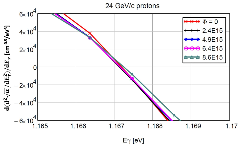
The precise peak positions are determined by the zero crossing of the first derivative of d. Examples in an expanded scale for the data with proton irradiation are shown in Fig. 6. For the phonon emission region, shown in Fig. 6(b), the zero crossings are within meV. For the phonon absorption region, shown in Fig. 6(a), with the exception of the data, the zero crossings are also within meV. The agreement of the peak positions of d within a fraction of 1 meV is remarkable. The results for the data with neutron irradiation are similar. From the values for phonon absorption and for phonon emission, and are determined:
| (3) |
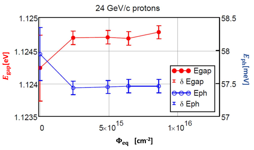
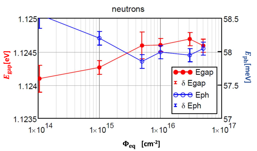
The results for the dependence of using meV, and of are shown in Fig. 7. It can be seen that within the fluctuations of the results, which are well below 1 meV, neither nor depend on . The systematic uncertainty due to the uncertainties of the transmission and wave-length scales of the spectral photometer is estimated to be 1 meV, and the statistical uncertainty of the peak determination using the smoothed derivative method 0.2 meV.
The values of eV and meV agree with the values from literature.
The values for the neutron irradiation with are not shown, because noise prevents the determination of . However, the value of eV agrees with the values at lower fluences. Finally, it is mentioned that the analysis of the 15 min-isochronal annealing data between 80 and 210 ∘C shows that and do not change with annealing.
To summarize this section:
The smoothed derivative method has been used to investigate if and of silicon change after irradiation with energetic protons and reactor neutrons. It is found that up to the investigated fluence of possible changes of and are less than meV. The values of and agree with the literature values at the 1 meV level.
5 Band-gap energy in clusters
Until now, the question, if the band-gap energy differs inside and outside of damage clusters, has not been answered. Problems are the large fluctuations of the cluster sizes and shapes, the poor knowledge of the cluster introduction rates and a probable dependence of on the position within a cluster. In the following this question is addressed in a highly simplified approach:
-
1.
The clusters are assumed to have an average volume ; it is estimated assuming that the cluster has the shape of a tube of length and radius : . Inside of this volume the constant value is assumed for the energy band-gap, and outside , the value measured for non-irradiated silicon; is the difference of the band-gap energy inside and outside of a cluster.
-
2.
The cluster density is assumed to be , with the cluster-introduction rate .
-
3.
The probability that the photon converts within a cluster is estimated using Poisson statistics: .
-
4.
From the values of determined in Sect. 4, is obtained.
Finally, the formula used for estimating the energy-gap difference inside and outside of clusters is:
| (4) |
As the density of cluster increases with , the sensitivity for increases with , and the data are used in the following. From the data an upper limit of 0.5 meV for the difference is obtained. For its determination, the energy threshold for phonon absorption, , had to be used as at this fluence noise does not allow to determine the threshold for phonon emission. It should be noted that, as also seen in Fig. 7, above the change of is 0.1 meV only, and the unexpected increase at lower values is probably an artifact of the analysis procedure.
A value for the cluster introduction rate by 1 MeV neutrons is extracted from Figs. 5 and 7 of [14]. For the cluster shapes, tubes of length and radius are assumed. From [14] the value nm is estimated. The value nm is obtained from , with the Bohr radius of the hydrogen atom, nm, the relative dielectric constant of silicon, , and the ratio of the effective to the free electron mass for silicon. The estimation of is the back-of-the-envelope estimation of the effective radius of the electron cloud of donor atoms in silicon, resulting in . This value has a large uncertainty, which is also reflected by the numbers found in the literature, e. g. 3 800 nm3 in [15], and 18 000 nm3 in [16].
Inserting these numbers into Eq. 4 results in values of meV for meV, and a probability that the photon interacts inside a cluster of 4.4 %.
These values can be compared to the results of [17], where the change of the excitation energy, , of damage states in clusters produced by 27 MeV electrons has been investigated using TSC measurements. For the double vacancy the value meV was determined. It could also be shown that by annealing, approaches zero, which was taken as evidence that the clusters anneal. The change of has contributions from the electrostatic repulsion of charged states in the cluster, but can also come from a possible change of the energy-band gap. The values of are similar to the upper limits on obtained in this study, and thus can not answer the question how much a possible change of the band-gap energy contributes to .
6 Conclusions
The main results of the paper are:
-
1.
A method has been developed which allows to precisely locate kinks, i. e. sudden changes of the derivative as produced by thresholds, in measured spectra.
-
2.
The method is used to extract the band-gap energy, , and the energy of transverse optical phonons, , from optical transmission measurements of crystalline silicon irradiated by energetic protons and reactor neutrons to fluences up to .
-
3.
Within the 0.5 meV accuracy, and do no change with irradiation fluence, and the values agree with results from literature.
To the authors’ knowledge, the method of determining the photon energies for phonon absorption, , and phonon emission, , from peaks in the second derivative of smoothed with a Gaussian kernel, has not been used so far. The accuracy achieved for and is well below 1 meV, and this method can be used to precisely determine the band-gap energy and the energy of the phonons required to excite an electron from the valence to the conduction band in indirect semi-conductors, like silicon. The results are hardly affected by the presence of light-absorption centers. For the measurements presented in this paper they are caused by the radiation damage of crystalline silicon by hadrons and dominate the absorption for the highest irradiation fluences investigated.
For determining , the difference of the band-gap energy inside and outside of clusters, the cluster introduction rate and the cluster shapes have to be known. Only crude estimates of these parameters are available, and the upper limit of meV determined for has large uncertainties.
Acknowledgements
We thank Lukas Terkowski from the group of Roman Schnabel of the Institute of Laser Physics of Hamburg University for his help with the photo-spectrometer measurements, and Vladimir Cindro and Gregor Kramberger for the neutron irradiations performed at the TRIGA reactor of the Jozef Stefan Institute, Ljubljana. The work was partially supported by the Deutsche Forschungsgemeinschaft (DFG, German Research Foundation) under Germany’s Excellence Strategy – EXC 2121 Quantum Universe – 390833306, and by the "Partnership for Innovation, Education and Research (PIER)" between DESY and the University of Hamburg."
References
References
- [1] P.Y. Yu and M. Cordona, Fundamentals of Semiconductors: Physics and Material Properties, Berlin Heidelberg, 2010, ISBN: 978-3-662-51736-9.
- [2] Chin-Yi Tsai, Absorption coefficients of silicon: A theoretical treatment, Journal of Applied Physics 123 (2018) 183103.
- [3] C. Scharf, F. Feindt, R. Klanner, Influence of radiation damage on the absorption of near-infrared light in silicon, Nuclear Instruments and Methods in Physics Research A 968 (2020) 163955.
- [4] M.A. Green, Improved silicon optical parameters at 25 ∘C, 295 K and 300 K including temperature coefficients, Pholtovolt. Res. Appl. 2021:1–16.
- [5] F. Ravotti, M. Glaser, M. Moll, Upgrade of the Proton Irradiation Facility in the CERN PS EAST AREA, https://cds.cern.ch/record/1951308.
- [6] M. Moll et al., Relation between microscopic effects and macroscopic changes in silicon detector properties after hadron irradiation, Nuclear Instruments and Methods in Physics Research B 186 (2002) 100–110.
- [7] K. Ambrozic, G. Zerovnik, L. Snoj, Computational analysis of the dose rates at JSI TRIGA reactor irradiation facilities, Applied Radiation and Isotopes 130 (2017) 140–152.
- [8] www.agilent.com.
- [9] K.L. Shaklee and R.E. Nahory, Valley-Orbit Splitting of Free Excitons? The Absorption Edge of Si, Phys. Rev. Letters 24 (17) (1970) 942–945.
- [10] M.A. Green, Improved value for the silicon free exciton binding energy, AIP Advances 3 (2013) 112104.
- [11] W. Bludau, A. Onton and W. Heinke, Temperature dependence of the band gap of silicon, Journal of Applied Physics 46 (1974) 1846–1848.
- [12] S. Bensalem, M. Chegaar, A. Herguth, Band gap dependence with temperature of semiconductors from solar cells electrical parameters, Current Applied Physics 17 (2017) 55–59.
- [13] A.G. Chynoweth, R.A. Logan, D.E. Thomas, Phonon-assisted tunneling in silicon and germanium Esaki junctions, Physical Review 125 (1962) 877–881.
- [14] M. Huhtinen, Simulation of non-ionising energy loss and defect formation in silicon, Nuclear Instruments and Methods in Physics Research A 491 (2002) 194–215.
- [15] V.A.J. van Lint, R.E. Leadon and J.F. Colwell, Energy dependence of displacement effects in semiconductors, IEEE Trans. Nucl. Science NS-19 (6) (1972) 181–185.
- [16] R.R. Holmes, Carrier removal in neutron irradiated silicon, IEEE Trans. Nucl. Science NS-17 (6) (1970) 137.
- [17] E.M. Donegani et al., Study of point and cluster defects in radiation-damaged silicon, Nuclear Instruments and Methods in Physics Research A 898 (2018) 15–23.