Berry curvature dipole senses topological transition in a moiré superlattice
Topological aspects of electron wavefunction play a crucial role in determining the physical properties of materials. Berry curvature and Chern number are used to define the topological structure of electronic bands. While Berry curvature and its effects in materials have been studied [1, 2], detecting changes in the topological invariant, Chern number, is challenging. In this regard, twisted double bilayer graphene (TDBG) [3, 4, 5, 6, 7] has emerged as a promising platform to gain electrical control over the Berry curvature hotspots [8] and the valley Chern numbers of its flat bands [9, 10]. In addition, strain induced breaking of the three-fold rotation () symmetry in TDBG, leads to a non-zero first moment of Berry curvature called the Berry curvature dipole (BCD), which can be sensed using nonlinear Hall (NLH) effect [11]. We reveal, using TDBG, that the BCD detects topological transitions in the bands and changes its sign. In TDBG, the perpendicular electric field tunes the valley Chern number and the BCD simultaneously allowing us a tunable system to probe the physics of topological transitions. Furthermore, we find hysteresis of longitudinal and NLH responses with electric field that can be attributed to switching of electric polarization in moiré systems. Such a hysteretic response holds promise for next-generation Berry curvature-based memory devices. Probing topological transitions, as we show, can be emulated in other 3D topological systems.
Exploring materials with new topological phases and probing their symmetries has been at the forefront of modern research. Topology is often characterized by Berry curvature that manifests as quantum Hall effect [1] or as anomalous Hall effect in magnetic materials [1, 2]. While these effects have led to many breakthroughs in physics, these linear responses vanish in systems that preserve time-reversal symmetry. However, even in time-reversal symmetry protected systems, broken inversion symmetry can lead to the first moment of Berry curvature, namely Berry curvature dipole (BCD), when further spatial symmetries are reduced [11]. In presence of an ac current (of frequency ) in such system, the BCD can drive a second-order electrical response, namely the nonlinear Hall (NLH) voltage with zero (DC) and second-harmonic () frequency. Aligned with the recent interest in various nonlinear phenomena such as nonlinear optics, there is a rapidly growing interest to look for quantum materials that host the NLH effect [12, 13].
The topological phase of quantum materials can be characterized by the band-specific topological invariant Chern number. Often systems undergo transition between topological phases and these transitions are hard to detect, unlike phase transitions of order parameter. Recent proposals suggest that topological transitions are accompanied by simultaneous changes in BCD [14, 15]. Moiré systems are known to be natural candidates to host topological bands [16]. While the NLH effect has been observed for transition metal dichalcogenides (TMDCs) [17, 18, 19, 20, 21] and corrugated bilayer graphene [22], the experimental study in two-dimensional moiré systems is limited [23]. Furthermore, topological transitions along with BCD have not been experimentally observed thus far.
Recently, the observation of several novel phenomena in moiré systems such as magic-angle twisted bilayer graphene has attracted attention [24, 25, 26, 27, 28, 29]. Flat bands in twistronic systems give rise to various electron correlation phenomena such as Mott insulators and superconductivity [24, 25, 26, 27]. In particular, the observation of anomalous Hall effect and orbital ferromagnetism point to the rich topology of these twisted systems [28, 29]. Flat bands of moiré systems are also susceptible to symmetry breaking by strain [30]. Together with the fact that spatial symmetry breaking can lead to nonzero BCD [30, 31, 32], bands in 2D moiré systems offer an interesting platform to electrically tune topology and detect it via the NLH effect.
In this work, we use twisted double bilayer graphene (TDBG), in which two copies of bilayer graphene are stacked together with a small twist angle 1.1∘, as a candidate system to study topological transitions using the NLH effect. While the flat bands in TDBG host correlation induced physics as in twisted bilayer graphene, TDBG is additionally equipped with electric field tunability [3, 4, 5, 6, 7, 33]. The perpendicular electric field, apart from modulating the band structure, can also change the valley Chern number of a flat band [10]. Additionally, almost touching flat bands with small tunable energy gaps of few meV in TDBG gives rise to large Berry curvature in this system [16, 34, 8]. We use electric field tunability to demonstrate that TDBG hosts substantially large BCD due to strain. The BCD changes sign abruptly and this can be attributed to a topological transition, a change in valley Chern number, with the electric field. Additionally, hysteresis in both longitudinal resistance and NLH signal as a function of the electric field suggests switching between metastable states.
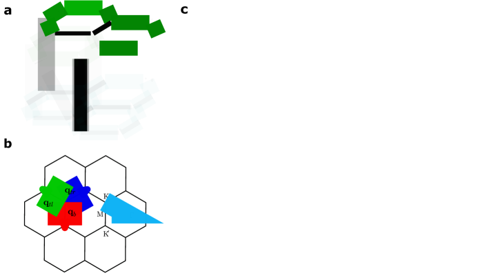
In TDBG, broken inversion symmetry allows nonzero Berry curvature (). Additionally, imaging of small-angle twisted moiré devices reveals strain that breaks three-fold rotational () symmetry [35, 23, 36]. Such reduced symmetry makes the Berry curvature distribution non-symmetric and anisotropic over the moiré Brillouin zone (mBZ), leading to nonzero BCD () given by,
| (1) |
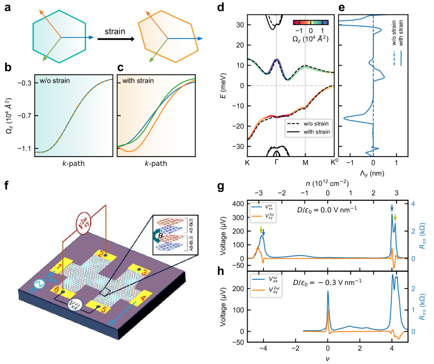
Here stands for the spatial index , is the energy of the band and is the Fermi-Dirac function. In Eq. (1), a sum over all the bands crossing the Fermi energy is implied. To calculate the BCD in TDBG, we consider distorted hexagonal moiré Brillouin zone with the symmetry broken by strain as shown in the schematic of Fig. 1a. The effect of symmetry breaking is reflected in the Berry curvature plots of Fig. 1b, c. Figure 1d shows the band structure for TDBG with a twist angle of 1.10∘ under 0.1% strain with of the flat bands indicated by the color. Together, nonzero Berry curvature and broken symmetry generate a nonzero BCD, as shown in Fig. 1e (see Methods and Supplementary Information section I-III for calculations).
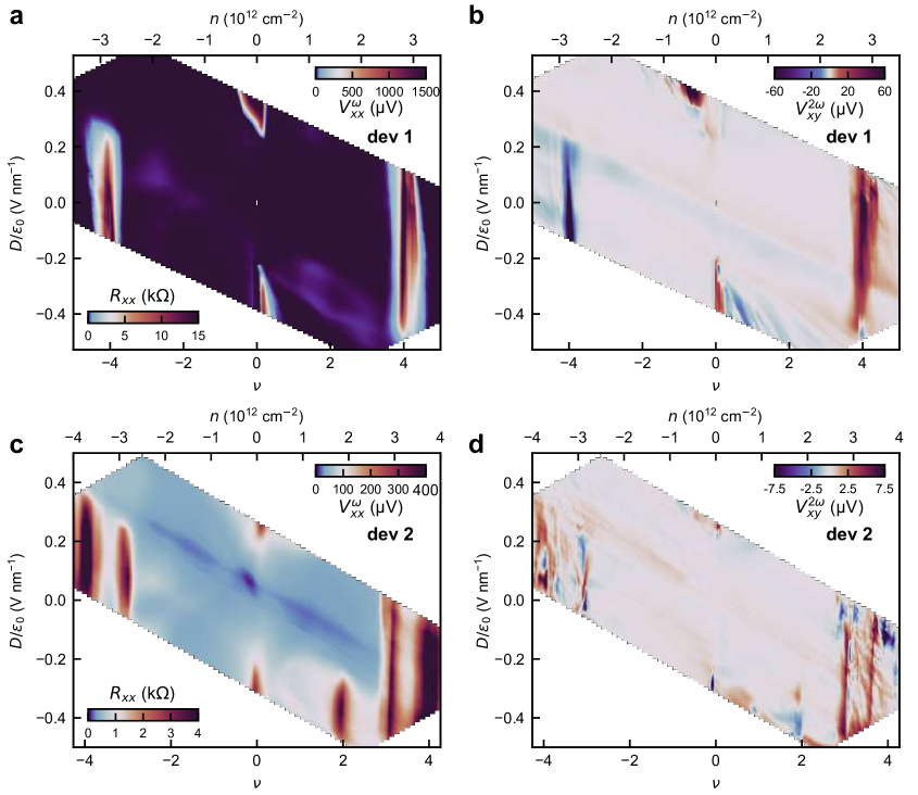
We fabricate multiple TDBG devices to measure NLH voltage, which probes the BCD [11, 18]. The dual-gate geometry allows independent control of the charge density and the perpendicular electric displacement field (see Methods). Figure 1f shows our measurement schematic to probe NLH effect. We send a current with low-frequency and measure the longitudinal voltage () and the second-harmonic NLH voltage () at frequencies and , respectively. In Fig. 1g, we show and as a function of moiré filling factor at zero displacement field for a TDBG device with twist angle 1.10∘. Here with representing the number of carriers to fill one moiré band and factor 4 due to four-fold degeneracy of spin and valley. Peaks in at correspond to the two moiré gaps. The substructures in the peaks of (indicated by arrows) result from slightly different twist angles, indicating an angle inhomogeneity of – a signature of strain [36] that causes BCD in our system. In Fig. 1h, we plot and for a non-zero perpendicular displacement field that creates a gap at (charge neutrality point, CNP). We find NLH voltage is high in the vicinity of band edge around the moiré gaps at and the CNP gap in our strained TDBG devices.
We now study the evolution of and the corresponding resistance () in the experimentally accessible parameter space of and in Fig. 2a. Schematics adjacent to Fig. 2a show change in the underlying band structure with (see Supplementary Information section III for calculated band structure). A finite displacement field opens up a gap at CNP between the conduction and the valence flat bands. These flat bands are separated from the remote moiré bands by two moiré gaps, which close at larger values of . Apart from the peaks in corresponding to the CNP gap at and the moiré gaps at , we observe other features like the cross towards the hole side () and the halo around V nm-1 towards the electron side (). These characteristic features of TDBG within partial fillings of the flat bands are likely to be connected to structures in the density of states [33].
Figure 2b shows the evolution of the NLH voltage in the same parameter space of and . In Fig. 2c, we have plotted few line slices of around for different . We find that peaks near the gaps at (CNP gap) and (moiré gaps). The coincidence of the NLH voltage with the TDBG bandgaps reveals that the Berry curvature hotspots, and hence the BCD, reside predominantly in the vicinity of the band edges. We explore this behavior further in Fig. 3.
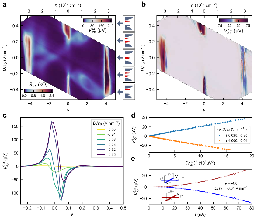
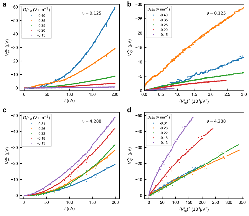
that we measure should scale quadratically with the in-plane ac electric field of frequency . To verify the quadratic scaling, we plot against the square of simultaneously measured for two different () biasing points in Fig. 2d. The linear behavior of with the square of confirms the quadratic scaling near both the CNP gap and the moiré gaps. Additionally, switches sign when we reverse the Hall voltage probes and the direction of current simultaneously as depicted in Fig. 2e. These observations clearly demonstrate the second-order nature of the measured NLH voltage, .
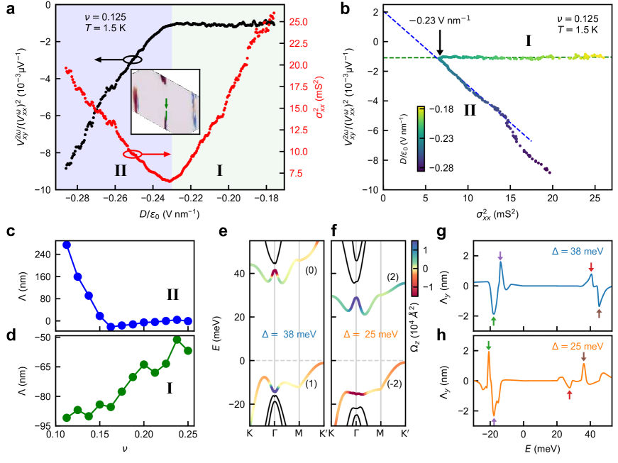
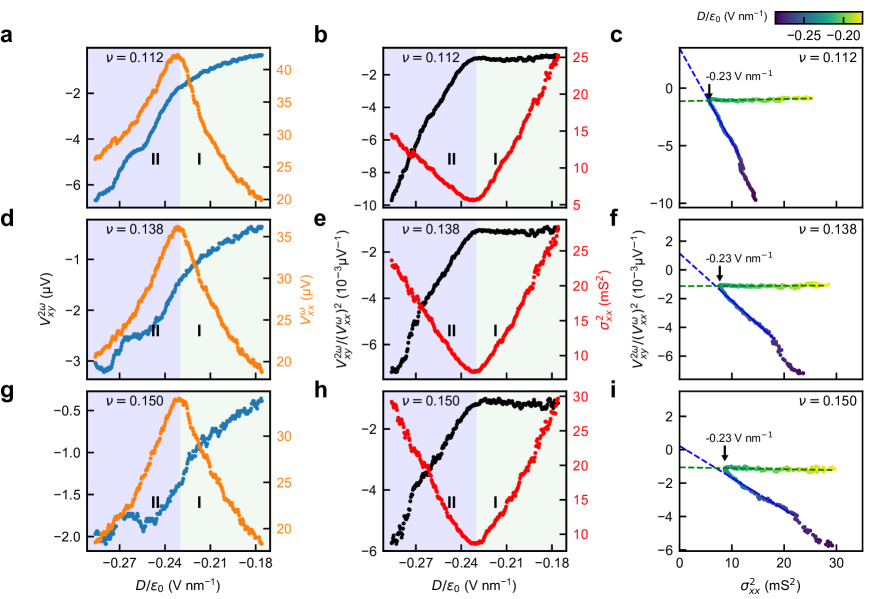
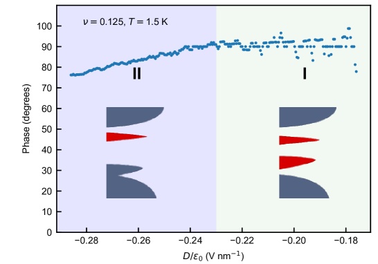
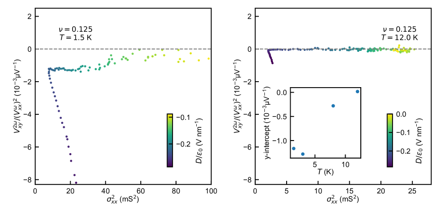
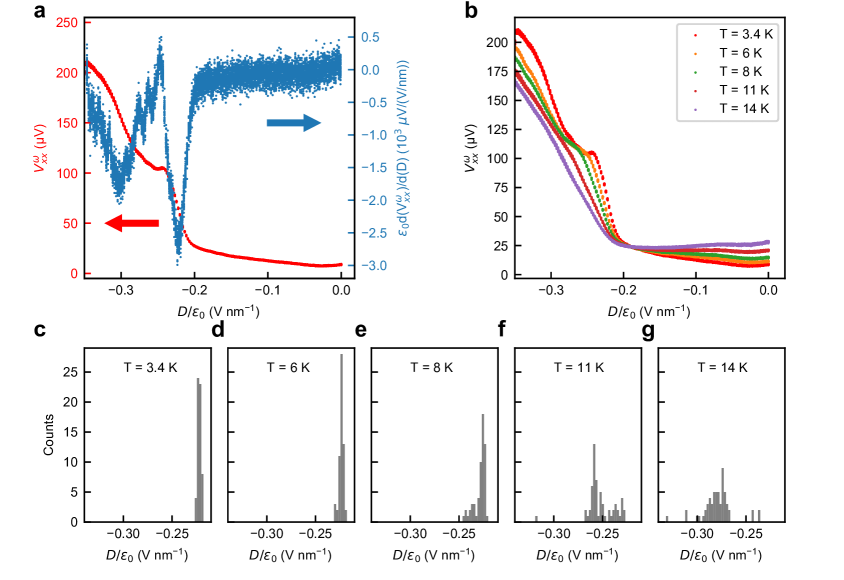
Having established as NLH voltage, we now use as a parameter to study scaling between normalized NLH voltage /()2 and square of longitudinal conductivity (). Such scaling can be used to quantify BCD, as discussed later. In Fig. 3a, we plot /()2 (left axis) and (right axis) as a function of for (indicated by the green vertical line in inset of Fig. 3a). The metallic behavior at ensures that the Fermi energy is near the band edge (see Extended Data Fig. 3a for the temperature () dependence of ). Both /()2 and show different trends in two different regimes of the displacement field separated at V nm-1. Interestingly, the two regimes are characterized by different band structures– in regime-I, the flat bands are gapped and are isolated from the remote moiré bands, while in regime-II the valence flat band merges with the remote moiré band (see Methods and Extended Data Fig. 3b, c). It is known that changes in band structure due to lead to change in the valley Chern numbers of the bands [9, 10] which in turn should be reflected in the change in sign of the BCD [15].
To investigate the close connection of such topological transition with BCD, we first experimentally analyze the scaling between /()2 and and later present a detailed calculation. In Fig. 3b, we find linear scaling between /()2 and in both regime-I and regime-II. The slope of a linear /()2 vs. dependence characterizes the contribution from skew-scattering () process [37], while the BCD can be extracted from the -intercept [17, 37] (see Supplementary Information section VI). A fixed temperature assures that the contributions from skew-scattering or side-jump in the NLH effect are not tuned within the linear fitted regimes [38, 39]. Interestingly, near-zero slope in regime-I suggests that the skew-scattering contribution is minimal when the flat bands are isolated from the remote moiré bands.
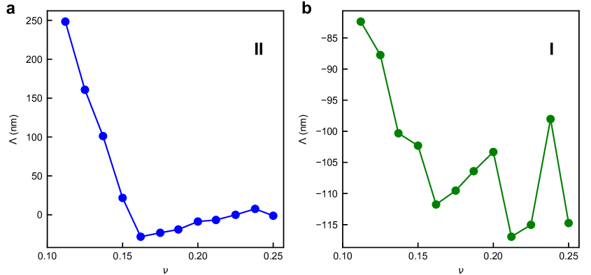
To distinguish the intrinsic BCD from other extrinsic contributions like side-jump, we repeat the scaling analysis for different fillings close to the band edge (see Extended Data Fig. 1). Figures 3c and 3d show the extracted BCD from regime-II and regime-I respectively. The drop in extracted BCD away from CNP (), consistent with Berry curvature hotspot peaking at the band edge, suggests that the NLH effect we observe is BCD dominated. The most striking observation, central to our study, is the sign change of BCD across the topological transition between regime-I and regime-II.
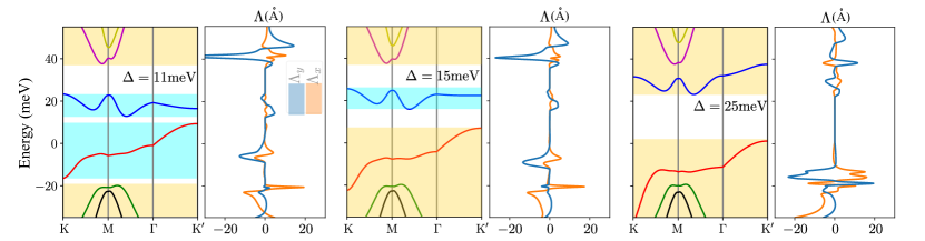
To theoretically verify the connection between BCD sign change and the topological transition, we calculate the band structure for two different values of inter-layer potential in Fig. 3e, f. A change in valley Chern number marks the topological transition. Consistently, the BCD changes sign as seen in Fig. 3h and 3g before and after the topological transition, respectively (also see Extended Data Fig. 4). We also note from Fig. 3e and 3f that the Berry curvature changes sign, around the -point, across the topological transition. Thus, the NLH effect acts as a good probe to detect topological transitions associated with the change in the valley Chern numbers [14].
We note that the BCD values in Fig. 3c, d are higher than the BCD observed in WTe2 [17, 18]. The scaling analysis using temperature as a parameter also gives a similar magnitude of BCD (see Extended Data Fig. 2). High BCD magnitude has been theoretically predicted in strained twisted systems [15, 23, 31, 30, 32]. The origin of high BCD in graphene-based moiré systems, in the vicinity of the charge neutrality point, can be understood using the model of strained twisted bilayer graphene as a tilted Dirac system [40]. In this model, BCD , where is the tilt parameter and is the moiré wavelength. So, the BCD is expected to be higher in moiré materials as compared to non-moiré materials like bilayer graphene, etc. (see Supplementary Information section V for details).
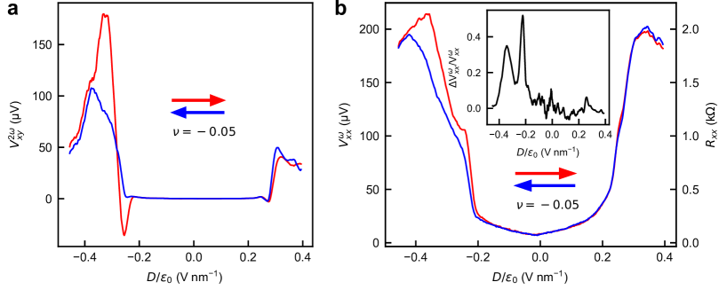
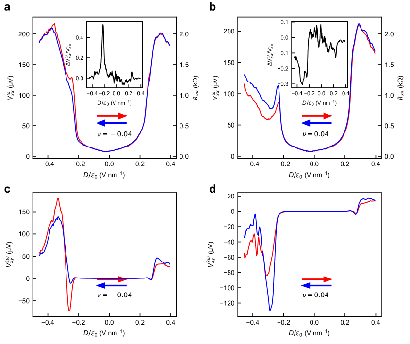
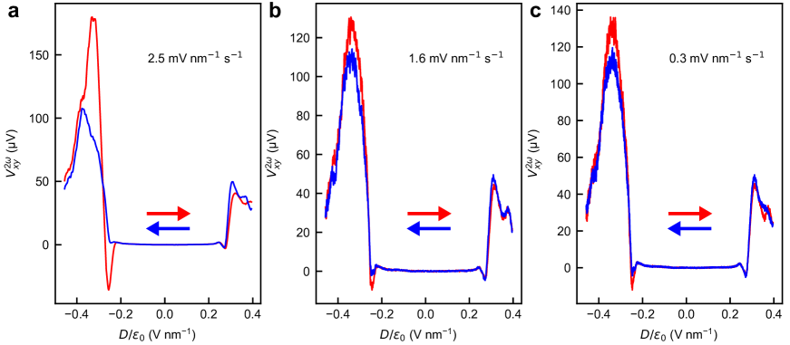
Finally, we examine the variation of NLH voltage at large displacement fields and, interestingly, observe a hysteretic response as shown in Fig. 4a. Fig. 4b shows the simultaneously measured , which also reveals hysteresis with . The sense of hysteresis is doping dependent (see Supplementary Information section X.4) and cannot be explained by charge traps in dielectric. See Supplementary Information section X for temperature effects, rate dependence, and switching statistics of the hysteresis. The inset of Fig. 4b shows the difference in for up and down sweeps. Intriguingly, the hysteresis is maximal around V nm-1 where a topological transition takes place as shown in Fig. 3b. However, more studies are required for a full microscopic understanding.
Our experimental data suggest the existence of metastable states; the origin of these states can be due to two possible mechanisms. Firstly, metastable polarization states in the system can arise from a difference in charge density across layers due to symmetry breaking in the device geometry (see Methods for further discussion). Secondly, flexoelectric coupling between perpendicular electric field and the strain gradient across the domain interfaces can lead to electric polarization in moiré systems [41]. Polarization from both possible mechanisms can lead to change in strain profile that can be further pinned by defects; this can account for the hysteresis we observe. Strain and polarization, through the effective electric field, modify the band structure and hence the value of and .
Tunable BCD values, together with the coupling of BCD to hysteresis in the same platform, as we demonstrate using TDBG, may open new frontiers for next-generation memory devices. In general, probing topological transitions using electrical transport is challenging. Our experiment demonstrates that the NLH effect can probe topological transitions. Electric field tunable band structure of few-layer heterostructures provides a useful way for probing topological transitions, as we show using TDBG. Our approach to detect topological transitions using NLH effect is applicable for 3D systems as well.
Acknowledgements:
We thank Justin Song, Abhay Pasupathy, Senthil Todadri, Biswajit Datta, Sanat Ghosh, and Supriya Mandal for helpful discussions and comments. We thank Surya Kanthi R. S., Joydip Sarkar, Krishnendu Maji, and Raghav Dhingra for experimental assistance. M.M.D. acknowledges Nanomission grant SR/NM/NS-45/2016 and DST SUPRA SPR/2019/001247 grant along with Department of Atomic Energy of Government of India 12-R&D-TFR-5.10-0100 for support. K.W. and T.T. acknowledge support from the Elemental Strategy Initiative conducted by the MEXT, Japan (Grant Number JPMXP0112101001) and JSPS KAKENHI (Grant Numbers 19H05790 and JP20H00354). A.A. acknowledges IIT Kanpur - India, Science Engineering and Research Board (SERB)- India, and the Department of Science and Technology (DST) - India, for financial support. A.C. acknowledges the Institute Post-Doctoral fellowship of IIT Kanpur. K. Das acknowledges IIT Kanpur for Senior Research Fellowship. A.A., A.C., and K. Das also thank CC-IIT Kanpur, for the high-performance computing facility. K. Debnath is grateful to the Jawaharlal Nehru Centre for Advanced Scientific Research, India, for a research fellowship. U.V.W. acknowledges support from a JC Bose National Fellowship of SERB-DST.
Data Availability:
The experimental data used in the figures of the main text are available in Zenodo with the identifier doi:10.5281/zenodo.5211285 [42]. Additional data related to this study are available from the corresponding authors upon reasonable request.
Author Contributions:
S.S., P.C.A., and L.D.V.S. fabricated the devices. S.S. and P.C.A. did the measurements and analyzed the data. A.C., K. Das, and A.A. did the band structure, BCD and Chern number calculations. K. Debnath and U.V.W. did the polarization calculations. K.W. and T.T. grew the hBN crystals. S.S., P.C.A., A.A., and M.M.D. wrote the manuscript with inputs from everyone. M.M.D. supervised the project.
Competing Interests:
The authors declare no competing interests.
References
- [1] Xiao, D., Chang, M.-C. & Niu, Q. Berry phase effects on electronic properties. Reviews of Modern Physics 82, 1959–2007 (2010).
- [2] Nagaosa, N., Sinova, J., Onoda, S., MacDonald, A. H. & Ong, N. P. Anomalous Hall effect. Reviews of Modern Physics 82, 1539–1592 (2010).
- [3] Burg, G. W. et al. Correlated insulating states in twisted double bilayer graphene. Physical Review Letters 123, 197702 (2019).
- [4] Shen, C. et al. Correlated states in twisted double bilayer graphene. Nature Physics 16, 520–525 (2020).
- [5] Adak, P. C. et al. Tunable bandwidths and gaps in twisted double bilayer graphene on the verge of correlations. Physical Review B 101, 125428 (2020).
- [6] Cao, Y. et al. Tunable correlated states and spin-polarized phases in twisted bilayer–bilayer graphene. Nature 583, 215–220 (2020).
- [7] Liu, X. et al. Tunable spin-polarized correlated states in twisted double bilayer graphene. Nature 583, 221–225 (2020).
- [8] Sinha, S. et al. Bulk valley transport and Berry curvature spreading at the edge of flat bands. Nature Communications 11, 5548 (2020).
- [9] Koshino, M. Band structure and topological properties of twisted double bilayer graphene. Physical Review B 99, 235406 (2019).
- [10] Zhang, Y.-H., Mao, D., Cao, Y., Jarillo-Herrero, P. & Senthil, T. Nearly flat Chern bands in moiré superlattices. Physical Review B 99, 075127 (2019).
- [11] Fu, L. & Sodemann, I. Quantum nonlinear Hall effect induced by Berry curvature dipole in time-reversal invariant materials. Physical Review Letters 115, 216806 (2015).
- [12] Ma, Q., Grushin, A. G. & Burch, K. S. Topology and geometry under the nonlinear electromagnetic spotlight. Nature Materials 20, 1601–1614 (2021).
- [13] Du, Z. Z., Lu, H.-Z. & Xie, X. C. Nonlinear Hall effects. Nature Reviews Physics 3, 744–752 (2021).
- [14] Facio, J. I. et al. Strongly enhanced Berry dipole at topological phase transitions in BiTeI. Physical Review Letters 121, 246403 (2018).
- [15] Hu, J.-X., Zhang, C.-P., Xie, Y.-M. & Law, K. T. Nonlinear Hall effects in strained twisted bilayer WSe2. arXiv:2004.14140 [cond-mat] (2020).
- [16] Song, J. C. W., Samutpraphoot, P. & Levitov, L. S. Topological Bloch bands in graphene superlattices. Proceedings of the National Academy of Sciences 112, 10879–10883 (2015).
- [17] Kang, K., Li, T., Sohn, E., Shan, J. & Mak, K. F. Nonlinear anomalous Hall effect in few-layer WTe2. Nature Materials 18, 324–328 (2019).
- [18] Ma, Q. et al. Observation of the nonlinear Hall effect under time-reversal-symmetric conditions. Nature 565, 337–342 (2019).
- [19] Shvetsov, O. O., Esin, V. D., Timonina, A. V., Kolesnikov, N. N. & Deviatov, E. V. Nonlinear Hall effect in three-dimensional Weyl and Dirac semimetals. JETP Letters 109, 715–721 (2019).
- [20] Xiao, J. et al. Berry curvature memory through electrically driven stacking transitions. Nature Physics 16, 1028–1034 (2020).
- [21] Tiwari, A. et al. Giant c-axis nonlinear anomalous Hall effect in T-MoTe2 and WTe2. Nature Communications 12, 2049 (2021).
- [22] Ho, S.-C. et al. Hall effects in artificially corrugated bilayer graphene without breaking time-reversal symmetry. Nature Electronics 4, 116–125 (2021).
- [23] Huang, M. et al. Giant nonlinear Hall effect in twisted WSe2. arXiv:2006.05615 [cond-mat] (2021).
- [24] Kim, K. et al. Tunable moiré bands and strong correlations in small-twist-angle bilayer graphene. Proceedings of the National Academy of Sciences 114, 3364–3369 (2017).
- [25] Cao, Y. et al. Correlated insulator behaviour at half-filling in magic-angle graphene superlattices. Nature 556, 80–84 (2018).
- [26] Cao, Y. et al. Unconventional superconductivity in magic-angle graphene superlattices. Nature 556, 43–50 (2018).
- [27] Lu, X. et al. Superconductors, orbital magnets and correlated states in magic-angle bilayer graphene. Nature 574, 653–657 (2019).
- [28] Sharpe, A. L. et al. Emergent ferromagnetism near three-quarters filling in twisted bilayer graphene. Science 365, 605–608 (2019).
- [29] Serlin, M. et al. Intrinsic quantized anomalous Hall effect in a moiré heterostructure. Science 367, 900–903 (2020).
- [30] Zhang, C.-P. et al. Giant nonlinear Hall effect in strained twisted bilayer graphene. arXiv:2010.08333 [cond-mat] (2020).
- [31] Pantaleón, P. A., Low, T. & Guinea, F. Tunable large Berry dipole in strained twisted bilayer graphene. Physical Review B 103, 205403 (2021).
- [32] He, Z. & Weng, H. Giant nonlinear Hall effect in twisted bilayer WTe2. npj Quantum Materials 6, 101 (2021).
- [33] He, M. et al. Symmetry breaking in twisted double bilayer graphene. Nature Physics 17, 26–30 (2021).
- [34] Chebrolu, N. R., Chittari, B. L. & Jung, J. Flat bands in twisted double bilayer graphene. Physical Review B 99, 235417 (2019).
- [35] McGilly, L. J. et al. Visualization of moiré superlattices. Nature Nanotechnology 15, 580–584 (2020).
- [36] Kazmierczak, N. P. et al. Strain fields in twisted bilayer graphene. Nature Materials 20, 956–963 (2021).
- [37] He, P. et al. Quantum frequency doubling in the topological insulator Bi2Se3. Nature Communications 12, 698 (2021).
- [38] Xiao, C., Zhou, H. & Niu, Q. Scaling parameters in anomalous and nonlinear Hall effects depend on temperature. Physical Review B 100, 161403 (2019).
- [39] Du, Z. Z., Wang, C. M., Li, S., Lu, H.-Z. & Xie, X. C. Disorder-induced nonlinear Hall effect with time-reversal symmetry. Nature Communications 10, 3047 (2019).
- [40] Mannaï, M. & Haddad, S. Twistronics versus straintronics in twisted bilayers of graphene and transition metal dichalcogenides. Physical Review B 103, L201112 (2021).
- [41] Li, Y. et al. Unraveling strain gradient induced electromechanical coupling in twisted double bilayer graphene moiré superlattices. Advanced Materials 33, 2105879 (2021).
- [42] Sinha, S. et al. Experimental data for Berry curvature dipole senses topological transition in a moiré superlattice. Zenodo (2021).
METHODS
1 Device fabrication
We fabricate multiple dual gated TDBG devices. We have a metal top gate and SiO2(280 nm)/Si++ back gate. Dual gates allow us to independently control the charge density () and the perpendicular displacement field (), where and . Here, is the back (top) gate capacitance and is the voltage applied to the back (top) gate, respectively. is the electronic charge. To prepare the hBN/TDBG/hBN graphene stacks, we pre-cut bilayer graphene using a tapered optical fiber scalpel [1]. The detail fabrication and twist angle determination procedure is discussed in the methods of Ref. [8]. The twist angle is additionally confirmed via magneto-transport measurements.
2 Measurement technique
We send current using DS360 ultra-low distortion function generator. The chosen frequency for all the data is 177 Hz, except for Supplementary Fig. 8 where we vary the frequency. The voltages, and , are measured using SR830 lock-in amplifier in the first harmonic and second harmonic mode, respectively. In addition, to measure the DC voltage (Supplementary Fig. 20) generated due to the NLH effect, we use Keithley 2182 nanovoltmeter. For applying DC voltages to the top and back gate, we use NI DAQ. The temperature is measured using a sensor placed close to the device. The findings reported in the main manuscript are from a TDBG device with twist angle 1.10∘; other devices are shown in Supplementary Fig. 5 and 16.
3 BCD estimation
3.1 Using electric field as parameter
To extract out the BCD (), we use the formula , where is the second-order nonlinear electric field, is the in-plane longitudinal electric field, parallel to the direction of current, is the slope and is the intercept. Using the fact that the length and width of our device are 2 µm each, -intercept of vs. dependence. We fit the -parametric plot of vs. with a linear dependence (see Supplementary Information section VI for details) to extract and use the relation to estimate the BCD [17]. We assume that is 1% (limited by the energy scale set by the temperature 1.5 K) of the bandwidth (10 meV) of the flat band. To ensure that we place the Fermi energy within the flat band and not at the gap, we measure the temperature dependence of and find a metallic behavior irrespective of the chosen value of (see Extended Data Fig. 3a).
To verify the robustness of our observation of BCD sign change, we systematically show the scaling of normalized nonlinear Hall voltage (/()2) with square of longitudinal conductivity () for three different fillings () in Extended Data Fig. 1. Extended Data Fig. 1a, d, and g shows the measured nonlinear Hall voltage and longitudinal voltage as a function of the displacement field for three different . The background color denotes the two regimes– regime-I and regime-II, across which a topological transition occurs. We see broad peaks in across the critical electric field of V nm-1 in all three cases. Using the measured and as in Extended Data Fig. 1a, d, and g, we plot the corresponding normalized NLH voltage /()2 and (I/)2 as a function of displacement field for the three fillings in Extended Data Fig. 1b, e, and h. In Extended Data Fig. 1c, f, and i, we plot /()2 vs. , using displacement field as a parameter. The displacement field ( V nm-1), at which the change in sign of intercept occurs, remains invariant for different fillings. We extract the intercept and use it to estimate BCD as described above, and plot in Fig. 3c and 3d of the main manuscript.
The extracted BCD values from the two regimes are opposite in sign. A characteristic signature of a topological transition is a change in sign of BCD, as discussed in the main manuscript and also in Ref. [15] and Ref. [14]. As we show via resistance vs. temperature measurements in Extended Data Fig. 3c, displacement field closes the hole-side moiré gap around the same V nm-1. Displacement field, that causes the flat bands to touch the remote moiré valence bands, changes the valley Chern number of the bands in TDBG [9, 10], as we independently show in our calculations (Fig. 3e,f of the main manuscript) for the twist angle of 1.1∘. Such a change in sign of valley Chern number accounts for the two linear regimes with different signs of intercepts.
3.2 Using temperature as parameter
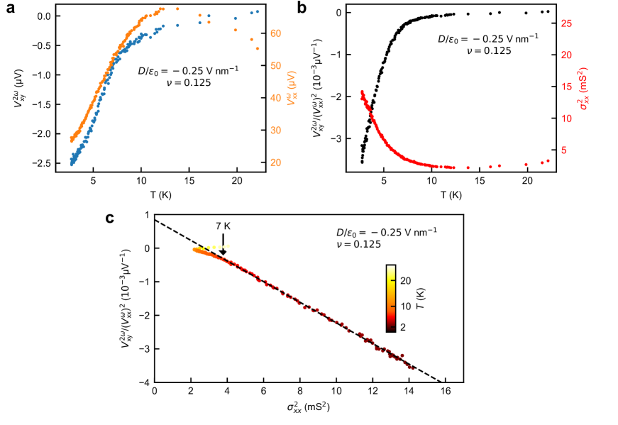
To independently confirm the order of magnitude of the estimated BCD, we also study the temperature dependence of the NLH voltage. In Extended Data Fig. 2, we show the scaling of normalized nonlinear Hall voltage (/()2) with the square of longitudinal conductivity () for the filling (the same for which we show a linear scaling, using displacement field as a parameter, in Fig. 3b of the main manuscript) and displacement field V nm-1. In Extended Data Fig. 2a, we show the temperature dependence of the NLH voltage (blue-colored data points) and longitudinal voltage (orange-colored data points). We see that goes close to zero at 20 K. In Extended Data Fig. 2b, we plot the temperature dependence of /()2 (black data points) and (red data points), using the data in Extended Data Fig. 2a. A decreasing with increasing temperature suggests that the filling corresponds to placing the Fermi level in the conduction flat band. In Extended Data Fig. 2c, we plot /()2 vs. , using temperature as a parameter and find similar linear dependence, as reported earlier [17], till K. The temperature regime is less than the Bloch-Grneisen temperature, ensuring that the other extrinsic contributions are not tuned in this temperature regime. A similar magnitude of -intercept in /()2 as in Fig. 3b of the main manuscript, suggests that BCD using temperature as a parameter is of similar magnitude that we get from parametric scaling of .
4 Inferring band structure using R vs. T dependence
In Extended Data Fig. 3, we show the temperature () variation of longitudinal resistance () for fillings at (corresponding to CNP in Extended Data Fig. 3b), (corresponding to conduction flat band edge in Extended Data Fig. 3a) and (corresponding to hole-side moiré gap in Extended Data Fig. 3c) at different displacement fields (). In Extended Data Fig. 3b, we see that as the magnitude of displacement field is increased, the slope of vs. changes from positive to negative, indicating a gap opening at CNP at a displacement field around of 0.2 V nm-1. This establishes that in regime-I, a gap at CNP persists between the red colored flat bands.
In Extended Data Fig. 3c, we see that as the magnitude of displacement field is increased, the slope of vs. changes from negative to positive, indicating a gap closing at the hole-side moiré gap at at a displacement field around of 0.23 V nm-1. This establishes that in regime-II, the hole-side moiré gap is closed and the flat band has merged with the hole-side remote moiré band.
5 Berry curvature dipole and topological transition
To investigate the topological phase-transition and associated sign reversal of Berry curvature dipole we have followed the low-energy continuum model approach of Bistritzer and MacDonald [2] for twisted bilayer graphene and extended it to TDBG (see Supplementary Information section I for details). The perpendicular electric field tunability of electronic band structure has been included in the Hamiltonian by a parameter , which represents constant potential gradient across the layers. The presence of finite strain in the fabricated TDBG sample breaks the symmetry (see Fig. 1a) which causes non-zero BCD. The uniaxial strain has been introduced into our model Hamiltonian as [3]
| (2) |
where a strain of magnitude is applied along a direction making angle with the zigzag direction of graphene. , the Poisson’s ratio is equal to for graphene. For our calculations, we have considered strain along the zigzag direction ().
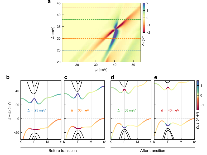
In Extended Data Fig. 4, we have plotted BCD as a function of inter-layer potential () and chemical potential () at a fixed strain value of . The butterfly structure signifies the evolution of BCD with the perpendicular electric field. The sign reversal of BCD near critical inter-layer potential meV indicates a topological transition. The upper panel of Extended Data Fig. 4 shows the -component of BCD in the conduction band side (). Before phase-transition, at 25 meV and 30 meV, the red lobe signifies the negative BCD for the first conduction band while the blue lobe represents positive BCD for moiré conduction bands. The corresponding band dispersions are shown in Extended Data Fig. 4b, c. The overlayed color indicates the Berry curvature hot spots within the band. After the phase-transition, at 38 and 43 meV, we observe positive lobe of BCD for the first conduction band while negative lobe for the higher conduction band. The corresponding dispersions are shown in Extended Data Fig. 4d, e. From the color map of Berry curvature, it is evident that in regime-I (before transition), the valence (conduction) band has a negative (positive) Berry curvature hotspot while it gets reversed in regime-II (after transition).
6 Metastable states in h-BN encapsulated twisted double bilayer graphene
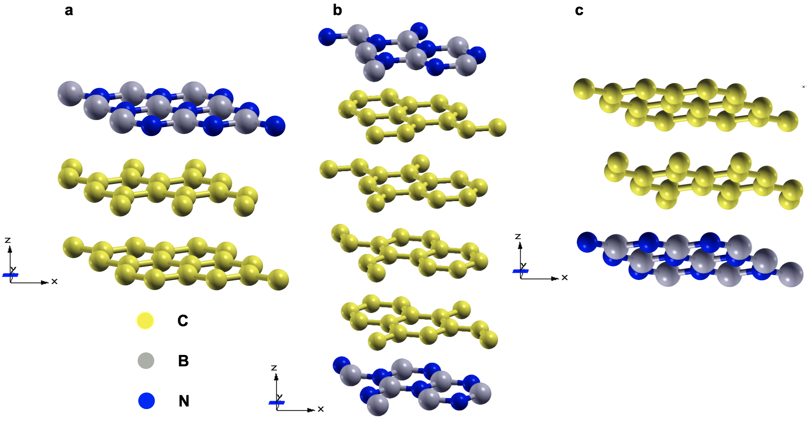
To identify the metastable states that possibly cause the observed hysteresis, we first present first-principles density functional theory analysis of a Gr-Gr-h-BN trilayer, which constitutes one of the halves which are twisted by a small angle in the TDBG. Interestingly, the outer h-BN monolayer breaks the sublattice-symmetry opening up a small gap at the Fermi level (see Extended Data Fig. 5a), accompanied by a weak layer asymmetry in the constitution of frontier electronic states (bands of pz orbitals) reflecting on an accumulation of a small electronic charge on one of the two graphene monolayers. This is expected from the lack of inversion or horizontal reflection symmetries in the trilayer, and our estimate of its polarization (along the -axis) is -0.34 C/cm2. We analyze effects of perpendicular electric field on the TDBG in two steps, focusing first on the coupling of field with the DBG (twist angle = 0) and then discuss the effect of twist in terms of variation in stacking between the DBGs. Using a rigid band model of frontier electronic states of DBG (for details of rigid band model refer to Supplementary Information section XI), we demonstrate that electric field permits switching to two metastable states with opposite polarization (Extended Data Fig. 5d) arising from the inversion of frontier electronic states in one of the DBGs (see Extended Data Fig. 5c). However, these states are symmetry equivalent and would not explain the hysteresis observed in resistances of TDBG, which we argue to arise from two mechanisms: (a) the inhomogeneous doping across the layers in the TDBG due to differences in the top and bottom doping as evident in our calculations of gated TDBG with a twist angle of 21.78o, and (b) switchable ferroelectric polarization associated with redistribution of regions with different stacking sequences (AA versus AB) across the twisted layers as shown in [4].
Our calculations of the TDBG (with 21.78o) with a bottom gate reveals the development of polarization upon doping with an estimate of 0.6 µC/cm2 (refer to Supplementary Fig. 19a). This is comparable to P 0.68 µC/cm2 of bilayered h-BN [4] and larger than that (P -0.18 µC/cm2) arising from the restructuring in terms of stacking sequence [5] in heterostructures. Thus, the observed hysteresis has possible contributions from inhomogeneous stacking as well as inhomogeneous, layer-dependent carrier concentration.
References
- [1] Varma Sangani, L. D. et al. Facile deterministic cutting of 2D materials for twistronics using a tapered fibre scalpel. Nanotechnology 31, 32LT02 (2020).
- [2] Bistritzer, R. & MacDonald, A. H. Moiré bands in twisted double-layer graphene. Proceedings of the National Academy of Sciences 108, 12233–12237 (2011).
- [3] He, W.-Y., Goldhaber-Gordon, D. & Law, K. T. Giant orbital magnetoelectric effect and current-induced magnetization switching in twisted bilayer graphene. Nature Communications 11, 1650 (2020).
- [4] Yasuda, K., Wang, X., Watanabe, K., Taniguchi, T. & Jarillo-Herrero, P. Stacking-engineered ferroelectricity in bilayer boron nitride. Science 372, 1458–1462 (2021).
- [5] Zheng, Z. et al. Unconventional ferroelectricity in moiré heterostructures. Nature 588, 71–76 (2020).

Supplementary Information
I Moiré flat bands in TDBG
To obtain the electronic band structure and related topological properties of the AB-AB twisted double bilayer graphene (TDBG) with twist angle we follow the continuum model approach of Bistritzer and MacDonald [1]. The AB-AB TDBG can be fabricated by placing two AB-stacked bilayer graphene (see the side view in Supplementary Fig. S1a) on top of each other and rotate the bilayers with respect to each other. For the band structure calculation, we assume that the upper bilayer () is rotated by an angle and the lower bilayer () is rotated by an angle adding to total twist angle . The smallest continuum Hamiltonian near the valley can be written as [34]
| (S1) |
Here, sign stands for the bilayer and represents the top (bottom) layer of each bilayer. Due to rotation, the Dirac Hamiltonian modifies as , where is the crystal momentum near the valley and are the Pauli matrices representing the sub-lattice degree of freedom of single-layer graphene. The effect of dimer site potential on each layer of a bilayer has been captured in the Hamiltonian by a parameter as . The inter-layer coupling matrix within each bilayer is represented as
where . The strong inter-layer coupling between the two dimer sites is denoted by (shown by solid line in Supplementary Fig. S1a), the inter-layer hopping between two non-dimer sites is denoted by (shown by dashed line in Supplementary Fig. S1a) and the inter-layer hopping between dimer and non-dimer sites is denoted by (shown by dotted line in Supplementary Fig. S1a). The various velocities can be calculated from the corresponding hopping amplitudes () using the conversion rule with Å. For our calculations, we consider the following parameters: the dimer site potential meV, the intra-layer hopping eV, which gives the Fermi velocity, m/s and meV. The remote hopping amplitudes and are considered to be meV and meV, respectively.
The moiré coupling between the twisted bilayers (coupling between the two adjacent rotated layers) in Eq. (S1) can be expressed as, . The hopping paths are given by the three vectors , ) and and the hopping matrices are given by,
| (S2) |
The diagonal () and off-diagonal () hopping strengths have been considered to be unequal due to the out-of-plane corrugation effect and chosen in the scale meV and meV, respectively. The tunability of the electronic band structure of the TDBG due to perpendicular electric field is included in the model Hamiltonian by means of inter-layer potential difference parameter . To model the effective electric field as a constant gradient in potential, we use == and ==.
II Impact of strain on electronic structure of TDBG
Equation (S1) and the corresponding band structure explain the measured resistance as a function of charge density and displacement field reasonably well. However, it can not account for the measured nonlinear Hall voltage due to the presence of symmetry in the continuum model. So to break the symmetry we include the effect of uniaxial strain quantified as [3]
| (S3) |
which breaks the symmetry [2, 3, 30, 15]. In Eq. (S3) is the strength of strain, is the Poisson ratio ( for graphene) and is the strain angle with respect to zigzag direction of graphene. The strain matrix has two fold impact on the model Hamiltonian—i) The Dirac points of bilayer gets shifted to DKA from with Å ) being the strain induced effective gauge field. As a result the moiré coupling vectors and the hopping matrices get modified. ii) The Dirac Hamiltonian itself modifies to . In our calculation we extend the strain implementation of Ref. [3] for twisted bilayer graphene to the TDBG where the hetero strain is applied solely on the lower bilayer.

The breaking of symmetry after strain implementation in the Hamiltonian is highlighted in Fig. 1b, c of the main manuscript where the Berry curvature () of the valence band is plotted along three paths arranged in 120∘ angle as shown by the blue, orange and green arrows in Fig. 1a of the main manuscript. The Berry curvature is calculated using the periodic part of the Bloch wave-function, , as
| (S4) |
In Supplementary Fig. S1c we have shown the Berry curvature distribution for the conduction (left column) and valence (right column) bands over the moiré BZ. Due to the broken symmetry, the distribution of Berry curvature in the -space becomes non-symmetric. Such non-symmetric Berry curvature in the moiré Brillouin zone (mBZ) recently has been shown to cause nonlinear Hall effect which is quantified by Berry curvature dipole (BCD) defined as
| (S5) |
Here, is the band index, is the valley index, is the spin index and is the Fermi-Dirac distribution function. For a two dimensional system (TDBG in our case) the Berry curvature acts as pseudo-scalar and has only -component. So depending on the direction of velocity, , the BCD has only two components and . The distribution of the Berry curvature dipole kernel, of the flat conduction band is highlighted in Supplementary Fig. S1d where the left panel shows the kernel in absence of strain and the right panel shows the kernel in presence of strain. The variation of BCD with the strain strength is shown in Supplementary Fig. S2 where three different magnitude of strain: , and are considered.
III Variation of band structure and Berry curvature dipole with electric field in presence of strain
One of the experimental advantages of TDBG in comparison to the TBG counterpart is that one can tune the electronic band dispersion and hence related physical properties by an external electric field. This electric field tunability is captured in our Hamiltonian, Eq. S1, by the term. In this section, we discuss how the band structure and Berry curvature dipole evolve with the variation in external electric field in presence of strain. This is shown in Supplementary Fig. S3 (with strain) and we find that the evolution of the band structure is qualitatively consistent with our experimental findings. In absence of an external electric field, i.e. meV, the strained flat bands overlap and promote a metallic state. At the same time the flat bands are separated from the higher moiré bands by a finite energy gap, namely moiré gap.
Application of finite external electric field pushes the flat bands away from each other. However, a gap at charge neutrality point (CNP) appears only after certain threshold electric field and in our model calculations we find it to be 9.5 meV. At meV, the CNP gap as well as both the moiré gaps exist simultaneously. The corresponding band structure and BCD are shown in the left most column of Supplementary Fig. S3. Gradual increment of enhances the CNP gap and decreases the magnitude of both the moiré gaps. At 13 meV the valence flat band merges with higher moiré bands while the conduction moiré gap remains finite. This scenario of band structure and corresponding BCD are indicated in the middle column of Supplementary Fig. S3. Further increment in eventually closes the moiré gap at conduction band side and only the CNP gap persists. The right most column of Supplementary Fig. S3 shows the band structure and BCD at meV.
IV Sign reversal of Berry curvature dipole across the topological phase transition
The electronic wave-functions in TDBG are known to be rich in topological aspects. It has been predicted that tuning the strength of the electric field or twist angle can give rise to a topological phase-transition in this system. However, to the best of our knowledge, topological phase transition in TBG/TDBG has not been experimentally demonstrated. In our experiment we observe a topological phase-transition by tuning the electric field, which manifests as the sign reversal of BCD. The non-trivial topology of the electronic wave-functions in TDBG is characterized by the valley Chern number [9]. For an isolated band, the Chern number in each valley can be calculated by integrating the Berry curvature in the mBZ as
| (S6) |
Due to the presence of time reversal symmetry, the Chern numbers for and valley are equal and opposite which makes the total (adding the two valleys) Chern number, for a particular band, zero. So to distinguish different topological phases we define a topological invariant (Z) as Z = |( -)/2|, where are the Chern numbers for K and K’ valley, respectively. A topological phase transition is identified with a change in the associated Z index, . In presence of 0.1 strain we find a topological phase-transition near meV in our calculation. We emphasize that both the phases across the topological transition are robust in a large window of .
The band dispersion, Chern number and Berry curvature dipole in these two distinct topological phases are shown in Fig. 3e-h of the main manuscript. The bands plotted in Fig. 3f indicate the phase before the transition ( 25 meV) for the valley. The corresponding Chern numbers of the first conduction and first valence bands are 2 and -2, respectively resulting in Z for both the bands. For 38 meV, the band dispersion after the phase-transition, is plotted in Fig. 3e. The calculated Chern numbers for this phase are 0 and 1 for the first conduction and first valence bands, respectively. This results in Z for the first conduction band and Z for the first valence band. Therefore the phase transition in conduction band is conveyed through and in the valence band through . Note that some recent literature reports the Chern numbers of the flat bands can be tunable upto 3 with variation in twist angle and electric field for the unstrained moiré systems [3, 4, 5]. Interestingly the phase-transition near meV is also evident from the band structure evolution across the critical point. Focusing on the conduction band side, we find that as we gradually increase the electric field from meV, the first conduction band gets closer to the higher conduction bands. However, it starts to move away from the higher band as we cross the critical point. Remarkably, we find that the BCD changes its sign across this phase transition which is also highlighted in Fig. 3g, h of the main manuscript. The similar BCD peaks for two different phases are shown with arrows of same color. We emphasize here the exact values of Chern numbers crucially depends on the chosen parameters. However, the topological transition which is associated with finite value of for each flat band can be seen for a broad range of parameters.
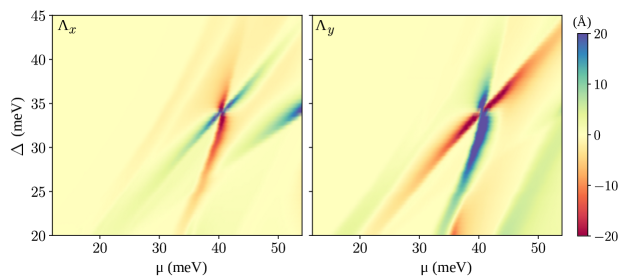
To emphasize the topological phase-transition more comprehensively we have plotted the - and -components of BCD as a function of perpendicular electric field () and chemical potential () in Supplementary Fig. S4 in presence of 0.1 strain along zigzag direction (). A clear sign of perpendicular electric field induced phase-transition can be realized from the butterfly like structure near meV. Before the phase-transition ( meV) the -component of BCD of the first conduction band has positive sign (shown by the blue lobe) and the second conduction band has negative sign (shown by the red lobe). However, after the phase-transition this trend gets reversed as the first conduction band possesses negative BCDx (shown by the red lobe) and the second conduction band possesses positive (shown by the blue lobe). Apart from the fact that the sign of the -components of the BCD is opposite to the corresponding -component, also shows a similar behavior. This abrupt change in the sign of BCD near 34 meV indicates a topological transition. We emphasize here that we have considered to reside in the maxima of the valence band and the shaded region near 50 meV is contribution of the further higher conduction bands to the BCD.
V Origin of BCD in graphene based moiré materials
In this section we explore the origin of large BCD in graphene based moiré systems, in vicinity of the charge neutrality point. For that we calculate Berry curvature dipole for a low energy tilted massive Dirac model and extend it to strained two band model of twisted bilayer graphene [40]. The nonlinear Hall conductivity for a tilted massive Dirac Hamiltonian of the form
| (S7) |
can be written as in the limit , which is valid for transport experiments. Up to linear order in the tilt value, the -component of the BCD at chemical potential is given by
| (S8) |
From this expression we infer that within the constant scattering time approximation the BCD is proportional to the tilt and the BCD peak in -axis is determined by the tilt and Berry curvature hotspot.
The low energy mode for strained twisted bilayer graphene given, in vicinity of the charge neutrality point, is given by [40]
| (S9) |
Here, with and the various velocities are modified by strain as shown in Ref. [40]. In Eq. (S9) while are determined by the off-diagonal components of strain matrix, the other components are determined by the diagonal components of strain matrix [40]. For a rough estimation, we will consider shear strain (diagonal components of strain are zero) where the tilt velocity is given by
| (S10) |
Using this tilt value in Eq. (S8), we have
| (S11) |
This simple estimate indicates that the BCD is larger for systems with i) large moiré lengthscale, and ii) with a large strain.
VI Scaling of nonlinear Hall Effect
In this section we describe the scaling law of the experimentally measured quantity which is related to the theoretically calculated nonlinear Hall conductivity and Drude conductivity as
| (S12) |
The non-linear Hall conductivity can originate from three different sources: i) the Berry curvature dipole, ii) side-jump scattering and iii) skew-scattering (also called anti-symmetric scattering). For a tilted massive Dirac model Hamiltonian it can be shown that [39] the Berry curvature dipole and the side-jump contributions to are inversely proportional to the impurity concentration making the ratio in Eq. (S12) to be scattering independent. However, the skew-scattering part has different impurity concentration dependence. Accounting for all the terms, we can write a general scaling relation, following Du et al. [39],
| (S13) |
Here, represent different source of scattering, the superscripts in, sj and sk stands for Berry curvature dipole, side-jump and skew-scattering contributions respectively. Considering only two sources of scattering, the static (impurities) and dynamic (phonon), we can write the above equation as follows
| (S14) |
Here, is the residual resistivity and is the dynamical resistivity. The new parameter set in Eq. (S14) can be obtained from the old one as
| (S15) | |||||
| (S16) | |||||
| (S17) |
For finite temperature, using , we can write the scaling law in terms of the conductivities as
| (S18) |
For experimental fitting we use a more simplified scaling law which reads as
| (S19) |
where represents the slope and is the intercept. From Eq. (S18) it is evident that the slope does not include any Berry curvature dipole contribution and is solely determined by the skew-scattering and side-jump mechanism. The intercept contains information of BCD.
VII NLH voltage from other TDBG devices
In Supplementary Fig. S5a and Supplementary Fig. S5b, we show the dependence of longitudinal resistance and nonlinear Hall voltage, respectively, on filling factor and displacement field . The data is taken from device-1 presented in main manuscript having a twist angle of 1.1∘, using a different set of probes. Supplementary Fig. S5c and Supplementary Fig. S5d shows the dependence of longitudinal resistance and nonlinear Hall voltage, respectively, on and from a different TDBG device (device-2) with a twist angle of 1.26∘. The additional vertical feature of high resistance in Supplementary Fig. S5c close to cm-2 can be attributed to moiré gap from a regime in device-2 having a slightly different twist angle of 1.09∘. Twist angle angle variation in same device is a signature of strain that breaks symmetry and give rise to BCD. In all the cases, the characteristic cross and halo feature that is present in the longitudinal resistance color plots (in Supplementary Fig. S5a, Supplementary Fig. S5c herein and also in Fig. 2a of main manuscript) is absent in the NLH voltage color plots (in Supplementary Fig. S5b, Supplementary Fig S5d herein and also in Fig. 2b of main manuscript). This shows the universality of NLH voltage across multiple TDBG devices and that the NLH signal only persists close to either the CNP or the moiré gaps, as discussed in the main manuscript.
VIII Characterization of NLH voltage
VIII.1 Quadratic nature
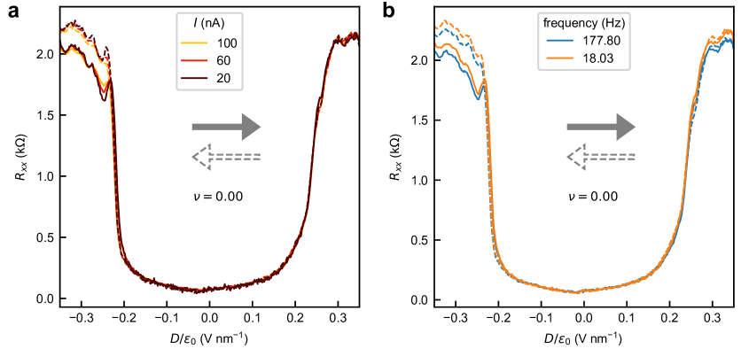
In Supplementary Fig. S6a, we show the quadratic scaling of the NLH voltage () with current for the same filling used in Fig. 3a and 3b of main manuscript. In Fig. S6b shows the linear dependence of on square of the longitudinal voltage (). A linear behavior establishes quadratic scaling of NLH voltage, that we measure, with current. Supplementary Fig. S6a and Supplementary Fig. S6b together shows that the quadratic nature persists in the regime of displacement field we use to extract BCD in Fig 3b of main manuscript. Supplementary Fig. S6c shows the quadratic scaling of the NLH voltage that corresponds to a filling close to the electron-side moiré gap. We see departure from linear behavior in Supplementary Fig. S6d for few displacement fields towards high values of 2. This is outside the scope of our present study.
VIII.2 Phase
In Supplementary Fig. S7, we show the phase of the measured NLH voltage as a function of displacement field for the filling . The filling and the range of displacement field is same to that we explore in Fig. 3a and 3b of main manuscript. When an ac current is sent, quadractic scaling of the second harmonic NLH voltage dictates that . The phase remains close to 90∘ across the two regimes, which is consistent to the second order nature of . We additionally note that we measured the out-of-phase component of the NLH voltage consistently throughout all the data presented in main manuscript and supplementary.
VIII.3 NLH voltage at other frequency
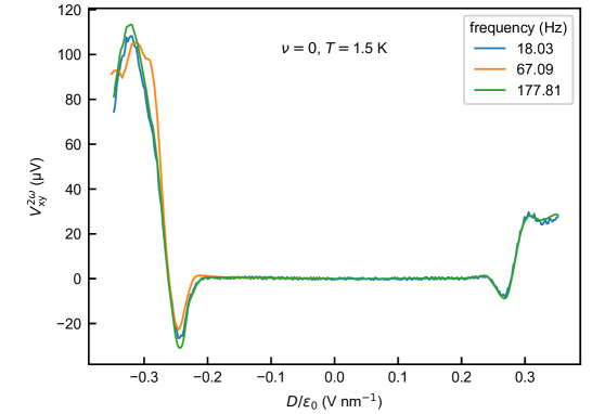
Supplementary Fig. S8 shows the nonlinear Hall voltage () dependence on displacement field for three different frequencies of the driving current. No frequency dependence of is observed even when the frequency we explored is varied by an order of magnitude (from 18-178 Hz). This is consistent to earlier reports [17, 18, 23]. Theoretically, independence of NLH voltage with frequency in the low-frequency regime such that , where is the frequency and is the scattering time, is a signature that the NLH voltage is BCD-induced [11].
IX Scaling of NLH voltage with conductivity
IX.1 /()2 vs using displacement field as parameter for different fixed temperature
In Supplementary Fig. S9a, we show the dependence of /()2 on () using as a parameter for the same filling where the range of extends below 0.175 V/nm (in Fig. 3b of main manuscript, is varied till 0.175 V/nm). We see that at lower displacement fields, /()2 is close to zero. Interestingly, from Extended Data Fig. 3b, we note that as the magnitude of displacement field is decreased to below 0.18 V/nm, the vs at becomes metallic, indicating a closing of the gap between the flat bands. Supplementary Fig. S9b shows /()2 dependence on at an elevated temperature of K for the same filling . Here, we see that the intercept is very close to zero in regime-I as well, that was otherwise nonzero at K in Supplementary Fig. S9a. The inset in Supplementary Fig. S9b shows the variation of the y-intercept in regime-I, as a function of temperature. Systematic variation of the intercept (or, /()2 for ) with confirms additionally that /()2 for , as we extract in Fig. 3d of main manuscript, is related to BCD.
IX.2 Extracting BCD via a second method
For low frequency, the BCD () can also be represented as [18, 11]
| (S20) |
Here, is the longitudinal conductivity, is the nonlinear Hall voltage, W is the width of TDBG, is the scattering time, is the current sent with low frequency and is the electronic charge. Using Drude formula, , where is the charge density and m is the effective mass, and (for our case, length ()=width ()=2 ) in eq. (S20), we obtain
| (S21) |
In Supplementary Fig. S10, we plot the BCD using eq. (S21) using for (the y-intercept in Fig. 3b of main manuscript) for different fillings . Here, cm-2 is the required charge density to completely fill the flat conduction band, corresponding to a twist angle of 1.1∘. With an assumption of m=3, where is mass of electron, we get a good agreement with the BCD extracted in Fig. 3c of main manuscript.
X Additional hysteresis data
X.1 Repeatability and histogram
X.2 Temperature dependence

X.3 Effect of current and frequency
X.4 Data for other fixed
X.5 Rate dependence
X.6 hysteresis data from another device

XI Polarization calculation details
XI.1 Computational Details
Our first-principles calculations are based on density functional theory (DFT) as implemented in Quantum ESPRESSO (QE) package [6]. We use ultrasoft pseudopotentials to represent the interaction between ionic cores and valence electrons. The exchange-correlation energy of electrons is treated within a generalized gradient approximation (GGA) [7] with a functional form parameterized by Perdew, Burke, and Ernzerhof [8]. We truncated the plane wave basis used in expansion of Kohn-Sham wave functions and charge density with energy cut-offs of 45 Ry and 360 Ry respectively. We used uniform grid of k-points for sampling the Brillouin zone (BZ) integrations. The discontinuity in occupation numbers of electronic states was smeared with broadening temperature of kBT = 0.005 Ry using a Fermi-Dirac distribution function. We include van der Waals (vdW) interaction using PBE + D2 method of Grimme [9]. The 2D system is simulated using a periodic supercell, with a vacuum layer of 12 Å separating adjacent periodic images of the sheet. To simulate response to electric field, we add a saw-tooth potential as a function z.
XI.2 Results and Discussion
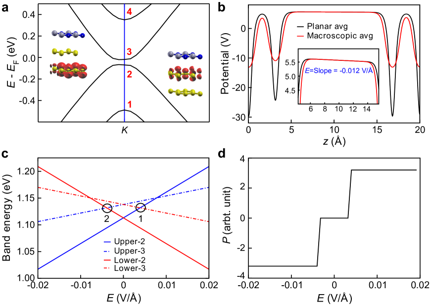
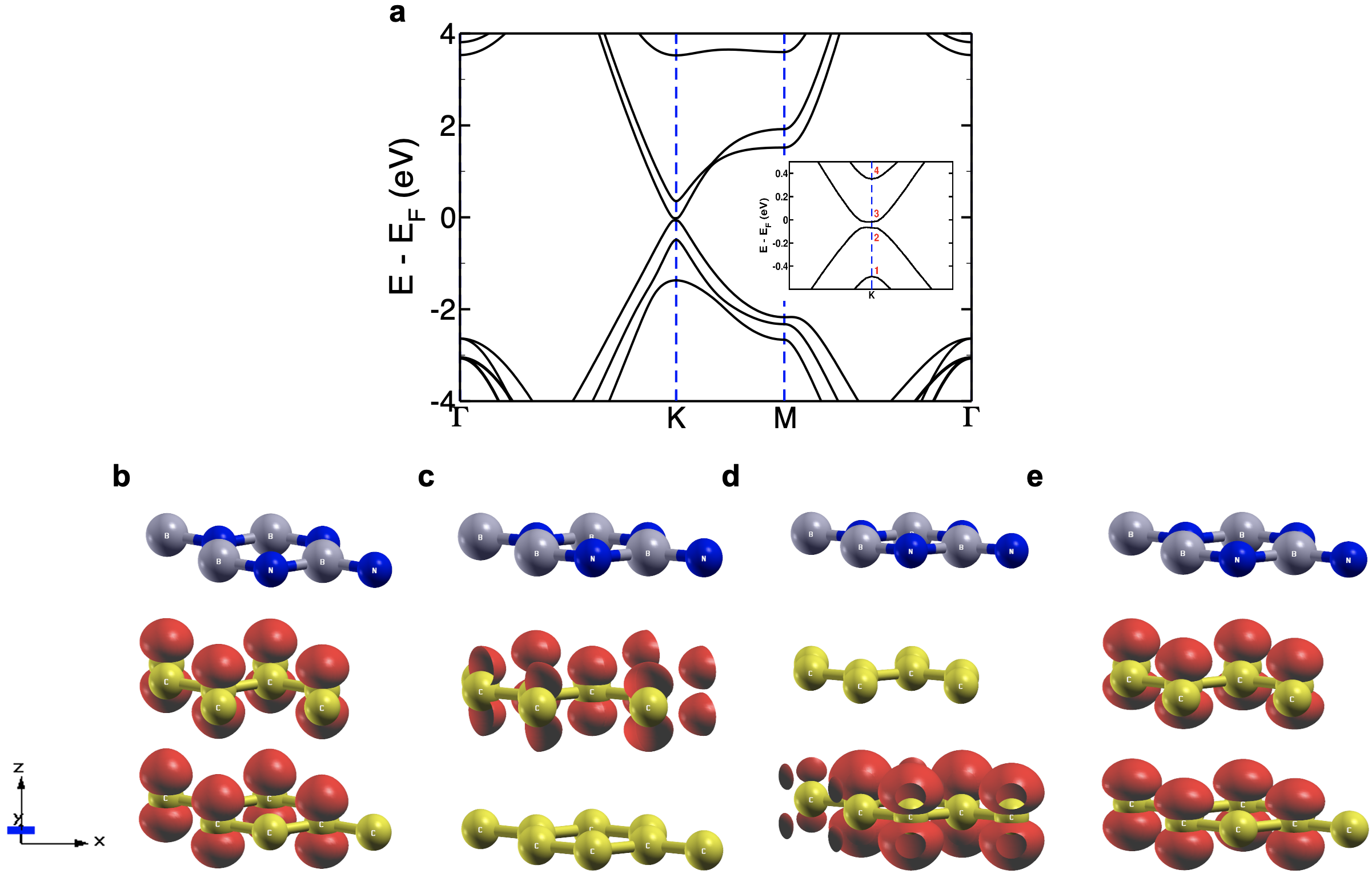
Twisted double bilayer graphene, TDBG, in our experiments is composed of two AB-stacked bilayers of graphene rotated by an angle [10] and encapsulated from top and bottom by hexagonal boron nitride (h-BN-TDBG-h-BN) (Supplementary Fig. S17b). Thus, parallelly stacked one atomic plane of hexagonal boron nitride and two layers of graphene (Gr-Gr-h-BN) is a building block making a half of h-BN-TDBG-h-BN (upper trilayer) (Supplementary Fig. S17a). Interestingly, a single Gr-Gr-h-BN unit is noncentrosymmetric and lacks the horizontal mirror symmetry. Hence, it is expected to have a non-vanishing polarization (dipole moment perpendicular to the plane). We consider two different configurations of Gr-Gr-h-BN which have been obtained by changing stacking sequences of Gr-Gr-h-BN (i) stacking of h-BN same as bottom graphene and (ii) stacking sequence of h-BN not matching with either of the two graphene layers. However, the energies of the two configurations are comparable (0.1 meV) and we carry out our theoretical analysis with the first configuration as a model.
We first examine the electronic structure of Gr-Gr-h-BN and find a band gap of 26 meV at K point (h-BN breaks sublattice symmetry of AB-stacked bilayer graphene, Supplementary Fig. S18a). From the slope of macroscopic average electrostatic potential in vacuum, our estimate of polarization of Gr-Gr-h-BN is Pz -0.34 C/cm2 (Extended Data Fig. 5b). Thus, Gr-Gr-h-BN has a nonzero polarization due to the broken inversion and horizontal reflection symmetries. This mechanism is similar to ferroelectricity in bilayer h-BN [4]. The lower trilayer of TDBG is h-BN-Gr-Gr (Supplementary Fig. S17c) and has exactly the same polarization with opposite sign.
The sense of hysteresis in longitudinal and nonlinear Hall voltage for doping just below charge neutrality point (CNP) is flipped on changing the doping to a point just above CNP. To understand the metastable states governing this hysteresis, we present a rigid band model for h-BN-Gr-Gr (lower trilayer) and Gr-Gr-h-BN (upper trilayer) of electronic states coupling with electric field and determine polarization as a function of electric field. Evolution of band energies with perpendicular electric field is modeled as
| (S22) |
where i is the band index (i = 1 to 4 for the four bands close to Fermi at K point), i is energy of ith band, e is charge of an electron, E is electric field, is the average position of each state (Supplementary Fig. S18b-e). is minus (-) for h-BN-Gr-Gr (lower trilayer) and plus (+) for Gr-Gr-h-BN (upper trilayer), respectively. Band 2 of the lower trilayer and band 3 of upper trilayer cross at E = -0.0039 V/Å (band 3 of lower trilayer and band 2 of upper trilayer cross at E = 0.0039 V/Å), resulting in redistribution of charges among these bands (Extended Data Fig. 5c). We show that there exist two metastable states for (i) E -0.0039 V/Å and (ii) E 0.0039 V/Å, with distinct polarization states in h-BN-TDBG-h-BN, that can be accessed with electric field within our rigid band model (Extended Data Fig. 5d). However, the resistance associated with the two metastable states remains the same. While the metastable states in h-BN-TDBG-h-BN are explained using the rigid band model, the hysteresis in resistance seen in experiments can originate from the broken symmetry, which can possibly arise from the distinction in coupling of top and bottom gates inducing inhomogeneous doping in the channel or by a twist between two trilayers.
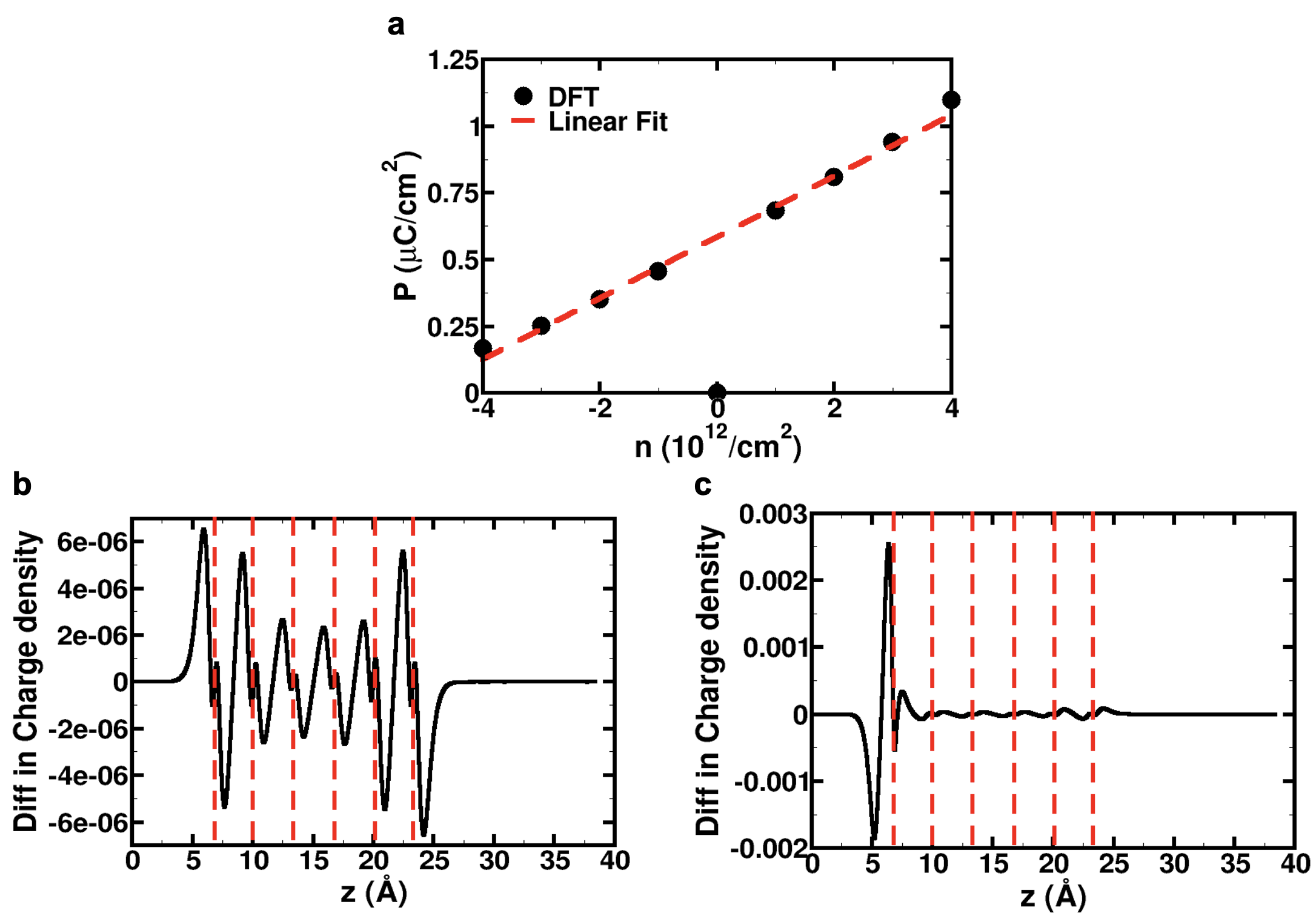
To understand the role of a gate electrode, we obtain the difference in planar-averaged electron charge density, (z) for n = 4 1012/cm2, E = 0.00625 V/Å and n = 4 1012/cm2, E = 0 V/Å with and without electric boundary conditions of a gate (Supplementary Fig. S19b and S19c) in h-BN-TDBG-h-BN with a twist angle = 21.78o. Asymmetry in at the atomic planes (red dashed lines in Supplementary Fig. S19b and S19c) indicate accumulation and depletion of electronic charge and local polarization arising from polarizability of pz orbitals and a transfer of a tiny amount of charge. In the presence of gate, a positive electric field (along ) pushes the electrons to the bottom gate (the scale of y-axis in Supplementary Fig. S19c is higher than Supplementary Fig. S19b), highlighting the inhomogeneity in doping. We note that a spontaneous electric dipole pz can also arise from the restructuring of the regions with AA, AB, BA and BB stacking upon application of electric field [4] and contribute to the observed hysteresis.
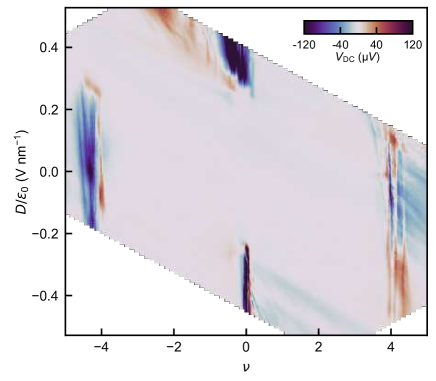
XII DC voltage
Apart from the second harmonic voltage , the nonlinear Hall effect also gives rise to a DC voltage [11, 17]. In Supplementary Fig. S20, we show the measured DC voltage in perpendicular direction to an ac current applied with frequency 177 Hz. The dependence of the DC voltage is shown for the full parameter space of (,) for the same device used to show the NLH voltage dependence in Fig. 2b of main manuscript. DC voltage, together with the measured second harmonic , provides additional evidence for NLH effect in TDBG devices.
References
- [1] Bistritzer, R. & MacDonald, A. H. Moiré bands in twisted double-layer graphene. Proceedings of the National Academy of Sciences 108, 12233–12237 (2011).
- [2] Bi, Z., Yuan, N. F. Q. & Fu, L. Designing flat bands by strain. Physical Review B 100, 035448 (2019).
- [3] Wang, Y.-X., Li, F. & Zhang, Z.-Y. Phase diagram and orbital chern insulator in twisted double bilayer graphene. Physical Review B 103, 115201 (2021).
- [4] Koshino, M. Band structure and topological properties of twisted double bilayer graphene. Physical Review B 99, 235406 (2019).
- [5] Mohan, P., Ghorai, U. & Sensarma, R. Trigonal warping, satellite dirac points, and multiple field tuned topological transitions in twisted double bilayer graphene. Physical Review B 103, 155149 (2021).
- [6] Giannozzi, P. et al. Quantum espresso: a modular and open-source software project for quantum simulations of materials. Journal of physics: Condensed matter 21, 395502 (2009).
- [7] Hua, X., Chen, X. & Goddard, W. Generalized generalized gradient approximation: An improved density-functional theory for accurate orbital eigenvalues. Physical Review B 55, 16103 (1997).
- [8] Perdew, J., Burke, K. & Ernzerhof, M. Perdew, Burke, and Ernzerhof reply. Physical Review Letters 80, 891 (1998).
- [9] Grimme, S. Accurate description of van der Waals complexes by density functional theory including empirical corrections. Journal of computational chemistry 25, 1463–1473 (2004).
- [10] Cocemasov, A. I., Nika, D. L. & Balandin, A. A. Phonons in twisted bilayer graphene. Physical Review B 88, 035428 (2013).